المنتجات (19,000+)

T4160NSN7TTB - QorIQ 16-Core 1.8GHz Power Arch MPU | NXP
T4160NSN7TTB

T4160NSN7TTB - QorIQ 16-Core 1.8GHz Power Arch MPU | NXP

The NXP (formerly Freescale) T4160NSN7TTB is a QorIQ T4-series communications microprocessor built on a 64-bit Power Architecture e6500 core complex, delivering 16 hardware threads across 8 dual-threaded cores at up to 1.8 GHz, in a 1932-ball FC-PBGA package (45x45 mm). It is the 16-thread member of the T4 family, pin-compatible with the 24-thread T4240 and 8-thread T4080 within a 3x performance scaling envelope. What is a QorIQ communications processor? A QorIQ processor is a multi-core Power Architecture microprocessor designed by NXP for networking and data-plane workloads such as routers, switches, wireless baseband, and security appliances. As a category, QorIQ sits in the hierarchy: microprocessor unit (MPU) -> embedded processor -> communications processor -> networking SoC. The T4 family targets high-end control-plane and data-plane processing for terabit-class routers, service-provider gateways, and network-attached storage. Key features of the T4160NSN7TTB include a 1.8 GT/s DDR3L memory controller with ECC, integrated 4x 10 Gigabit Ethernet (10GE) plus 8x 1 Gigabit Ethernet (1GE) SerDes lanes, hardware cryptography disabled in this -NS suffix (T4160NS variant), and operating junction temperature support of 0C to 105C in Rev 2.0 silicon. The device integrates packet-processing acceleration engines, a high-bandwidth CoreNet coherency fabric, and extensive I/O including PCIe, SATA, and USB. Architecturally, the e6500 cores support hardware multithreading (SMT), out-of-order execution, and AltiVec SIMD, with a triple-issue superscalar pipeline. The CoreNet coherency fabric ensures coherency across cores and accelerators at high throughput, while the memory subsystem delivers 1.8 GT/s aggregate bandwidth to feed 16 threads without contention. Crypto variants (T4160NSN7TTB's crypto-disabled sibling T4160NSE) integrate SEC engines for IPsec and SSL offload. Typical applications include enterprise routers, service-provider edge platforms, network security appliances, LTE/WCDMA baseband processing, and high-end network-attached storage (NAS) controllers. The 16-thread configuration balanced against 10GE+1GE SerDes makes it well-suited to mid-range multi-service aggregation platforms. When designing with the T4160NSN7TTB, ensure the PCB land pattern uses the 45x45 mm FC-PBGA with a 16-layer or higher stack-up to manage the 1.8 GT/s DDR3L signals with matched impedance. Reference the NXP hardware design checklist for decoupling, SerDes routing, and thermal management. This page synthesizes distributor pricing, drop-in NXP T4-family alternatives, and design considerations not found in the manufacturer datasheet alone.

طلب عرض سعر اتصل بنا
T4160NXN7PQB - QorIQ 16-Core 1.5GHz SoC | NXP Semiconductors
T4160NXN7PQB

T4160NXN7PQB - QorIQ 16-Core 1.5GHz SoC | NXP Semiconductors

The NXP T4160NXN7PQB is a 64-bit Power Architecture QorIQ T4 family multicore communications processor with 16 virtual cores running at 1.5 GHz, housed in a 1932-pin FCPBGA (45x45 mm) package. It integrates a dual-channel DDR3L memory controller with up to 1.6 GT/s data rate, dual 10 Gigabit Ethernet MACs, and SerDes for high-speed I/O, with hardware cryptography disabled in this revision (Rev 2.0). Industrial temperature grade is -40C to +105C. A multicore communications SoC (System-on-Chip) is a single silicon die that integrates CPU cores, memory controllers, networking accelerators, and I/O subsystems onto one chip. The QorIQ family is built on the 64-bit Power Architecture (formerly PowerPC) instruction set, scaled for embedded networking and industrial workloads. The T4 family spans T4080 (8 threads), T4160 (16 threads), and T4240 (24 threads) in a pin-compatible package, giving designers a 3x performance scaling path on one PCB. Key features include 16 threads (8 dual-threaded e6500 cores) at 1.5 GHz, 1.6 GT/s DDR3L with ECC, two 10 Gigabit Ethernet interfaces, hardware cryptography disabled, and extended temperature operation to +105C. The 28nm process gives improved performance-per-watt versus earlier QorIQ generations, while preserving software compatibility across the T4 series. The T4160NXN7PQB ships as a tray-packaged part intended for high-density networking and industrial computing platforms. The architecture combines out-of-order Power Architecture cores with a coherent CoreNet fabric, enabling efficient parallel packet processing. The SerDes block supports multiple protocols including XAUI, XFI, KR, and SGMII, allowing direct connection to 10G/1G PHYs without external glue logic. Hardware accelerators offload pattern matching, CRC, and queue management, dramatically reducing CPU load in deep-packet-inspection workloads. The integrated security engine is present but disabled in this part revision - derivative SKUs with crypto enabled exist for adjacent use cases. Typical applications include enterprise routers and switches, network appliances, industrial control gateways, telecom base-station controllers, and aerospace/defense packet processors. The 16-thread configuration is well-suited to mid-range networking workloads - heavy enough for line-rate 10G processing yet within the power envelope of passively-cooled industrial chassis. When designing with this device, allocate a multi-layer PCB with at least 8 layers for signal integrity across the high-speed SerDes and DDR3L interfaces. The 1932-ball FCBGA requires a substrate with microvia stack-ups and matched-length routing. Thermal management must consider the 1.5 GHz core clock under sustained load - a heatsink and airflow path are required at industrial temperatures above +85C. This page synthesizes distributor pricing from Mouser and DigiKey Marketplace, NXP family-level alternative guidance, and practical layout guidance for the FCBGA-1932 footprint - information that complements the official QorIQ T4 datasheet without replacing it.

طلب عرض سعر اتصل بنا
T4240NSE7PQB - 24-Core QorIQ Power Arch SoC | NXP
T4240NSE7PQB

T4240NSE7PQB - 24-Core QorIQ Power Arch SoC | NXP

The NXP T4240NSE7PQB is the flagship QorIQ T4 series communications processor with 24 virtual cores based on the 64-bit Power Architecture e6500 core, running up to 1.5 GHz (1.8 GHz capable), in a 1932-ball FCPBGA package (45x45 mm). It integrates 1.6 GT/s DDR3L memory controllers and four 10 Gigabit Ethernet (10GE) MACs with classified security/crypto acceleration enabled, operating across the 0 to +105C industrial junction temperature range, with silicon revision 2.0. The device is built in a 45 nm SOI CMOS process and targets line-rate packet processing across enterprise, service-provider, and data-center networking infrastructure. A QorIQ multiprocessor is a multi-core system-on-chip (SoC) tailored for data-plane workloads such as routing, switching, security, and protocol termination. Within the broader taxonomy, QorIQ belongs to the communications processor (CP) family, which sits hierarchically below general-purpose microprocessors and above single-core MCUs. Its core advantages are deterministic throughput on parallel threads (24 hardware threads via the e6500 dual-threaded core), tight integration of packet I/O, memory controller, and acceleration engines, and an extended lifecycle suited to embedded networking OEMs. Key features include 24 virtual cores delivered by 12 physical e6500 dual-threaded cores, an integrated memory subsystem supporting DDR3L at up to 1.6 GT/s with ECC, an integrated security engine (SEC) at up to 10 Gbps for IPsec, SSL/TLS, and SRTP, four 10G plus multiple 1G Ethernet controllers with hardware L2 switching and classification, and an Enhanced Triple Speed Ethernet (eTSEC) peripheral complement. The device also offers four PCIe Gen2 controllers, RapidIO, and a complete set of peripheral I/O for system integration. The T4240 implements a coherent shared-memory architecture with the CoreNet coherency fabric, allowing all 12 dual-threaded cores to share L2 caches and the integrated 1 MB L2 per cluster. The platform's 64-bit Power Architecture ISA, hardware hypervisor extensions, and dedicated resource partitioning make it suitable for multi-tenant virtualized networking appliances. Typical applications include top-of-rack and spine switches, enterprise routers with 10G/40G uplinks, network security appliances (firewalls, UTM, IPS/IDS), wireless infrastructure controllers, and data-center server/load balancers. Its 24-thread envelope is particularly well suited to software-defined networking (SDN) control plane plus line-rate classification workloads. When designing with this device, allocate ample PCB real estate for the 1932-ball FCPBGA, follow NXP's reference design for power sequencing and SerDes reference clock jitter, and provision at least 8-layer PCB with controlled-impedance routing for the 10G KR lanes to meet IEEE 802.3ap compliance. This page synthesizes distributor pricing, drop-in same-package alternatives from the T4 family, and practical design considerations beyond the manufacturer datasheet summary.

طلب عرض سعر اتصل بنا
T4240NSN7TTB - QorIQ T4 24x 1.8GHz Power Arch MPU | NXP
T4240NSN7TTB

T4240NSN7TTB - QorIQ T4 24x 1.8GHz Power Arch MPU | NXP

The NXP T4240NSN7TTB is the flagship QorIQ T4 communications processor, integrating 12 PowerPC e6500 cores running up to 1.8 GHz (24 threads with hardware multithreading), a 1.8 GT/s DDR3L memory controller, and 4x 10 Gigabit Ethernet ports in a 1932-ball FCBGA (45x45 mm) package. Crypto acceleration is disabled in this -N suffix variant, and the device is qualified for 0 to 105 degrees C operation on silicon revision 2.0. A QorIQ communications processor is a member of the multicore Power Architecture microprocessor family specifically engineered for networking and embedded infrastructure workloads. Within the broader system hierarchy, QorIQ T series sits below: QorIQ T family -> QorIQ communications processor -> Power Architecture microprocessor -> embedded MPU -> integrated circuit. These parts are positioned for routers, switches, base stations, and other data-plane equipment where deterministic throughput and high SerDes lane counts are critical. Key features include 12 dual-threaded e6500 cores providing 24 threads, 64 KB I-cache and 32 KB D-cache per core plus a shared 2 MB L2 per cluster, a 64-bit DDR3L interface supporting 1.8 GT/s with ECC, integrated 10 Gbps SerDes, multiple PCI Express Gen 2 controllers, and the Data Path Acceleration Architecture (DPAA) for hardware offload of classification, queueing, and crypto. The 45x45 mm FCBGA package exposes 1932 balls and supports high-speed signal escape required for the multi-lane SerDes. The T4240 is fabricated in 28 nm CMOS process technology and pairs the e6500 cores with NXP's CoreNet coherency fabric. The four 10 Gbps ports can also be configured as multiple 1 GbE lanes, giving designers flexibility to scale from 1G to 40G aggregate Ethernet. The architecture enables line-rate processing for routing, deep-packet inspection, and traffic management without external lookup engines. Typical applications include enterprise routers, edge gateways, network attached storage controllers, LTE and 5G base station baseband, industrial control planes, and military secure communications platforms. The wide SerDes integration makes the T4240 particularly attractive where PCB real estate and power efficiency both matter. When designing with the T4240, allocate a minimum of a 12-layer PCB stack-up to route the DDR3L byte lanes and 10G SerDes with controlled impedance. Decoupling requires roughly 50 low-ESR ceramic capacitors distributed near the core and SerDes rails, and thermal design must assume up to 35 W TDP under full thread load. This page synthesizes distributor pricing, drop-in alternatives within the T4 family, and practical design notes not found in the manufacturer datasheet.

طلب عرض سعر اتصل بنا
TC222L16F133NACKXUMA1 - AURIX 32-Bit MCU 133MHz 1MB Flash | Infineon
TC222L16F133NACKXUMA1

TC222L16F133NACKXUMA1 - AURIX 32-Bit MCU 133MHz 1MB Flash | Infineon

The Infineon TC222L16F133NACKXUMA1 is an AURIX TC2xx family 32-bit TriCore microcontroller IC running at 133 MHz with 1 MB on-chip Flash program memory and 96 KB SRAM (including cache), housed in an 80-lead PG-TQFP-80-7 (HTFQFP, exposed pad) package with gull-wing leads and automotive-grade temperature rating. The TC22xL sub-family is positioned as the entry point of the AURIX TC2xx generation for safety-critical chassis, body, and powertrain applications where deterministic computation and integrated peripherals reduce system cost. A microcontroller (MCU) is a single-chip computer that integrates a CPU core, volatile and non-volatile memory, peripherals, and interrupt control on one die. AURIX TriCore combines a RISC-like microcontroller core, a DSP arithmetic unit, and a super-scalar pipeline in one ISA, allowing efficient mixed control-and-signal-processing workloads. The TC22xL belongs to the AURIX microcontroller family, which itself sits within Infineon's embedded processing portfolio and the broader 32-bit automotive MCU category alongside Traveo and PSoC families. Key features of the TC222L16F133NACKXUMA1 include 3 CAN nodes, 133 MHz maximum TriCore clock, 1 MB Flash with 96 KB SRAM, and a 12-bit A/D converter with up to 16 input channels for analog sensing. The device also integrates timers, ASCLIN SPI/UART, and hardware security modules (HSM) for secure boot and cryptographic acceleration. Automotive-grade qualification and a -40C to +125C (or higher) junction-temperature range make it suitable for under-hood and chassis ECUs. Peripheral integration reduces external component BOM compared with discrete MCU plus external ADC designs. Typical applications for TC222L16F133NACKXUMA1 cover electric power steering (EPS), electronic stability control (ESC), airbag systems, body control modules (BCM), and transmission control units (TCU). It is also used in sensor fusion ECUs and zone controllers in zonal vehicle E/E architectures. The integrated HSM and lockstep-capable timers make it a popular choice for ASIL-B/D rated subsystems in next-generation vehicle designs. When designing with this part, ensure PCB layout follows the exposed-pad thermal recommendations - the die is thermally coupled to the package bottom pad and must be soldered to a sufficiently large copper area. The 80-pin TQFP-80 (HTFQFP) footprint requires a 0.5 mm pitch land pattern; reflow profile must respect the moisture-sensitivity level printed on the reel label. Always refer to the Infineon AURIX TC22xL datasheet family for full register definitions and HSM provisioning steps. This page synthesizes distributor pricing tiers, drop-in AURIX family alternatives, and practical automotive-ECU design notes not collected in any single manufacturer datasheet revision.

طلب عرض سعر اتصل بنا
TC222S16F133FACKXUMA1 - AURIX TC22xL 32-Bit MCU 1MB Flash | Infineon
TC222S16F133FACKXUMA1

TC222S16F133FACKXUMA1 - AURIX TC22xL 32-Bit MCU 1MB Flash | Infineon

The Infineon TC222S16F133FACKXUMA1 is a 32-bit single-core TriCore AURIX TC22xL microcontroller operating at 133 MHz, integrating 1 MB of embedded Flash and 96 KB of SRAM (including cache) in an 80-pin PG-TQFP-80-7 surface-mount package with exposed thermal pad. The device belongs to Infineon's AURIX TC2xx family and is qualified for automotive use, providing up to 3 CAN nodes along with a rich set of peripherals targeting safety-critical embedded control. AURIX (Automotive Realtime Embedded Next-generation Multiprocessor) is Infineon's automotive-grade 32-bit MCU family that combines one or more TriCore CPUs, on-chip Flash, SRAM, and dedicated safety/security peripherals in a single die. Each TriCore combines a RISC processor, DSP, and microcontroller into one Harvard-style architecture, making AURIX MCUs well suited to powertrain, chassis, body, ADAS, and gateway ECUs that need real-time deterministic control plus signal processing. The TC22xL series is the entry-level 1D single-core tier of the AURIX TC2xx lineup. Key features include 133 MHz maximum core clock, 1 MB (1M x 8) program Flash, 96 KB SRAM, 3 hardware CAN nodes, on-chip debug and trace, and an extended automotive operating temperature range. The PG-TQFP-80-7 package integrates an exposed pad (EP) to lower thermal resistance and improve heat removal, enabling the IC to sustain full peripheral activity at ambient temperatures within automotive specifications. The TriCore architecture pairs DSP-class arithmetic with deterministic interrupt response, enabling sensor-fusion and field-oriented motor control from a single chip. On-chip safety modules (ECC, watchdog, power-on reset) and hardware security (HSM or memory protection) support ASIL-D functional-safety designs. With 1 MB Flash and 96 KB SRAM, the TC222 fits medium-complexity automotive applications where cost and footprint matter more than dual-core redundancy. Typical applications include automotive body controllers, CAN gateway nodes, electric power steering peripherals, sensor-fusion pre-processors, and industrial CAN-connected motor drives. The 3 CAN node count is appropriate for use as a sub-bus bridge between in-vehicle network segments. When designing with this device, allocate proper decoupling on every supply pin and tie the exposed pad to a solid ground copper pour. Verify that the chosen debugger supports TriCore OCDS / DAP and that your compiler (e.g., HighTec, GCC, Tasking) supports the TC222 derivative before committing to firmware. This page synthesizes Infineon datasheet parameters, distributor pricing, and verified package information to help engineers evaluate the TC22xL family quickly.

طلب عرض سعر اتصل بنا
TC265D40F200WBCKXUMA1 - AURIX 32-bit MCU, 2.5MB Flash, 200MHz, LQFP-176 | Infineon
TC265D40F200WBCKXUMA1

TC265D40F200WBCKXUMA1 - AURIX 32-bit MCU, 2.5MB Flash, 200MHz, LQFP-176 | Infineon

The Infineon TC265D40F200WBCKXUMA1 is an AURIX TC26xD family 32-bit dual-core TriCore microcontroller running at 200 MHz with 2.5 MB of embedded Flash and 176-pin LQFP-EP packaging, qualified to AEC-Q100 for automotive applications. The device integrates a high-performance TriCore v1.6 CPU subsystem with DSP and addressable SRAM, on-chip flash, and a peripheral set tailored to powertrain, chassis, and safety ECUs. A microcontroller (MCU) is a single-chip computer that integrates a CPU core, memory (Flash + SRAM), peripherals, and I/O on one silicon die. The AURIX TC2xx family is engineered for safety-critical embedded systems, combining lockstep TriCore cores, hardware security modules, and ASIL-D capable peripherals. Within the broader taxonomy, the TC265D40F200WBCKXUMA1 belongs to: MCU -> 32-bit MCU -> TriCore architecture -> AURIX family -> TC26xD sub-family -> automotive-grade MCU. Key features include 2.5 MB of program Flash, on-chip SRAM, a 200 MHz dual-core TriCore CPU with DSP instructions, and a rich peripheral mix including multiple CAN-FD nodes, SPI, LIN, QSPI, ASCLIN, and timers. The part also embeds a Programmable HSM (Hardware Security Module) for secure boot, key storage, and EVITA-Full cryptography, along with a GTM (Generic Timer Module) for complex PWM and motor-control tasks. The TC26xD implements Infineon's TriCore instruction set, which fuses RISC, DSP, and microcontroller paradigms in a single load/store architecture with deterministic interrupt latency. Built on a 40 nm embedded Flash process, it operates from a 3.3 V / 5 V supply with internal core logic on a separate voltage domain. Memory protection, ECC on Flash/SRAM, and lockstep compare logic support ASIL-D safety integrity when configured in dual-core lockstep mode. Typical applications include automotive body domain controllers, electric power steering, airbag ECUs, battery management systems, and industrial servo drives. The wide temperature range and integrated peripherals make it suitable for chassis, powertrain, and ADAS sensor fusion subsystems where deterministic performance and hardware security are mandatory. When designing with this part, provide at least four decoupling capacitors (100 nF + bulk) near each supply pin, follow Infineon PCB layout guidelines for the LQFP-176 EP package, and configure the HSM for secure boot before deploying production firmware. Use Infineon's AURIX Development Studio and the iLLD (Infineon Low-Level Driver) libraries to shorten firmware bring-up.

طلب عرض سعر اتصل بنا
TC275T64F200WDCKXUMA1 - 32-Bit TriCore AURIX MCU, 200MHz, 4MB Flash | Infineon
TC275T64F200WDCKXUMA1

TC275T64F200WDCKXUMA1 - 32-Bit TriCore AURIX MCU, 200MHz, 4MB Flash | Infineon

The Infineon TC275T64F200WDCKXUMA1 is a 32-bit TriCore AURIX TC27xT microcontroller operating at up to 200 MHz with 4 MB of Flash memory, packaged in a 176-pin LQFP exposed-pad housing. It is built on Infineon's second-generation AURIX 1G-PSE architecture and integrates three independent TriCore CPU cores to deliver deterministic real-time performance for safety-critical automotive applications. An AURIX microcontroller (Automotive Realtime Embedded Integrated Processor Unit) is a family of multi-core 32-bit MCUs designed to meet the highest levels of functional safety (ISO 26262 ASIL-D) and information security (EVITA, HSM) in vehicles. Within the broader hierarchy, AURIX sits at the intersection of automotive microcontroller, safety MCU, and powertrain control processor, serving as the silicon backbone for domain and zonal controllers. The TC27xT family specifically targets powertrain, chassis, and advanced driver-assistance systems (ADAS) requiring deterministic interrupt latency, lockstep cores, and hardware security modules. Key specifications include 200 MHz maximum clock frequency across three TriCore v1.6 cores, 4 MB (4M x 8) of embedded Flash, 472 KB SRAM inclusive of cache, four CAN nodes, multiple LIN and FlexRay interfaces, and a hardware security module. The 1.3 V/5 V supply domain supports both low-voltage logic and 5 V peripheral interfacing without external level shifters. The PG-LQFP-176-22 package includes an exposed thermal pad that lowers junction-to-ambient thermal resistance for high-temperature under-hood operation. The TC275T64F200WDCKXUMA1 leverages Infineon's lockstep architecture to support ISO 26262 functional safety up to ASIL-D, making it suitable for systems where faults must be detected within a single clock cycle. Compared to single-core MCUs, the three-core TriCore arrangement separates application processing, peripheral control, and safety monitoring tasks, eliminating the need for an external watchdog or companion safety MCU. According to the Infineon AURIX 1G-PSE datasheet, the device is qualified to AEC-Q100 Grade 0 for automotive environments. Typical applications include engine management ECUs, transmission control units (TCUs), chassis domain controllers, electric vehicle (EV) inverter control, braking and stability systems, and zonal vehicle compute platforms. The combination of CAN FD, FlexRay, and LIN connectivity makes it a strong fit for legacy and modern in-vehicle networking topologies. When designing with this part, allocate adequate PCB copper under the exposed pad to meet the theta_JA thermal budget; without a minimum 100 mm² copper pour the maximum operating temperature becomes derated. Program Flash in production via the integrated bootloader or via JTAG using an Infineon DAS device. Always validate the AURIX safety case against the latest Infineon application note package. This page synthesizes distributor pricing, pin-compatible drop-in alternatives, and practical design notes not found on the manufacturer datasheet, helping procurement and design engineers make informed sourcing decisions.

طلب عرض سعر اتصل بنا
TC297TP128F300SBCKXUMA1 - 300MHz TriCore AURIX 8MB MCU | Infineon
TC297TP128F300SBCKXUMA1

TC297TP128F300SBCKXUMA1 - 300MHz TriCore AURIX 8MB MCU | Infineon

The Infineon TC297TP128F300SBCKXUMA1 is a 32-bit TriCore automotive microcontroller from the AURIX TC29xT family, integrating three independent TriCore CPUs running at up to 300 MHz, 8 MB of embedded Flash and 728 KB of SRAM (including cache), in a PG-LFBGA-292-6 package. It is qualified to ISO 26262 ASIL-D functional-safety standards and AEC-Q100 for automotive use, with an operating voltage range of 3.3 V to 5 V and a junction temperature range of -40 °C to +125 °C. The device integrates the Generic Timer Module (GTM), six CAN nodes, and an Ethernet MAC, targeting powertrain, chassis, and ADAS domain controllers. Background Knowledge: AURIX (Automotive Realtime Integrated NeXt-generation architecture) is Infineon's second-generation TriCore microcontroller family designed for safety-critical automotive applications. TriCore combines the real-time capability of a microcontroller, the computational power of a DSP, and the interrupt responsiveness of a RISC CPU in a single core ISA. Within the AURIX taxonomy, TC29xT sits in the upper-performance tier: multicore (up to 3 TriCore CPUs), large Flash (8 MB), and abundant peripherals, supporting ISO 26262 ASIL-D system designs without external lockstep companion chips. Key features include three independent 300 MHz TriCore v1.6 CPUs, 8 MB program Flash with ECC, 728 KB SRAM, hardware security module (HSM) and EVITA-Full support, GTM for motor and timer orchestration, six CAN FD nodes, and 1 Gbit Ethernet. The 292-ball LFBGA package exposes the full peripheral set, including multiple SENT, PSI5, SPI, and LIN interfaces. Hardware over/under-voltage monitors and a built-in self-test (BIST) engine support ISO 26262 decomposition to ASIL-D at the system level. Architecturally, the TC297T uses lockstep and delayed-lockstep CPU pairs (depending on configuration) and dedicated checker cores to detect soft errors; the GTM provides parallel PWM and capture channels independent of CPU load, which is critical for deterministic motor control and fuel-injection timing. Memory is protected by ECC on Flash and parity/ECC on SRAM, and a Hardware Security Module isolates cryptographic keys for secure boot and OTA updates. Typical applications include automotive zone and domain controllers, electric-vehicle inverter and battery management controllers, ADAS sensor fusion pre-processors, chassis ECUs (braking, steering, suspension), and industrial safety controllers requiring IEC 61508 SIL-3. The combination of three cores and rich peripherals makes it well suited to chassis-domain ECUs where sensor acquisition, motor control, and vehicle-network gateway tasks run concurrently. When designing with this part, allocate generous PCB copper for the 292-ball LFBGA (a 4-layer minimum stack-up is recommended), keep analog 3.3 V supplies quiet (the EVRA regulator pin is noise-sensitive), and follow Infineon AURIX Application Note AP32267 for oscillator and PLL layout. The HSM must be provisioned before secure boot is enabled, so plan factory key injection in your manufacturing flow. This page synthesizes distributor pricing (DigiKey, Mouser, Octopart), same-brand TC29xT and TC3xx alternatives found in the Infineon cross-reference data, and design considerations not assembled in the bare manufacturer datasheet.

طلب عرض سعر اتصل بنا

TDA4VE88TGAALZRQ1 - 8 TOPS AI SoC | Texas Instruments
TDA4VE88TGAALZRQ1

TDA4VE88TGAALZRQ1 - 8 TOPS AI SoC | Texas Instruments

The Texas Instruments TDA4VE88TGAALZRQ1 is a high-performance automotive System-on-Chip (SoC) designed for vision perception and analytics. It integrates dual Arm Cortex-A72 processors running at 2 GHz, a Cortex-R5F real-time core at 1 GHz, C66x and C7x DSPs, and an 8 TOPS AI accelerator. The device also includes a GPU for graphics acceleration. It is offered in a 770-pin FCBGA (ALZ) package measuring 23x23 mm, supporting an operating temperature range of -40°C to +125°C. What is a System-on-Chip (SoC)? An SoC is a semiconductor device that integrates multiple computing units, including CPU cores, DSPs, GPU, AI accelerators, and memory interfaces, onto a single chip. It is a higher-level integration than a microprocessor, combining system functionality to reduce board complexity. In the automotive domain, SoCs are the central compute hub for ADAS, autonomous driving, and infotainment. Key features include dual 2 GHz Cortex-A72 cores for application processing, a 1 GHz Cortex-R5F for real-time control, and C66x and C7x DSPs for signal processing. The 8 TOPS AI accelerator enables deep learning inference at the edge, supporting tasks such as object detection and semantic segmentation. The integrated GPU provides 3D rendering capability for surround-view systems. The SoC uses a heterogeneous architecture to optimize power and performance. The A72 cores handle Linux-based automotive stacks, while the DSPs offload real-time sensor processing. The 770-pin FCBGA (ALZ) package offers excellent thermal performance with a 23x23 mm footprint, enabling dense system integration. The AEC-Q100 qualification ensures reliability across the automotive temperature range. Typical applications include ADAS domain controllers, autonomous driving systems, surround-view camera processing, radar signal processing, and in-vehicle infotainment. Its 8 TOPS AI is particularly suited for vision-perception systems where real-time object detection is critical. When designing with this SoC, ensure proper power sequencing using a PMIC like TPS6594-Q1 and adequate thermal management. The high-speed interfaces require careful PCB design with controlled impedance. Refer to TI's Jacinto 7 reference designs for guidance.

طلب عرض سعر اتصل بنا
TDA4VL21HGAALZRQ1 - 4 TOPS ADAS SoC | Texas Instruments
TDA4VL21HGAALZRQ1

TDA4VL21HGAALZRQ1 - 4 TOPS ADAS SoC | Texas Instruments

The Texas Instruments TDA4VL21HGAALZRQ1 is an automotive system-on-chip (SoC) from the Jacinto TDA4VL-Q1 processor family, engineered for vision perception and analytics. It integrates dual Arm Cortex-A72 cores running up to 2 GHz, Arm Cortex-R5F cores up to 1 GHz, C7x and C66x DSPs up to 1 GHz, an integrated GPU, and a deep-learning accelerator delivering 4 TOPS of AI performance. The device is housed in a 770-ball FCBGA (ALZ) package measuring 23 x 23 mm with 0.8 mm terminal pitch and is rated from -40C to +125C for automotive environments. An automotive vision SoC is a single-chip microprocessor (MPU) subsystem that combines a general-purpose application-processor cluster, a real-time MCU island, digital signal processors, dedicated neural-network acceleration, graphics, and rich automotive I/O on one die. Within the semiconductor hierarchy - semiconductor to microprocessor to system-on-chip to ADAS vision processor - the TDA4VL-Q1 represents the cost-optimized tier of TI's Jacinto platform, sharing its architecture, package technology, and software stack with the TDA4VE and TDA4AL family members under one datasheet. Key features begin with the 4 TOPS deep-learning engine, which executes object-detection, classification, and segmentation networks for camera-based ADAS. Heterogeneous compute lets the Cortex-A72 cluster run high-level operating systems while Cortex-R5F cores close real-time safety loops and the C7x/C66x DSPs accelerate vision kernels. Distributor parametric data lists a 0.84 V maximum core supply, 770 terminals, and device marking TDA4VL21 at silicon revision 1.0. Technically, the TDA4VL21HGAALZRQ1 is covered by the 251-page TI datasheet TDA4VE/TDA4AL/TDA4VL Jacinto Processors, Silicon Revision 1.0, confirming that the ball map, board design, and boot configuration are common across the three variants - a significant advantage for platform reuse and mid-cycle cost-downs. DigiKey and Mouser list the part as an automotive system-on-a-chip with AI accelerator in the 770-FCBGA (23x23) package. Typical applications include single front-camera ADAS ECUs using 4 TOPS neural inference, driver and in-cabin monitoring systems, multi-camera surround view, radar-vision sensor fusion with devices such as the AWR2188 mmWave radar, and industrial edge-AI vision nodes. Companion XAIPART listings include the AR0821CS image sensor and TI automotive PMICs. Design consideration: validate silicon revision 1.0 errata before production, implement the power-up sequencing defined in the TI datasheet with an automotive PMIC, and budget thermal relief under the 23 x 23 mm FCBGA, since high-TOPS workloads concentrate heat in the die area.

USD $111.36 اتصل بنا
TDA5-Q1 - 1200 TOPS Edge AI SoC | Texas Instruments
TDA5-Q1

TDA5-Q1 - 1200 TOPS Edge AI SoC | Texas Instruments

The Texas Instruments TDA5-Q1 is a high-performance compute System-on-Chip (SoC) designed for safe and scalable edge AI applications. As part of the TDA5 family, it delivers up to 1200 TOPS of AI compute with an integrated C7 NPU and a chiplet-ready architecture. The SoC features multiple specialized subsystems, each tailored for high-performance compute across domains, including security, vision processing, edge AI, display rendering, and networking. A System-on-Chip (SoC) integrates multiple processing units, memory, and interfaces onto a single silicon die, enabling complex functions like AI inference in embedded systems. The TDA5-Q1 sits at the top of TI's Jacinto processor line, combining a general-purpose CPU, NPU, and specialized accelerators to handle real-time data from sensors and actuators. Key features of the TDA5-Q1 include up to 1200 TOPS AI performance, an integrated C7 NPU, and a chiplet-ready architecture that allows performance scaling. It also includes hardware accelerators for security, vision, and display, and supports ASIL-D functional safety, making it suitable for automotive and industrial applications. The TDA5-Q1 architecture is designed for cross-domain fusion, enabling simultaneous processing of camera, radar, LiDAR, and other sensor data. Its chiplet-ready design provides flexibility for future upgrades, while the integrated safety mechanisms ensure reliable operation in safety-critical scenarios. Typical applications include advanced driver assistance systems (ADAS), autonomous driving, humanoid and industrial robots, industrial transport, and aerospace and defense systems. The SoC's high AI compute and safety features make it ideal for edge AI workloads requiring low latency and deterministic performance. When designing with the TDA5-Q1, ensure adequate power and thermal management to handle the 1200 TOPS AI engine. The chiplet architecture also requires careful consideration of the inter-chiplet communication design to avoid bottlenecks. For detailed specifications, refer to the TI datasheet.

طلب عرض سعر اتصل بنا
TLE9877QXA40 - BLDC Motor SoC, 40MHz Cortex-M3, 64KB Flash | Infineon
TLE9877QXA40

TLE9877QXA40 - BLDC Motor SoC, 40MHz Cortex-M3, 64KB Flash | Infineon

The Infineon TLE9877QXA40 is a single-chip 3-phase brushless DC (BLDC) motor driver in the MOTIX™ TLE987x family, integrating an Arm® Cortex®-M3 core at 40 MHz, 64 KB of embedded Flash with ECC, 6 KB RAM, a LIN transceiver, and three NFET gate drivers in a VQFN-48-31 package with 0.5 mm pitch. The part operates from 5.5 V to 28 V supply and provides integrated low-dropout regulators for internal and external power rails. A built-in charge pump supports 100% PWM duty-cycle operation of the high-side NFETs, which is critical for slow-speed or fully-energized phases of BLDC commutation. A System-on-Chip (SoC) in this context is a single silicon device that combines a microcontroller, communication transceivers, power-management blocks, and analog/driver peripherals. In the broader taxonomy it sits below Microcontroller Unit (MCU) and above a discrete motor-control board; the TLE9877QXA40 specifically belongs to the Embedded Power IC family aimed at fractional-horsepower automotive mechatronics. This integration collapses what used to be a four-chip solution (MCU + LIN transceiver + 3-phase pre-driver + LDO) into one AEC-Q100-qualified die, reducing PCB area and BOM count in space-constrained modules such as water pumps, fans, and HVAC blowers. Key features include 64 KB Flash with ECC, 6 KB SRAM, a 10-bit SAR ADC with multiple channels, a 16-bit timer/capture unit (CCU6) for PWM generation, an integrated LIN 2.x transceiver conforming to SAE J2602, and on-chip NFET drivers capable of sourcing/sinking gate charge at the multi-milliampere level needed for automotive MOSFET switching. The IC supports multiple low-power modes (Sleep, Stop, Cyclic) for quiescent current budgets typical of always-on body-control networks. The architecture couples an Arm Cortex-M3 DSP-capable core with the application-specific peripheral set (CCU6, ADC, gate drivers, LIN). Hardware state machines and the CCU6 block offload PWM and commutation timing from the CPU, leaving headroom for closed-loop control algorithms, LIN stack processing, and safety diagnostics. ECC-protected Flash and brown-out / watchdog functions target ISO 26262 ASIL-B capable systems when used with an external safety companion or proper software partitioning. Typical applications include 12 V automotive BLDC water pumps, HVAC blower fans, fuel-pump modules, and auxiliary pumps where the LIN bus is the primary command interface and PCB area is at a premium. The integrated LIN transceiver also makes the part a natural fit for LIN-actuated seat fans and small radiator cooling modules. When designing with the TLE9877QXA40, mind thermal dissipation in the VQFN-48 exposed pad; tie the EP to a sufficiently large copper pour (≥1 cm²) and respect the 0.5 mm pitch during PCB layout. Always validate NFET selection against the driver's gate-drive capability and confirm LIN bus dominant timeouts against your network schedule table. This page synthesizes distributor pricing, drop-in MOTIX family alternatives, and practical design notes that go beyond the manufacturer datasheet summary to help engineers compare the TLE9877QXA40 against competing solutions in real BOM contexts.

طلب عرض سعر اتصل بنا
TM4C1232H6PMI7 - Tiva C ARM Cortex-M4F MCU 80MHz 256KB | Texas Instruments
TM4C1232H6PMI7

TM4C1232H6PMI7 - Tiva C ARM Cortex-M4F MCU 80MHz 256KB | Texas Instruments

The Texas Instruments TM4C1232H6PMI7 is a 32-bit ARM Cortex-M4F microcontroller in the Tiva C Series, featuring an 80 MHz CPU core with single-precision Floating Point Unit (FPU), 256 KB of single-cycle Flash memory, and 32 KB of SRAM, packaged in a 64-pin LQFP (PM) footprint. It integrates 1 CAN 2.0 A/B controller, USB 2.0 Full-Speed Device (USB-D), and a full set of digital peripherals including up to 6 GPIOs blocks, 8/16-bit EPI/µDMA, and enhanced PWM/CCP blocks for motor and power conversion control. The Tiva C Series microcontroller family is a high-performance 32-bit ARM Cortex-M4F based MCU platform engineered for industrial applications, including remote monitoring, electronic point-of-sale (POS) terminals, test and measurement equipment, network appliances and switches, factory automation, HVAC and building control, gaming equipment, transportation, and fire/security systems. It belongs to the broader ARM Cortex-M microcontroller family and competes in the high-performance Cortex-M4 tier with floating-point DSP instructions, distinguishing it from Cortex-M0/M0+ entry-level parts and Cortex-M7 high-end parts. Key features include hardware single-precision FPU, JTAG and SWD debug interfaces, hibernation module with RTC, two 12-bit ADC modules (1 MSPS), two I2C controllers, four SSI/SPI controllers, and a wide operating voltage range from 3.15 V to 3.63 V with industrial -40°C to +85°C extended temperature grade (the "I7" suffix indicates industrial temperature range and 7 RoHS-compliant lead-free finish). The device's 256 KB flash supports in-field firmware updates via the on-chip ROM-bootloader or the user-software bootloader in flash. Technically, the TM4C1232H6PMI7 uses a Cortex-M4F core with optional Memory Protection Unit (MPU) and a nested vectored interrupt controller (NVIC) supporting deterministic interrupt latency for real-time control loops. The integration of MAC+PHY-less USB Device and CAN enables robust industrial connectivity without external transceiver chips, while the µDMA engine supports scatter-gather transfers that offload data movement from the CPU. Typical applications include industrial control PLCs, building automation HVAC controllers, USB peripherals (HID, CDC, MSC classes), motor control for BLDC/stepper drivers, and networked sensor hubs in factory automation. The "I7" industrial temperature grade and extended reliability tests suit it for harsh industrial environments requiring long operational life. Design consideration: with 64 GPIO pins, careful pin-mux configuration is required via the GPIO Port Control (GPIO_PCTL) registers, and unused pins should be configured as digital inputs with weak pulldown to reduce power. The internal 1.2 V LDO requires bulk decoupling on VDD pins (a 1 µF + 100 nF pair), and the analog VDDA must be tied to VDD with a ferrite bead for ADC noise isolation. This page synthesizes distributor pricing, drop-in same-package alternatives, and practical design notes not found in the manufacturer datasheet, giving engineering and procurement teams a faster path from selection to BOM.

طلب عرض سعر اتصل بنا
TM4C1233H6PGE - 80MHz Cortex-M4F MCU 256KB | Texas Instruments
TM4C1233H6PGE

TM4C1233H6PGE - 80MHz Cortex-M4F MCU 256KB | Texas Instruments

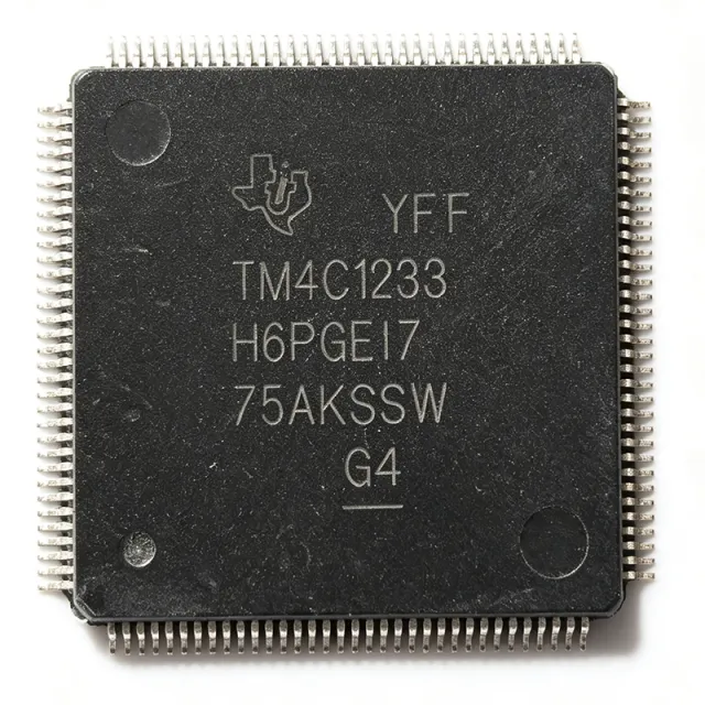
The Texas Instruments TM4C1233H6PGE is a 32-bit Arm Cortex-M4F microcontroller running at 80 MHz with 256 KB flash, 32 KB SRAM, dual CAN 2.0 controllers, RTC, and USB device support, housed in a 144-pin LQFP (20x20 mm) package. A microcontroller unit (MCU) is a single-chip computer that integrates a processor core, memory, and peripherals on one die. Within the semiconductor hierarchy, the TM4C1233H6PGE belongs to the 32-bit embedded microcontroller class, part of the Tiva C Series TM4C123x family built on the Arm Cortex-M4F architecture, which adds a hardware single-precision FPU, DSP instructions, and a Memory Protection Unit (MPU) on top of the standard Cortex-M core. Key features include the 80 MHz core with integrated FPU and MPU, 256 KB of on-chip flash with in-system programming support, 32 KB of SRAM, and a rich peripheral set: up to two CAN 2.0 controllers, USB 2.0 device, multiple UART, SSI, and I2C modules, 12-bit ADCs, PWM generators, and a battery-backed hibernate module with real-time clock. This combination makes the device well suited to mixed-signal industrial control where deterministic real-time response and robust fieldbus connectivity are required. Technically, the device uses the Tiva C Series 123x platform with a nested vectored interrupt controller (NVIC), SysTick timer, and both a precision internal oscillator and main oscillator inputs. Flash-based memory supports firmware updates via CAN or UART bootloaders, easing field maintenance in deployed equipment. Typical applications cited by TI include remote monitoring, electronic point-of-sale machines, test and measurement equipment, network appliances and switches, factory automation, HVAC and building control, and fire and security systems. A key design consideration is SRAM budgeting: enabling USB stacks and RTOS middleware can consume several kilobytes of the 32 KB SRAM, so applications needing more headroom should evaluate the TM4C123GH6PGE variant or the TM4C129x class. This page synthesizes verified distributor data, drop-in same-family alternatives, pricing, and practical design notes not found in the manufacturer datasheet alone.

USD $7.15 اتصل بنا
TM4C1237H6PZI - 80MHz ARM Cortex-M4F MCU 256KB Flash | TI
TM4C1237H6PZI

TM4C1237H6PZI - 80MHz ARM Cortex-M4F MCU 256KB Flash | TI

The Texas Instruments TM4C1237H6PZI is a 32-bit ARM Cortex-M4F microcontroller running at up to 80 MHz, integrating 256 KB of single-cycle Flash and 32 KB of single-cycle SRAM in a 100-pin LQFP (PZ) package. The part integrates a Floating-Point Unit (FPU) for single-precision IEEE 754 math, a memory protection unit, plus Tiva C Series connectivity peripherals including CAN 2.0, USB 2.0 (full-speed), and a real-time clock (RTC) with Hibernation module. An ARM Cortex-M4F microcontroller is a 32-bit MCU core built around the ARMv7-M architecture with hardware single-precision floating-point support, Thumb-2 instruction set, deterministic interrupt handling (NVIC), and tightly-coupled low-latency memory interfaces. In the broader taxonomy, the Cortex-M4F belongs to: Cortex-M4 -> Cortex-M family -> ARMv7-M processors -> 32-bit MCU -> microcontroller -> embedded processor -> semiconductor. Tiva C Series MCUs sit in TI's general-purpose 32-bit MCU portfolio, alongside MSP432, Sitara, and Hercules safety MCUs. Key features of the TM4C1237H6PZI include 8 UART, 4 SSI/SPI, 4 I2C, 2 CAN, 1 USB, two 12-bit 1-MSPS ADC modules (totaling up to 24 channels), six 64-bit and six 32-bit general-purpose timers, eight PWM outputs, three quadrature encoder interfaces, and a low-pin-count LCD interface on related derivatives. The 80-MHz system clock and single-cycle memory accesses deliver 100 DMIPS of throughput, while the integrated FPU accelerates DSP and control-loop math. Typical applications span industrial remote monitoring, electronic point-of-sale machines, test and measurement equipment, network appliances and switches, factory automation, HVAC and building control, gaming equipment, transportation, and fire/security systems. The combination of CAN and USB makes it a strong fit for industrial gateways; the RTC plus Hibernation module supports battery-backed timekeeping for metering. When designing with this part, ensure the LDO and I/O supply rails are sequenced within the datasheet limits, observe the 100-pin LQFP 1.4 mm thickness for mechanical clearance, and validate that the application's pin multiplexing matches the selected peripheral set.

طلب عرض سعر اتصل بنا
TM4C123GE6PZT7R - 80MHz ARM Cortex-M4F MCU, 128KB Flash | TI
TM4C123GE6PZT7R

TM4C123GE6PZT7R - 80MHz ARM Cortex-M4F MCU, 128KB Flash | TI

The Texas Instruments TM4C123GE6PZT7R is an ARM Cortex-M4F based Tiva C Series microcontroller running at 80 MHz with a single-cycle Floating Point Unit (FPU), integrating 128 KB of single-cycle Flash and 32 KB of single-cycle SRAM into a 100-pin LQFP package. Its Cortex-M4F core implements the Thumb-2 instruction set, deterministic nested vectored interrupt controller (NVIC), and hardware divide, single-cycle multiply, and saturated math support for DSP-style operations on a microcontroller footprint. The device is built on a 1.2 V internal core with 3.3 V I/O rails. A microcontroller (MCU) is a single-chip computer integrating a CPU core, volatile and non-volatile memory, and a rich set of programmable peripherals intended for embedded control. The Cortex-M4F class sits in the hierarchy: Cortex-M4F -> Cortex-M series -> ARMv7-M architecture -> 32-bit RISC MCU -> embedded processor -> semiconductor device; the FPU suffix denotes the single-precision IEEE 754 floating point unit. TM4C123GE6PZT7R combines CPU, memory, analog, motion-control, and connectivity peripherals into one IC, replacing what historically required a microprocessor plus external peripherals. Key features include 8 UARTs, 4 I2C, 4 SSI/SPI, 2 CAN 2.0B, USB 2.0 Full-Speed Host/Device/OTG, a 12-bit ADC with 1 MSPS and up to 22 analog inputs, two analog comparators, four general-purpose 16/32-bit timers, two watchdog timers, an Hibernation module with RTC, and a PWM block with fault inputs and dead-band generators. Operating voltage spans 3.15 V to 3.63 V with an LDO-derived 1.2 V core; the MCU is qualified for the industrial -40 °C to +85 °C range. Typical applications include industrial remote monitoring, electronic point-of-sale (POS) terminals, test and measurement front-ends, network appliances and switches, factory automation controllers, HVAC and building-control systems, gaming peripherals, motion-control hobby servos, and lighting controllers. Two integrated CAN controllers make it attractive for distributed industrial nodes and automotive body/motor subsystems. Designers should keep the analog and digital supply rails well decoupled with 100 nF ceramic bypass capacitors placed within a few millimeters of each VDD pin, plus a bulk 10 uF near the regulator output. The 100-LQFP (14x14) package thermal resistance theta_JA of around 47 C/W allows full industrial operation without a heatsink; ensure unused debug and JTAG pins are pulled to defined states when not used to avoid floating-input current draw.

طلب عرض سعر اتصل بنا
TM4C1290NCPDTI3R - Tiva C Series 120MHz ARM Cortex-M4F MCU, 1MB Flash | TI
TM4C1290NCPDTI3R

TM4C1290NCPDTI3R - Tiva C Series 120MHz ARM Cortex-M4F MCU, 1MB Flash | TI

The Texas Instruments TM4C1290NCPDTI3R is a high-performance 32-bit ARM Cortex-M4F microcontroller from TI's Tiva C Series, featuring a 120MHz core with FPU, 1MB Flash, and 256KB SRAM, housed in a 128-pin TQFP (14x14 mm) package. The device integrates extensive connectivity including Ethernet MAC+PHY, USB 2.0, CAN, UART, I2C, and SPI, making it well suited for connected industrial and IoT embedded designs. What is an ARM Cortex-M4F microcontroller? An ARM Cortex-M4F microcontroller is a 32-bit MCU based on the ARM Cortex-M4 processor core with single-precision floating-point unit (FPU), DSP extensions, and a Nested Vectored Interrupt Controller (NVIC). The M4F sits in the Cortex-M family hierarchy above Cortex-M0/M0+ (low-power 8/16-bit class performance) and Cortex-M3 (basic 32-bit), delivering deterministic real-time performance with DSP-class signal processing capability. Microcontrollers occupy the embedded computing tier below microprocessors (MPUs) in the system-on-chip taxonomy, integrating CPU, memory, peripherals, and often connectivity IP into one package. Key features of the TM4C1290NCPDTI3R include: integrated 10/100 Ethernet MAC and PHY, USB 2.0 full-speed host/device/OTG, two CAN 2.0B controllers, eight UARTs, ten I2C, four SSI/SPI, a 12-bit 2MSPS ADC with up to 24 analog inputs, and a hibernation module with RTC. The on-chip memory of 1MB Flash and 256KB single-cycle SRAM supports data-logging buffers, TCP/IP stacks (such as lwIP or TI's own NDK), and real-time control loops without external memory in many designs. The 16-bit CRC engine and AES/DES/SHA crypto accelerators (via the TivaWare library) are commonly leveraged for secured connectivity. Typical applications include industrial Ethernet gateways, PLC modules, networked sensors, building automation controllers, USB host peripherals (printers, scanners, POS terminals), automotive telematics, smart energy and smart grid endpoints, and SCADA remote terminal units (RTUs). The wide 3.3V I/O and integrated PHY reduce external BOM for cost-sensitive connected designs. When designing with this MCU, pay close attention to the TQFP-128 thermal performance at high CPU loading. Validate that the hibernation current budget meets battery-backed RTC requirements, and ensure PCB layout keeps the Ethernet differential pairs length-matched within datasheet tolerances. This page synthesizes distributor pricing, drop-in Tiva C alternatives, and practical design guidance not found in the manufacturer datasheet alone.

طلب عرض سعر اتصل بنا
TM4C1294NCPDTI3 - 120MHz Cortex-M4F MCU 1MB Flash | TI
TM4C1294NCPDTI3

TM4C1294NCPDTI3 - 120MHz Cortex-M4F MCU 1MB Flash | TI

The Texas Instruments TM4C1294NCPDTI3 is a 32-bit ARM Cortex-M4F microcontroller from the Tiva C Series operating at up to 120 MHz, with 1 MB of flash memory and 256 KB of SRAM, housed in a 128-pin TQFP (14x14 mm) surface-mount package. It integrates an Ethernet MAC with PHY, USB 2.0 Host/Device/OTG, and a rich serial-peripheral set aimed at highly connected IoT designs. A microcontroller (MCU) is a compact integrated circuit that governs specific operations in embedded systems, combining a processor core, memory, and programmable peripherals on a single die. In the product hierarchy, the TM4C1294NCPDTI3 sits within ARM Cortex-M4F core -> Tiva C Series -> TM4C129x family, and it is code-compatible across the Tiva C lineup, letting designers scale designs without rewriting firmware. Key features include the integrated 10/100 Ethernet MAC+PHY for direct network attachment without an external PHY, dual 12-bit ADCs for analog acquisition, and multiple UART, I2C, SPI, and CAN channels. The Cortex-M4F core adds a hardware floating-point unit (FPU), DSP instructions, and a memory protection unit (MPU) for firmware reliability. The industrial temperature grade covers -40C to +85C. Architecturally, the device pairs the 120 MHz M4F pipeline with 256 KB of on-chip SRAM and 1 MB of flash, a JTAG/SWD debug interface, and TI's TivaWare peripheral driver library. The DSP/FPU acceleration enables real-time control loops and digital signal processing without an external co-processor, while the MPU helps isolate critical code regions in safety-conscious firmware architectures. Typical applications include industrial automation nodes, IoT gateways, building automation and smart-grid equipment, networked control systems, and motor control. The integrated Ethernet MAC+PHY removes external components in many designs, cutting BOM cost and board area. Design consideration: decouple all VDD and VDDA pins with low-ESR ceramic capacitors placed close to the package, follow datasheet guidance for the 1.2V core regulator, and exploit low-power sleep modes in energy-sensitive nodes. This page synthesizes distributor pricing, verified drop-in alternatives, and practical design notes not found in the manufacturer datasheet.

طلب عرض سعر اتصل بنا
TM4E1231H6ZRBI - Tiva C ARM Cortex-M4 MCU 80MHz 256KB BGA | Texas Instruments
TM4E1231H6ZRBI

TM4E1231H6ZRBI - Tiva C ARM Cortex-M4 MCU 80MHz 256KB BGA | Texas Instruments

The Texas Instruments TM4E1231H6ZRBI is a 32-bit ARM Cortex-M4F microcontroller from the Tiva C (TM4C) Series featuring an 80 MHz core with Floating Point Unit, 256 KB single-cycle Flash, and 32 KB SRAM, packaged in a 157-ball BGA (ZRB package). The part integrates a high-performance analog comparator, two 12-bit ADC modules, multiple UART/SPI/I2C interfaces, and a full-speed USB 2.0 OTG controller with dedicated DMA, suited for industrial control and connectivity-rich embedded designs. An ARM Cortex-M4F MCU is a 32-bit microcontroller that adds a single-precision IEEE 754 Floating Point Unit and DSP extensions to the standard Cortex-M4 architecture. Within the broader taxonomy, this places it as a microcontroller -> embedded processor -> semiconductor device, the same family that includes Cortex-M0/M0+ low-end parts and Cortex-M7 high-performance parts. The 'F' suffix specifically denotes the FPU which is essential for sensor-fusion math, motor-control PI loops, and digital signal processing without integer-only precision loss. Key features include 256 KB Flash with pre-fetch buffer to minimize instruction stalls, 32 KB SRAM with byte-access arbitration, two 12-bit ADC modules each supporting up to 1 MSPS with 12 analog input channels, two CAN 2.0 A/B controllers, a USB OTG full-speed controller with ULPI option, an Ethernet MAC with 1588 timestamp support, and an integrated hibernation module for ultra-low-power battery-backed operation drawing as little as 1.6 uA on VBAT. Architecturally the TM4E1231H6ZRBI uses the Tiva C Series design philosophy combining ARM Cortex-M4F processing with a peripheral-rich pin mux that allows nearly every GPIO to map to alternate functions such as timers, QEI, PWM, and serial interfaces. The device is manufactured on a mature 65 nm process that delivers predictable MHz/mW ratios and supports industrial-grade temperature ranges. Typical applications include industrial motion control, USB-connected human-interface devices, building automation gateways, and factory sensor hubs. The combination of CAN 2.0B, Ethernet, and USB makes the part a strong fit for industrial IoT edge nodes that must bridge legacy field buses with TCP/IP networks. When designing with this device, pay close attention to the BGA157 substrate and use at least 4-layer PCB stack-up with microvia or via-in-pad technology to escape the dense ball grid. Allocate decoupling capacitance directly under the BGA to suppress switching transients during high-speed serial bursts. This page synthesizes current distributor pricing, BGA157 drop-in equivalents, and practical PCB layout guidance not found in the manufacturer datasheet.

طلب عرض سعر اتصل بنا
TM4E123GH6ZRBI7 - 80MHz ARM Cortex-M4F MCU, 256KB Flash | TI
TM4E123GH6ZRBI7

TM4E123GH6ZRBI7 - 80MHz ARM Cortex-M4F MCU, 256KB Flash | TI

The Texas Instruments TM4E123GH6ZRBI7 is a 32-bit ARM Cortex-M4F microcontroller from the Tiva C Series with an 80 MHz CPU, 256 KB single-cycle Flash, and 32 KB single-cycle SRAM, packaged in a 157-ball BGA (ZRBI). It includes a floating-point unit, a deterministic interrupt controller, and a rich peripheral set for industrial and consumer embedded applications. Key features include 8 UARTs, 4 I2C modules, 4 SSI/SPI controllers, 2 CAN 2.0 A/B controllers, a 12-bit 2-MSPS ADC with 24 analog inputs, two analog comparators, and a 16-bit PWM timer block with up to 32 PWM outputs. The device operates from 3.3 V (LDO regulation on-chip), supports industrial -40C to +85C temperature ranges, and integrates a JTAG/SWD debug interface. The 157-ball BGA package provides compact routing for high-pin-count designs. The TM4E123GH6ZRBI7 sits within the broader category hierarchy: ARM Cortex-M4F microcontroller -> ARM Cortex-M -> 32-bit microcontroller (MCU) -> microcontroller -> embedded processor -> semiconductor. This taxonomy helps engineers locate the part within the TI ecosystem and competing Cortex-M portfolios from NXP, STMicroelectronics, and Microchip. The architecture combines ARM Cortex-M4F core with TI's peripheral driver library and StellarisWare-compatible APIs. The deterministic interrupt controller provides 7 priority levels with tail chaining, reducing interrupt latency for real-time control. Hardware CRC and a random-number generator support communications protocols requiring data integrity verification. Typical applications include industrial motor control, factory automation, building HVAC, programmable logic controllers (PLCs), sensor aggregation hubs, and human-machine interface (HMI) panels. The 80 MHz core with FPU delivers sufficient throughput for closed-loop PID control while the BGA package suits space-constrained PCB designs with high I/O density. When designing with this part, ensure the BGA's thermal vias are properly stitched to internal ground planes for heat dissipation. Allocate sufficient PCB layers for signal escape routing on the 157-ball array, and use the on-chip LDO regulator mode by tying the VDD25 rail to the internal 2.5 V output. This page synthesizes distributor pricing, drop-in Tiva C Series alternatives, and practical design notes beyond the manufacturer datasheet, giving engineers a single source for selection and sourcing decisions.

طلب عرض سعر اتصل بنا
TMS320F241PG - 16-Bit 20MHz DSP with Flash | Texas Instruments
TMS320F241PG

TMS320F241PG - 16-Bit 20MHz DSP with Flash | Texas Instruments

The Texas Instruments TMS320F241PG is a 16-bit fixed-point digital signal processor with a 20 MHz C2xx CPU, 16 KB of on-chip flash memory, and a 64-pin QFP package measuring 14 mm by 20 mm. It combines fixed-point signal-processing performance with embedded flash memory in a surface-mount controller package designed for real-time control and DSP applications. A digital signal processor, or DSP, is a semiconductor optimized to execute mathematical operations on sampled data efficiently. A fixed-point DSP represents numerical values as integers and scaled fractional quantities, making it well suited to control loops, filtering, waveform generation, motor regulation, and industrial automation. The TMS320F241 belongs to the C2000 family of DSP controllers, which combines signal-processing capability with embedded control peripherals. The verified device description identifies a 16-bit architecture operating at 20 MHz, with 16 KB of flash organized as 8K by 16 words. Its 64-QFP package supports compact surface-mount assembly while providing a larger pin count than the QFP packages commonly used for small microcontrollers. The exact instruction-cycle time is stated in the retrieved technical material as 50 ns, which is consistent with a 20 MHz operating rate. The C2xx CPU core provides the computational foundation for digital filtering, control calculations, and fixed-point algorithms. Because the device includes embedded flash, a complete application can store its program code on the DSP itself rather than depending on an external program-memory device. This integration can simplify hardware and firmware organization in dedicated control equipment, although memory-intensive, multi-stage signal-processing designs must still evaluate the available 16 KB capacity carefully. Typical applications include digital motor control, industrial power conversion, servo and position control, embedded instrumentation, and real-time signal conditioning. Its 20 MHz rate and fixed-point architecture are especially useful in control loops where deterministic arithmetic and compact embedded code are more important than floating-point performance or a large general-purpose software ecosystem. Designers should review the manufacturer datasheet for the exact pin assignments, peripheral allocation, electrical limits, timing requirements, and external interface configuration. PCB layout should provide suitable decoupling at the supply pins and preserve clean signal routing, particularly when the DSP drives converters, sensors, or communication interfaces. Legacy software and peripheral differences must also be evaluated before migration to a newer C2000 device. This page combines the verified distributor and manufacturer references with practical guidance for controller selection, replacement assessment, PCB reuse, and real-time DSP implementation. It distinguishes confirmed specifications from data that still requires confirmation, helping engineers make sourcing and design decisions without relying on unverified parametric claims.

طلب عرض سعر اتصل بنا
TMS320F2800152-Q1 - 100MHz C2000 MCU, 64KB Flash | TI
TMS320F2800152-Q1

TMS320F2800152-Q1 - 100MHz C2000 MCU, 64KB Flash | TI

The Texas Instruments TMS320F2800152-Q1 is an automotive-qualified C2000 real-time microcontroller featuring a 32-bit TMS320C28x core running at 100 MHz, 64 KB (32K x 16) of on-chip flash memory, integrated CAN-FD, and lockstep functional-safety capability rated ASIL B. It is offered in a 32-pin VQFN (5x5 mm) package (ordering part F2800152QRHBRQ1). A real-time microcontroller (MCU) is a single-chip embedded processor that executes control loops with deterministic, ultra-low latency. Within the power-management hierarchy, the C2000 family sits above generic MCUs by pairing a DSP-class C28x core with dedicated control peripherals such as high-resolution PWM, fast ADCs, and comparators, making it the de facto standard for digital power conversion and motor control. Key features include the cost-optimized F280015x architecture designed for power electronics, CAN-FD for automotive networking, lockstep core operation supporting ASIL B safety integrity levels, and AEC-Q100 automotive qualification (Q1). The 64 KB flash suits compact control firmware, while the C28x pipeline delivers deterministic interrupt latency essential for current-loop control at switching frequencies of 100 kHz and above. The device integrates the characteristic C2000 control-law accelerator ecosystem: ePWM modules, on-chip analog comparators, and serial communication peripherals. Combined with TI's C2000Ware and MotorControl SDK, engineers can deploy field-oriented motor control, LLC/PFC digital power supplies, and solar inverter control with minimal external components. Typical applications include automotive onboard chargers and DC-DC converters, traction-inverter auxiliary supplies, industrial servo drives, and high-density AC-DC power supplies where ASIL-rated safety and CAN-FD connectivity are required. Design consideration: budget the 64 KB flash carefully - C2000 math libraries and FOC stacks can exceed this footprint, so verify code size against the larger F280015x flash variants if your algorithm set grows.

طلب عرض سعر اتصل بنا
TMS320F2800153-Q1 - 120MHz C2000 MCU, ASIL-B | TI
TMS320F2800153-Q1

TMS320F2800153-Q1 - 120MHz C2000 MCU, ASIL-B | TI

The Texas Instruments TMS320F2800153-Q1 is an automotive-qualified C2000 real-time 32-bit microcontroller running at 120 MHz with 64 KB (32K x 16) of on-chip flash, HRPWM, CAN-FD, and lockstep CPU safety architecture rated ASIL B, housed in a 48-pin HTQFP (7x7 mm) package. It belongs to the cost-optimized F280015x family of ultra-low latency real-time MCUs designed for power electronics control. A real-time MCU is a class of 32-bit microcontroller that executes control-loop code deterministically with microsecond-scale interrupt latency. Within the power-management semiconductor hierarchy, it sits above analog controllers and below application processors, dedicated to closing high-frequency control loops such as digital power conversion and motor commutation. Key features include the C28x DSP core at 120 MHz, 64 KB flash with ECC, high-resolution PWM (HRPWM) for fine duty-cycle control in LLC and phase-shifted converters, CAN-FD for in-vehicle networking, and a lockstep CPU core with integrated safety mechanisms meeting ASIL B requirements of ISO 26262. The family is scalable: F2800152 through F2800157 share the same die, package, and pinout, differing mainly in flash memory size. Architecturally, the device combines the fixed-point C28x CPU with dedicated trigonometric math unit (TMU), CLA-style acceleration options, 12-bit ADCs, and ePWM modules that enable single-chip closure of current, voltage, and speed loops in digital power supplies, on-board chargers, and traction inverters. Typical applications include automotive on-board chargers (OBC), DC-DC converters, HEV/EV traction motor control, solar micro-inverters, and servo drives, where deterministic 100 kHz+ control loops and functional safety are mandatory. The CAN-FD interface connects directly to vehicle body and powertrain networks. Design tip: budget flash headroom of at least 20% above initial firmware size, or select the pin-compatible F2800154/155/156/157 variants with larger flash so an PCB respin is never needed. Prices as of 2026-08-28; see FAQ for current tier pricing.

طلب عرض سعر اتصل بنا