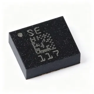
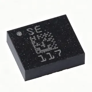
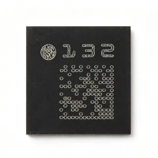
LSM6DSV320XTR - 6-Axis IMU ±320g ±4000dps AI Core | STMicroelectronics
MPN: LSM6DSV320XTR ✓ نشطLSM6DSV320XTR نظرة عامة
An IMU (Inertial Measurement Unit) is a micro-electromechanical system (MEMS) device that combines multiple sensing axes of accelerometer and gyroscope data into a single output. IMUs sit within the sensor hierarchy as motion sensors, which are a branch of MEMS semiconductors used in everything from smartphones to vehicles. The LSM6DSV320XTR belongs to the system-level category of "smart sensors" because it embeds a finite state machine (FSM) and a machine learning core (MLC) for on-device AI inference, eliminating the need for an external microcontroller to run motion classification algorithms.
Key features include ±320 g maximum accelerometer full-scale range, ±4000 dps gyroscope range, embedded machine learning core, adaptive self-configuration (ASC), and a 4.5 KB FIFO buffer for batched data streaming. The device operates from a 1.71V to 3.6V supply, draws only 2.9 µA in low-power mode, and exposes both I2C and SPI digital interfaces for flexible host integration. Operating temperature spans -40 °C to +85 °C, suiting industrial and consumer environments.
Technically, the LSM6DSV320XTR uses a dual-mass MEMS architecture to deliver high dynamic range without sacrificing low-g noise performance. The MLC and FSM allow engineers to run decision-tree and gesture-recognition models directly on-chip, dramatically reducing host MCU wake events and extending battery life in wearable applications. The 0.67 mA active supply current is competitive for always-on applications.
Typical use cases include car crash detection telemetry, wearables with embedded activity recognition, IoT vibration monitoring, and personal electronics with context-aware gesture input. The automotive-grade crash detection capability is unique in a sub-$10 IMU and addresses insurance telematics and event data recorder designs.
Design consideration: the dual-accelerometer topology requires attention to which chain is enabled in firmware; designers must select the appropriate full-scale range per sensing phase to avoid saturating the low-g channel during impact events. Decoupling capacitors should be placed within 2 mm of the supply pins.
This page synthesizes distributor pricing, drop-in alternatives, and practical design notes not found in the manufacturer datasheet.
بدائل مباشرة لـ LSM6DSV320XTR — نفس الحزمة، متوافق دبوس بدبوس. تُستثنى القطع ذات الحزم المختلفة التي تتطلب تعديل PCB.
الطرازات في هذه السلسلة
طرازات من نفس السلسلة متوافقة تمامًا مع LSM6DSV320XTR (نفس عامل الشكل والبصمة) — يختلف في Embedded Features, Package, Sensor Type, FIFO, Operating Temperature.
LSM6DSV320X
✅ بديل مباشر📋 بديل مرجعي (غير موجود في الكتالوج)
LSM6DSV320XTR
✅ بديل مباشرتواصل لمعرفة السعر
عرض ورقة البيانات ←LSM6DSO32XTR
✅ بديل مباشرتواصل لمعرفة السعر
عرض ورقة البيانات ←LSM6DSOXTR
✅ بديل مباشرتواصل لمعرفة السعر
عرض ورقة البيانات ←LSM6DSO32NTR
✅ بديل مباشر📋 بديل مرجعي (غير موجود في الكتالوج)
LSM6DSV320XTR الحدود القصوى والخصائص الكهربائية
| نوع المستشعر | Accelerometer, Gyroscope, Temperature (6-axis IMU) |
| نوع الخرج | I2C, SPI |
| Gyroscope Full-Scale Range | ±4000 dps |
| درجة حرارة التشغيل | -40 °C to +85 °C |
| جهد التغذية | 1.71 V to 3.6 V |
| Supply Current (low-power mode) | 2.9 µA |
| Supply Current (active) | 0.67 mA |
| FIFO Buffer | 4.5 KB |
| العلبة | LGA-14L (2.5x3x0.86 mm) |
| نوع التركيب | Surface Mount |
| Axes | X, Y, Z (both accelerometer and gyroscope) |
| Embedded Features | Finite State Machine (FSM), Machine Learning Core (MLC), Adaptive Self-Configuration (ASC) |
| حالة RoHS | Compliant |
| Lead-Free | Yes |
تكوين أطراف LSM6DSV320XTR
| دبوس 1 | VDD — Power supply (1.71V to 3.6V) |
| دبوس 2 | GND — Ground reference |
| دبوس 3 | RES — Reserved (connect to GND or leave NC per datasheet) |
| دبوس 4 | SDA/SDI — I2C data / SPI data input |
| دبوس 5 | SCL/SPC — I2C clock / SPI clock |
| دبوس 6 | CS — SPI chip select (active low) |
| دبوس 7 | INT1 — Interrupt 1 output |
| دبوس 8 | INT2 — Interrupt 2 output |
| دبوس 9 | SDO/SA0 — SPI data output / I2C address select |
| دبوس 10 | GND — Ground reference |
| دبوس 11 | RES — Reserved (connect per datasheet) |
| دبوس 12 | RES — Reserved (connect per datasheet) |
| دبوس 13 | GND — Ground reference |
| دبوس 14 | VDDIO — I/O voltage reference |
التطبيقات النموذجية
LSM6DSV320XTR مناسب لـ 6 التطبيقs: Automotive Crash Detection, Wearable Activity Recognition, Industrial Vibration Monitoring, Smartphone Context Awareness, IoT Gesture Recognition, Sports Impact Tracking.
Automotive Crash Detection
The LSM6DSV320XTR's ±320 g high-g accelerometer chain captures automotive crash-level events that saturate standard MEMS accelerometers. Its ±4000 dps gyroscope simultaneously records vehicle rotation during collision, enabling accurate crash severity classification for insurance telematics and event data recorders (EDR). The dual-chain topology means a single IMU replaces a low-g + high-g two-IMU stack, simplifying BOM. Operates across -40°C to +85°C automotive temperature range. Designers can leverage the embedded FSM to trigger black-box recording only when impact thresholds are exceeded, reducing false-positive storage events and extending EDR flash endurance.
موصى به
Wearable Activity Recognition
The embedded Machine Learning Core (MLC) on the LSM6DSV320XTR executes decision-tree AI models directly on-chip, classifying activities such as walking, running, swimming, and sleeping without waking the application processor. This offloads always-on inference from the host MCU, reducing wrist-worn wearable power consumption by orders of magnitude. The 2.9 µA low-power current enables multi-month standby on small Li-ion cells. The high-g chain captures impact events like drop-and-pickup gestures. Reference ST application note gives ready-to-deploy MLC decision trees for fitness-band activity classification.
موصى به
Industrial Vibration Monitoring
The LSM6DSV320XTR's wide ±4000 dps gyroscope dynamic range captures high-RPM machinery vibration signatures that saturate lower-range IMUs. The 4.5 KB FIFO buffers batched sensor data, allowing the host MCU to sleep while vibration profiles accumulate - critical for predictive-maintenance IoT nodes that must operate for years on battery. The wide 1.71V-3.6V supply range accepts direct connection to lithium-thionyl-chloride primary cells common in remote industrial sensors. The MLC detects anomaly signatures on-chip, flagging only actionable events upstream.
موصى به
Smartphone Context Awareness
Smartphones leverage the LSM6DSV320XTR's MLC for screen-rotation, pocket detection, and step counting without CPU wake events. The I2C/SPI dual interface drops onto standard mobile sensor hubs without glue logic. Adaptive Self-Configuration (ASC) automatically tunes ODR and full-scale range based on detected motion context, optimizing power consumption dynamically. The 2.5x3 mm LGA-14 footprint fits compact handset PCB real estate. Per ST application note, the MLC decision trees for tilt, raise-to-wake, and shake gestures ship as ready-to-load firmware assets.
موصى به
IoT Gesture Recognition
The FSM and MLC cores on the LSM6DSV320XTR recognize air gestures, taps, and double-taps directly on-device, enabling touchless interfaces for smart-home IoT devices. Designers train custom gesture models using ST's MLC configuration tool without writing host-side code, dramatically accelerating prototyping. The high-g chain also detects device drop impacts, triggering protective actions like SSD park-and-shutdown. The wide supply range (1.71V-3.6V) accepts battery voltages from coin cells to Li-ion packs across diverse IoT form factors.
موصى به
Sports Impact Tracking
Action cameras, smart mouthguards, and athletic impact monitors leverage the LSM6DSV320XTR's ±320 g accelerometer range to record head-impact accelerations in contact sports like football, hockey, and boxing. The 4000 dps gyroscope simultaneously captures rotational acceleration linked to concussion risk. The 2.9 µA low-power current supports multi-day tournament monitoring without recharge. ST's MLC decision trees can pre-classify impact severity on-device, transmitting only high-severity events over Bluetooth to conserve bandwidth and battery.
موصى به
ملخص المنتجات الموصى بها
بيانات مرجعية هندسية لـ LSM6DSV320XTR — المقارنة وإرشادات التصميم ومعلومات الامتثال.
دليل الاختيار
المقارنة مع البدائل
| المعامل | هذا المنتج | LSM6DSV320X | LSM6DSO32XTR | LSM6DSOXTR | LSM6DSO32NTR |
|---|---|---|---|---|---|
| Package | LGA-14L (2.5x3x0.86 mm) | LGA-14L (2.5x3x0.86 mm) - same | LGA-14L (2.5x3 mm) - same family | LGA-14L (2.5x3 mm) - same family | LGA-14L (2.5x3 mm) - same family |
| Brand | STMicroelectronics | STMicroelectronics | STMicroelectronics | STMicroelectronics | STMicroelectronics |
| Accelerometer Max FSR | ±320 g (high-g chain) | ±320 g - same | ±32 g - lower | ±16 g - lower | ±32 g - lower |
| Gyroscope Max FSR | ±4000 dps | ±4000 dps - same | ±2000 dps - lower | ±2000 dps - lower | ±2000 dps - lower |
| Supply Current (active) | 0.67 mA | 0.67 mA - same | 0.55 mA - lower | 0.55 mA - lower | 0.55 mA - lower |
| Embedded MLC/AI | Yes (FSM + MLC + ASC) | Yes - same | Yes | Yes | Yes |
| Supply Voltage | 1.71V to 3.6V | 1.71V to 3.6V - same | 1.71V to 3.6V - same | 1.71V to 3.6V - same | 1.71V to 3.6V - same |
| FIFO Buffer | 4.5 KB | 4.5 KB - same | 4.5 KB - same | 4.5 KB - same | 4.5 KB - same |
| Unit Price (qty 1) | $8.46 | $8.46 (same die) | ~$5.50 - lower | ~$4.20 - lower | ~$5.50 - lower |
أبرز الفروقات
- Highest accelerometer FSR in LSM6 family (مقابلLSM6DSOXTR)
- Embedded Machine Learning Core on-chip (مقابلLSM6DSO32XTR)
- Wider gyroscope dynamic range than predecessors (مقابلLSM6DSO32NTR)
ملاحظات التصميم
Estimated: at 3.6V supply and 0.67 mA active current, the device draws approximately 2.4 mW continuously during full-rate sampling. In low-power mode at 2.9 µA, the device draws approximately 10 µW - enabling multi-year battery life for IoT sensor nodes with duty-cycled operation. Designers should place a 100 nF X7R decoupling capacitor within 2 mm of the VDD pin and a 1 µF bulk capacitor on VDDIO to suppress supply transients during high-dynamic-range impact events.
Critical: do not exceed 3.6V on VDD or expose the device to ESD beyond ±2000V HBM without external protection. The high-g ±320 g chain saturates on routine motion events; firmware must gate high-g activation behind a low-g trigger to avoid capturing noise as crash data. Reserved pins (RES) must be connected per datasheet instructions - typically to GND - rather than left floating, as floating reserved pins can trigger inadvertent interrupts.
Recommended: keep the LGA-14 land area free of signal traces under the package to maximize thermal dissipation and reduce mechanical stress on solder balls. Route I2C/SPI traces as short as possible (<25 mm) with 4.7 kohm pull-ups on SDA/SCL. Place the INT1/INT2 traces away from noisy switching power lines to prevent false interrupt triggering. The exposed die pad pads on the package underside must be soldered to the PCB ground pour for proper thermal and electrical reference.
معلومات الامتثال
RoHS and lead-free status confirmed from JLCPCB and Newark distributor listings. AEC-Q100 automotive qualification status not explicitly stated in retrieved data - verify against ST automotive product family if required for vehicle applications.