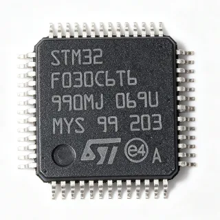
MC9S12C64VFAE - 16-Bit HCS12 MCU, 64KB Flash, LQFP-48 | NXP
MPN: MC9S12C64VFAE ✗ انتهى عمره الإنتاجيMC9S12C64VFAE نظرة عامة
A microcontroller (MCU) is a single-chip computer that integrates a CPU core, program memory (Flash/ROM), working memory (RAM), and a rich set of peripheral interfaces such as timers, ADCs, communication ports, and general-purpose I/O. The HCS12 family sits in the 16-bit microcontroller tier of NXP's automotive product tree: HCS12 CPU -> S12C sub-family -> 16-bit MCU -> automotive microcontroller -> embedded processor -> semiconductor. The 16-bit data path gives a meaningful step up from 8-bit MCUs in code density, arithmetic performance, and peripheral integration while keeping peripheral programming simple.
Key features of the MC9S12C64VFAE include 64KB of Flash program memory, 4KB of RAM, 31 general-purpose I/O pins, an on-chip bandgap-based voltage regulator that derives the core VDD from a 2.97V to 5.5V external supply, an integrated phase-locked loop (PLL) for flexible clocking, multiple serial communication interfaces (SCI, SPI), timers, an 8/10-bit ADC, and a CAN 2.0 A/B controller for in-vehicle networking. The device supports background debug mode (BDM) for non-intrusive in-circuit development.
The S12C architecture uses a 16-bit HCS12 core with a Von Neumann bus and a unified memory map, simplifying C-code development with NXP's CodeWarrior and the newer S32 Design Studio toolchains. The on-chip voltage regulator allows operation from a single 5V automotive rail while generating the lower core voltage internally, reducing BOM cost and PCB complexity.
Typical applications include body electronics controllers (door modules, seat controllers, mirror modules), CAN node endpoints in automotive networks, industrial sensor hubs, HVAC controllers, lighting controllers, general-purpose 16-bit control, and appliance control boards that benefit from automotive-grade peripherals such as CAN and a wide supply range.
When designing with the MC9S12C64VFAE, place the four VDD/VSS bulk capacitors specified in the datasheet close to their respective pins to ensure stable regulator operation. Always use the BDM interface for firmware development; the BDM pinout is part of the 48-pin LQFP pinmap and must be reserved for programming/debug access.
This page synthesizes distributor pricing, drop-in alternatives drawn from the same NXP S12C family and other sources, and practical design notes not found in the manufacturer datasheet alone.
بدائل مباشرة لـ MC9S12C64VFAE — نفس الحزمة، متوافق دبوس بدبوس. تُستثنى القطع ذات الحزم المختلفة التي تتطلب تعديل PCB.
الطرازات في هذه السلسلة
طرازات من نفس السلسلة متوافقة تمامًا مع MC9S12C64VFAE (نفس عامل الشكل والبصمة) — يختلف في PLL, On-chip Voltage Regulator, Program Memory Size, RAM Size, ADC.
MC9S12C64CFAE
✅ بديل مباشر📋 بديل مرجعي (غير موجود في الكتالوج)
MC9S12C64MFAE
✅ بديل مباشرتواصل لمعرفة السعر
عرض ورقة البيانات ←MC9S12C96CFAE557
✅ بديل مباشرتواصل لمعرفة السعر
عرض ورقة البيانات ←MC9S12GC64CFAE
✅ بديل مباشرتواصل لمعرفة السعر
عرض ورقة البيانات ←MC9S12C32VFAE16
✅ بديل مباشر ⚠️ مواصفات غير مُتحقق منهاتواصل لمعرفة السعر
عرض ورقة البيانات ←MC9S12C64VFAE الحدود القصوى والخصائص الكهربائية
| Core | HCS12 |
| عرض ناقل البيانات | 16 bit |
| Program Memory Size | 64 KB Flash |
| RAM Size | 4 KB |
| أقصى تردد للساعة | 25 MHz |
| Supply Voltage Range | 2.97 V to 5.5 V (external); internal Vreg generates core VDD |
| I/O Pins | 31 |
| ADC | 8/10-bit on-chip |
| Communication Interfaces | CAN 2.0 A/B, SCI (UART), SPI |
| Timers | 16-bit Enhanced Capture Timer (ECT) and others (per datasheet) |
| On-chip Voltage Regulator | Yes (bandgap-based) |
| PLL | Yes (phase-locked loop) |
| Debug Interface | Background Debug Mode (BDM) |
| العلبة | 48-pin LQFP (7x7 mm) |
| نوع التركيب | Surface Mount |
| درجة حرارة التشغيل | -40C to +105C |
تكوين أطراف MC9S12C64VFAE
| دبوس 1 | VDDX — External power supply (5 V typical, 2.97-5.5 V range) |
| دبوس 2 | VSSX — Ground for I/O supply |
| دبوس 3 | PP0/KWP0/PWM0 — GPIO with key wakeup and PWM capability |
| دبوس 4 | PP1/KWP1/PWM1 — GPIO with key wakeup and PWM capability |
| دبوس 5 | PP2/KWP2/PWM2 — GPIO with key wakeup and PWM capability |
| دبوس 6 | PP3/KWP3/PWM3 — GPIO with key wakeup and PWM capability |
| دبوس 7 | PP4/KWP4/PWM4 — GPIO with key wakeup and PWM capability |
| دبوس 8 | PP5/KWP5/PWM5 — GPIO with key wakeup and PWM capability |
| دبوس 9 | PP6/KWP6/PWM6 — GPIO with key wakeup and PWM capability |
| دبوس 10 | PP7/KWP7/PWM7 — GPIO with key wakeup and PWM capability |
| دبوس 11 | PT0/IOC0 — Timer/GPIO |
| دبوس 12 | PT1/IOC1 — Timer/GPIO |
| دبوس 13 | PT2/IOC2 — Timer/GPIO |
| دبوس 14 | PT3/IOC3 — Timer/GPIO |
| دبوس 15 | PT4/IOC4 — Timer/GPIO |
| دبوس 16 | PT5/IOC5 — Timer/GPIO |
| دبوس 17 | PT6/IOC6 — Timer/GPIO |
| دبوس 18 | PT7/IOC7 — Timer/GPIO |
| دبوس 19 | PAD0/AN0 — Port AD with ADC analog input |
| دبوس 20 | PAD1/AN1 — Port AD with ADC analog input |
| دبوس 21 | PAD2/AN2 — Port AD with ADC analog input |
| دبوس 22 | PAD3/AN3 — Port AD with ADC analog input |
| دبوس 23 | PAD4/AN4 — Port AD with ADC analog input |
| دبوس 24 | PAD5/AN5 — Port AD with ADC analog input |
| دبوس 25 | PAD6/AN6 — Port AD with ADC analog input |
| دبوس 26 | PAD7/AN7 — Port AD with ADC analog input |
| دبوس 27 | VDDR — Power supply for digital I/O (regulator input) |
| دبوس 28 | VSS — Ground |
| دبوس 29 | VDD — Internal regulator output (core supply) |
| دبوس 30 | VSS — Ground |
| دبوس 31 | BKGD — Background Debug Mode (BDM) pin |
| دبوس 32 | RESET — Reset input (active low) |
| دبوس 33 | TEST — Test mode pin (tie to VSS in normal operation) |
| دبوس 34 | XCLKS — Oscillator clock select |
| دبوس 35 | XTAL — Crystal oscillator input |
| دبوس 36 | EXTAL — Crystal oscillator output / external clock input |
| دبوس 37 | VSSPLL — PLL ground |
| دبوس 38 | VDDPLL — PLL supply |
| دبوس 39 | CANRX — CAN receive input |
| دبوس 40 | CANTX — CAN transmit output |
| دبوس 41 | SCIRXD — SCI (UART) receive input |
| دبوس 42 | SCITXD — SCI (UART) transmit output |
| دبوس 43 | PS0/MISO — SPI0 master-in slave-out / GPIO |
| دبوس 44 | PS1/MOSI — SPI0 master-out slave-in / GPIO |
| دبوس 45 | PS2/SCK — SPI0 clock / GPIO |
| دبوس 46 | PS3/SS — SPI0 slave select / GPIO |
| دبوس 47 | VDDX — External power supply (5 V typical) |
| دبوس 48 | VSSX — Ground for I/O supply |
التطبيقات النموذجية
MC9S12C64VFAE مناسب لـ 6 التطبيقs: Automotive Body Control Module (BCM), CAN Node Endpoints (Sensor / Actuator Modules), Industrial Sensor Hubs and Controllers, HVAC and Climate Control Units, Lighting Controllers (Interior and Exterior LED), Appliance and White-Goods Control Boards.
Automotive Body Control Module (BCM)
The MC9S12C64VFAE is widely used in body control modules where it drives loads such as door locks, mirror adjustments, seat motors, and lighting. Its 16-bit HCS12 core at 25 MHz easily handles multiplexed switch scanning, PWM-driven actuator control, and CAN 2.0 A/B messaging with other ECUs on the vehicle bus. The on-chip bandgap regulator accepts a 5 V automotive rail directly, eliminating an external 3.3 V LDO and trimming BOM cost. With 31 GPIO and an 8/10-bit ADC, the part reads multiple switch and sensor inputs while issuing actuator commands, and its -40C to +105C temperature range covers under-hood and cabin environments.
موصى به
CAN Node Endpoints (Sensor / Actuator Modules)
As a CAN 2.0 A/B node, the MC9S12C64VFAE integrates cleanly into automotive sensor clusters such as door modules, mirror controllers, and lighting nodes. The integrated msCAN module, acceptance filters, and 16-bit timers make event-driven CAN networking straightforward, while the 64 KB Flash holds both the CAN stack and application code. Its 48-pin LQFP footprint is shared across the S12C family, so designers can move to larger-memory (MC9S12C96CFAE) or scaled-down (MC9S12C32VFAE16) parts without PCB rework when firmware size changes.
موصى به
Industrial Sensor Hubs and Controllers
Outside the car, the MC9S12C64VFAE serves in PLC I/O modules, HVAC controllers, and industrial sensor hubs that need a robust 16-bit core with on-chip CAN. Its 2.97 V to 5.5 V supply tolerance suits 24 V industrial buses stepped down to 5 V, while the 8/10-bit ADC digitizes analog sensors (temperature, pressure, current). The PLL enables flexible bus-clock tuning, and BDM lets field engineers re-flash firmware without removing the module. The wide -40C to +105C operating range supports outdoor enclosures and factory-floor deployment.
موصى به
HVAC and Climate Control Units
In climate-control units, the MC9S12C64VFAE runs the closed-loop control algorithms for blower speed, mixed-air damper position, and temperature regulation. The Enhanced Capture Timer (ECT) drives PWM outputs for motor control, while the on-chip ADC reads NTC thermistors for cabin and ambient temperature. Because the part integrates a CAN controller, it can be slaved to the vehicle's HVAC master controller or, in industrial settings, operate as a standalone controller with a discrete user interface.
موصى به
Lighting Controllers (Interior and Exterior LED)
The MC9S12C64VFAE drives LED matrix controllers, ambient interior lighting, and exterior lamp modules using its timer PWM channels. The 16-bit HCS12 core handles LIN/CAN command parsing, brightness ramps, and fault diagnostics. Its 31 GPIO and -40C to +105C temperature range allow it to be placed near power-MOSFET LED drivers in exterior lamp modules without thermal concerns. The on-chip Vreg simplifies PCB layout by removing the need for a separate logic-rail LDO.
موصى به
Appliance and White-Goods Control Boards
White-goods controllers (washing machines, dishwashers, ovens) benefit from the MC9S12C64VFAE's automotive-grade peripherals at industrial price points. The on-chip ADC scans motor-current shunts and temperature sensors, while PWM channels drive triacs or relay drivers. The CAN interface can connect to a home-appliance network or to a service tool for diagnostics. Its 48-pin LQFP is hand-solder-friendly for low-volume repair depots, an advantage over BGA alternatives.
موصى به
ملخص المنتجات الموصى بها
بيانات مرجعية هندسية لـ MC9S12C64VFAE — المقارنة وإرشادات التصميم ومعلومات الامتثال.
دليل الاختيار
المقارنة مع البدائل
| المعامل | هذا المنتج | MC9S12C64CFAE | MC9S12C64MFAE | MC9S12C96CFAE | MC9S12GC64CFAE | MC9S12C32VFAE16 |
|---|---|---|---|---|---|---|
| Package | LQFP-48 (7x7 mm) | LQFP-48 - same | LQFP-48 - same | LQFP-48 - same | LQFP-48 - same | LQFP-48 - same |
| Brand | NXP Semiconductors | NXP Semiconductors | NXP Semiconductors | NXP Semiconductors | NXP Semiconductors | NXP Semiconductors |
| Core | HCS12 (16-bit) | HCS12 | HCS12 | HCS12 | S12GC | HCS12 |
| Flash Memory | 64 KB | 64 KB | 64 KB | 96 KB | 64 KB | 32 KB |
| RAM | 4 KB | 4 KB | 4 KB | 4 KB | 4 KB | 2 KB |
| Operating Temperature | -40C to +105C (V-suffix) | 0C to +70C (C-suffix) | M-suffix grade (per NXP ordering info) | 0C to +70C (C-suffix) | 0C to +70C (C-suffix) | -40C to +105C (V-suffix) |
| Supply Voltage Range | 2.97 V to 5.5 V | 2.97 V to 5.5 V | 2.97 V to 5.5 V | 2.97 V to 5.5 V | 2.97 V to 5.5 V | 2.97 V to 5.5 V |
| On-chip CAN 2.0 A/B | Yes (msCAN) | Yes | Yes | Yes | Yes | Yes |
أبرز الفروقات
- Single-rail 2.97-5.5 V operation with on-chip Vreg (مقابلGeneric 16-bit MCU without integrated regulator)
- 16-bit HCS12 core with 64 KB Flash in LQFP-48 (مقابلMC9S12C32VFAE16 (32 KB Flash, same footprint))
- Integrated CAN 2.0 A/B with on-chip acceptance filters (مقابلMC9S12C-series devices without CAN)
ملاحظات التصميم
The MC9S12C64VFAE integrates a bandgap-based voltage regulator (Vreg) that converts the external VDDX/VDDR (2.97-5.5 V) to the internal core VDD. Place the four bulk/decoupling capacitors specified in the NXP S12C datasheet (typically 100 nF plus larger bulk values) directly at the VDDX, VDDR, VDD, and VSS pins to ensure regulator stability. Inadequate decoupling can cause erratic reset behavior or bus-clock jitter. Keep the VDDX trace short and wide.
Reserve the BKGD pin (BDM) and the RESET pin access at board edge or test pad for in-circuit firmware updates. The BKGD pin must be pulled up during reset per the S12C datasheet. Place the external crystal or resonator (XTAL/EXTAL) close to the MCU and shield it with a grounded guard ring to avoid injecting noise into the PLL. Keep the CANRX/CANTX traces short and route them as a differential pair to the CAN transceiver, with a 120-ohm termination at the bus ends.
Do not leave the TEST pin floating - it must be tied to VSS for normal operation per the NXP S12C datasheet, otherwise the part may enter test mode and not boot. The XCLKS pin must be configured correctly for the chosen oscillator topology (loop-controlled Pierce vs full-swing). When migrating between V-suffix and C-suffix S12C parts, re-validate the temperature profile because the C-suffix device does not operate at -40C and can fail to start up cold.
معلومات الامتثال
RoHS/lead-free status not found in the verified sources above; consult the NXP product page RoHS/REACH statement for the authoritative compliance data. AEC-Q100 grade not stated explicitly in the verified data; check the NXP qualification matrix for automotive-grade certification.