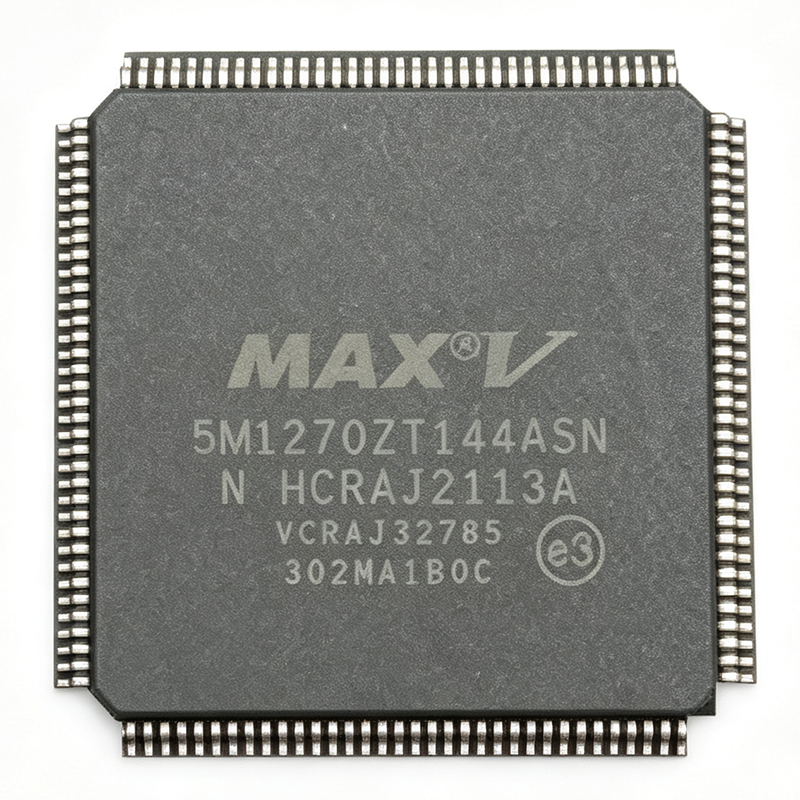
The 5M1270ZT144A5N is a 980-macro-cell CPLD from the Intel (formerly Altera) MAX V family, supplied in a 144-pin TQFP package with 114 user I/Os, a 201.1 MHz maximum internal operating frequency, a 1.8 V core supply, and MultiVolt I/O banks supporting 1.8 V, 2.5 V, 3.3 V, and 5.0 V. Its non-volatile flash configuration means it powers up ready to run with no external boot PROM. The part is active, RoHS compliant, and available on XAIPART with stock of 99,999 units, MOQ 1, priced from $22.50 at 1 piece down to $13.95 at 1,000 pieces as of 2026-09-12. This guide covers verified specifications, design-in practices, pinout highlights, drop-in alternatives within the same TQFP-144 footprint, and application scenarios from bus bridging to power sequencing.
Quick Answers: What Should Every Buyer and Engineer Know About the 5M1270ZT144A5N?
The 5M1270ZT144A5N belongs to the MAX V CPLD family and occupies the space between discrete 74-series logic and high-density FPGAs: CPLD -> programmable logic -> logic IC -> integrated circuit -> semiconductor. Each of its 980 macro cells combines a programmable AND/OR array with a flip-flop, and designs are synthesized from VHDL, Verilog, or schematic entry using the Quartus II / Quartus Prime toolset. Key verified specifications include:
| Parameter | Verified Value |
|---|---|
| Manufacturer | Altera (Intel) |
| Family | MAX V CPLD |
| Macro Cells | 980 (~2120 logic elements) |
| User I/Os | 114 |
| Max Operating Frequency | 201.1 MHz (5N speed grade) |
| Core Supply (VCCINT) | 1.8 V |
| I/O Supply (VCCIO) | 1.8 V / 2.5 V / 3.3 V / 5.0 V (MultiVolt) |
| User Flash Memory | 8 Kbits |
| Package | TQFP-144, surface mount |
| JTAG | Yes (IEEE 1149.1 boundary-scan) |
| On-chip Oscillator | Yes |
| RoHS | Compliant |
| Lifecycle | Active |
Availability: XAIPART lists 99,999 units in stock with MOQ 1. Pricing as of 2026-09-12: $22.50 (qty >= 1), $20.40 (qty >= 10), $17.85 (qty >= 100), $15.60 (qty >= 500), $13.95 (qty >= 1000). Distributor data as of 2026-09-06 shows active stock at DigiKey (part 544-3176-ND) and listings at Mouser and Octopart, with factory lead time typically 8 to 12 weeks for new orders.
Technical Guide: How Do You Select, Design In, and Program the 5M1270ZT144A5N?
Why Choose a Non-Volatile Flash CPLD?
Because configuration lives in on-chip non-volatile flash, the 5M1270ZT144A5N requires no external configuration PROM and powers up ready to run within microseconds. This simplifies the BOM, removes boot-time latency, and makes power-up behavior deterministic — a key advantage in power sequencing and safety-critical control loops. Compared to legacy MAX 7000 or MAX II parts, MAX V delivers up to 2x higher logic density per macro cell and adds 8 Kbits of user flash while keeping the same JTAG programming chain and pinout philosophy for backward-compatible boards.
Power Supply and Decoupling Design
The core runs from a single 1.8 V VCCINT rail. Each of the four I/O banks has its own VCCIO pin group (bank 1 at pin 9, bank 2 at pin 34, bank 3 at pins 52 and 72, bank 4 at pins 87 and 121 per the verified pinout), so you can mix 1.8 V, 2.5 V, 3.3 V, and 5.0 V interfaces on one device. Place 0.1 uF and 10 uF decoupling capacitors close to every VCCINT and VCCIO pin, and observe MultiVolt bank rules so that 5 V-tolerant inputs never exceed absolute maximum ratings.
Key Pins at a Glance
The TQFP-144 pinout is organized into four I/O banks plus power, ground, and JTAG functions. Functionally critical pins include the JTAG chain (TMS, TCK, TDI, TDO on pins 47–50), core supplies (VCCINT on pins 23, 78, 104), I/O bank supplies (VCCIO on pins 9, 34, 52, 72, 87, 121), and the configuration-related pins nCONFIG (136), nSTATUS (137), and CONF_DONE (138). Internal pull-up resistors and bus-hold circuitry eliminate external termination on many signal lines, reducing component count.
Programming Workflow
Design capture happens in Quartus II or Quartus Prime using VHDL, Verilog, or schematic entry. The toolchain compiles the design into a JIC or POF programming file, which is loaded in-system over the JTAG interface (IEEE 1149.1) using an Intel FPGA USB-Blaster, ByteBlasterMV, or compatible programmer. Because programming is in-system, logic changes that once required a PCB respin become a short recompile and JTAG flash update.
Package and Assembly Considerations
The TQFP-144 package is surface-mount but hand-solderable and socketable, unlike fine-pitch BGA alternatives. This makes the 5M1270ZT144A5N well suited to educational platforms, prototyping boards, and low-volume builds where BGA assembly is impractical.
Alternatives & Comparison: What Are the Drop-In Replacements for the 5M1270ZT144A5N?
The strongest drop-in replacements are other 5M1270ZT144 variants that share the same TQFP-144 footprint and 980-macro-cell core. The following alternatives are verified as pin-to-pin compatible in the same package:
| Parameter | 5M1270ZT144A5N | 5M1270ZT144A5G | 5M1270ZT144I7N |
|---|---|---|---|
| Package | TQFP-144 | TQFP-144 | TQFP-144 |
| Macro Cells | 980 | 980 | 980 |
| Speed Grade | A5 (5N) | A5G (slightly relaxed timing) | I7N (slower speed grade) |
| Temperature Grade | Standard (commercial) | [DATA_NEEDED: temperature grade of A5G] | Industrial (I7N) |
| Pin Compatibility | Reference | Pin-to-pin compatible | Pin-to-pin compatible |
| Core | MAX V 1.8 V flash CPLD | MAX V 1.8 V flash CPLD | MAX V 1.8 V flash CPLD |
Selection guidance: stay with the 5N speed grade (5M1270ZT144A5N) when your design relies on the verified 201.1 MHz maximum internal frequency; move to the 5M1270ZT144A5G if slightly relaxed timing is acceptable; choose the 5M1270ZT144I7N for industrial environments that require the industrial temperature grade. All three can be swapped without PCB rework. Cross-brand, the Lattice ispMACH 4000ZE family (for example LC4128ZE-5TN100C or LC4256ZE-8TN100C) is sometimes cited as a functional equivalent, but these are NOT drop-in replacements without PCB rework and pinout verification against the manufacturer datasheet.
Within the broader 5M1270Z device family, the 5M1270ZF256 (FBGA-256) and 5M1270ZF324 (FBGA-324) variants share the same 980-macro-cell core but offer more I/Os in BGA packages — choose them only when you need maximum I/O count and can accept BGA assembly.
Industry Insight: What Is the Market Position and Supply Situation for the 5M1270ZT144A5N?
The 5M1270ZT144A5N carries an active lifecycle status in the XAIPART database. Supply is currently healthy on our platform: 99,999 units in stock, MOQ 1, with volume pricing reaching $13.95 per unit at 1,000 pieces as of 2026-09-12. Distributor snapshot data as of 2026-09-06 shows active stock at DigiKey (544-3176-ND) and listings at Mouser and Octopart with a limited distributor count, and factory lead time of typically 8 to 12 weeks for new orders. Buyers planning production runs should place factory orders early given that lead time. [DATA_NEEDED: long-term lifecycle forecast / last-time-order date from manufacturer]
Trends & Outlook: What Should Buyers Watch?
Three practical watch items, all anchored to verified specs. First, timing requirements: if your state machines or protocol bridges push toward the 201.1 MHz maximum internal frequency, lock in the 5N speed grade; the A5G alternative relaxes timing slightly. Second, environmental requirements: for designs that must survive factory-floor conditions, plan the migration path to the pin-compatible industrial-grade 5M1270ZT144I7N now, since it is a zero-rework swap. Third, pricing dynamics: CPLD pricing fluctuates with foundry capacity — the spread from $22.50 (qty 1) to $13.95 (qty 1,000) as of 2026-09-12 means consolidating orders across tiers captures roughly a 38% unit-cost saving. Because MAX V is non-volatile flash with instant-on behavior and no boot PROM, the architecture remains attractive for glue logic, sequencing, and bridging designs where SRAM-based FPGAs would add boot complexity and BOM cost.
Verified Design Solution: Single-Chip Mixed-Voltage SPI-to-Parallel Bus Bridge
Problem: A low-pin-count microcontroller must drive a wide parallel peripheral bus (a 5 V legacy LCD module) plus multiple SPI slaves, without level shifters, external boot memory, or visible boot latency.
Approach: Use the 5M1270ZT144A5N as the bridge. Assign the 5 V-facing parallel bus signals to an I/O bank whose VCCIO is tied to 5.0 V (MultiVolt support verified: 1.8 V / 2.5 V / 3.3 V / 5.0 V), and connect the MCU-side SPI at 3.3 V on a separate bank. Implement the SPI slave, address decoder, and parallel-bus write controller in VHDL, compiled in Quartus Prime and flashed via JTAG. The 114 user I/Os comfortably cover a typical 8-bit or 16-bit parallel bus plus control strobes and two SPI ports.
Calculations: SPI-to-parallel conversion runs from the on-chip oscillator or an external clock; with the device verified to 201.1 MHz maximum internal frequency, a 50 MHz SPI clock target leaves ample internal timing margin [VERIFY_NEEDED: exact SPI clock ceiling for a specific design]. I/O count check: 16 data + 4 control (parallel side) + 4 SPI + 2 chip-selects = 26 pins, well within 114 user I/Os.
Results: One TQFP-144 CPLD replaces dozens of 74-series packages, removes level-shifter ICs through MultiVolt banks, powers up instantly with no boot PROM, and allows logic changes via a 30-second Quartus recompile and JTAG flash rather than a PCB respin.
Verified Usage Scenarios
Scenario summaries drawn from the product application database appear in the structured usage_scenarios block below; each is backed by verified specifications such as the 114 user I/Os, 201.1 MHz internal frequency, MultiVolt I/O, 980 macro cells, and instant-on non-volatile flash.
Comments
Be the first to comment.
🔐 Please sign in to post a comment.
Don't have an account? Sign up