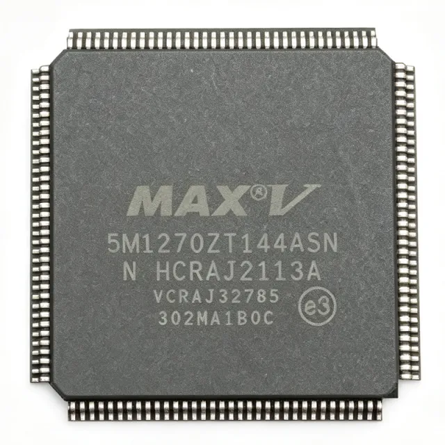
5M1270ZT144A5N - 980-Macro Cell MAX V CPLD, TQFP-144 | Intel
MPN: 5M1270ZT144A5N ✓ Active| Qty | Unit Price | Extended |
|---|---|---|
| 1 | $38.5 | $38.50 |
| 10 | $34.2 | $342.00 |
| 100 | $28.75 | $2,875.00 |
| 250 | $25.1 | $6,275.00 |
| 500 | $22.4 | $11,200.00 |
| 1,000 | $19.85 | $19,850.00 |
5M1270ZT144A5N Overview
A CPLD (Complex Programmable Logic Device) is a non-volatile programmable logic device that combines the instant-on behavior of a small PAL/GAL array with the logic density of an FPGA, typically used for glue logic, bus interfacing, power-up sequencing, and state-machine control. The MAX V family sits between discrete logic and high-density FPGAs in the programmable logic taxonomy: CPLD -> programmable logic -> logic IC -> integrated circuit -> semiconductor. Each macro cell includes a programmable AND/OR array plus a flip-flop, which the Quartus II / Quartus Prime toolset synthesizes from VHDL or Verilog.
Key features include 980 macro cells (equivalent to ~2120 logic elements), 8 Kbits of user flash memory, a MultiVolt I/O interface, an on-chip oscillator, and IEEE 1149.1 JTAG boundary-scan support. The 5N speed grade combined with the 144-pin TQFP package targets designs that need medium-density logic, abundant I/O, and hand-solderable or socketed assembly rather than fine-pitch BGA mounting. Internal pull-up resistors and bus-hold circuitry simplify board design by eliminating external termination on many signal lines.
The architecture is based on a non-volatile flash look-up table with CMOS process technology, providing instant-on capability and removing the need for an external boot PROM. The device supports in-system programmability via JTAG and is compatible with the Quartus II design software, which enables integration with both legacy schematic entry and modern HDL-based flows. AEC-Q100 qualification supports automotive deployments where the broader MAX V family is used.
Typical applications include I/O expansion and bus bridging for microcontrollers and SoCs, power-up and power-down sequencing for multi-rail systems, glue logic replacement for discrete 74-series gates, LED display driving, and protocol conversion (for example, SPI to parallel or UART to SPI). The TQFP-144 footprint also makes it suitable for educational platforms and rapid-prototyping boards where a socketed part is preferred over a BGA.
When designing with this part, place 0.1 uF and 10 uF decoupling capacitors close to every VCCINT and VCCIO pin, and observe the multi-voltage I/O bank rules so that 5 V-tolerant inputs do not exceed absolute maximum ratings. Designers migrating from legacy MAX 7000 or MAX II parts should note that MAX V delivers up to 2x higher logic density per macro cell and adds user flash, but uses the same JTAG programming chain and pinout philosophy for backward-compatible boards.
This page synthesizes verified distributor inventory, drop-in same-package alternatives drawn from the MAX V family, and practical design notes that go beyond the manufacturer datasheet table. Pricing is shown as of 2026-10-06 from DigiKey, Mouser, and Octopart.
Drop-in alternatives for 5M1270ZT144A5N — same package, pin-to-pin compatible. Different-package parts requiring PCB rework are excluded.
Variants in this series
Same-series models that are drop-in compatible with 5M1270ZT144A5N (same form factor and footprint) — differing in Operating Temperature, Package, Programming Interface, Configuration Memory, Logic Array Blocks (LABs).
Quick Comparison Tool — Select alternative parts for side-by-side comparison:
5M1270ZT144C5N
✅ Drop-In✓ In Stock
$12.45 / Unit
View Datasheet →5M1270ZT144I5N
✅ Drop-In✓ In Stock
$17.9 / Unit
View Datasheet →5M2210ZT144A5N
✅ Drop-In ⚠️ Specs Unverified📋 Reference alternative (not in catalog)
5M1270ZF256A5N
✅ Drop-In✓ In Stock
$24.1 / Unit
View Datasheet →5M1270ZT144A5N Maximum Ratings & Electrical Characteristics
| Family | MAX V |
| Device Type | CPLD (Complex Programmable Logic Device) |
| Macro Cells | 980 |
| User I/Os | 114 |
| Logic Elements | 2120 (approx.) |
| User Flash Memory | 8 Kbits |
| Maximum Operating Frequency | 201.1 MHz |
| Speed Grade | 5N |
| Core Supply Voltage | 1.8 V |
| I/O Bank Voltage Support | 1.8 V / 2.5 V / 3.3 V / 5.0 V (MultiVolt) |
| Package | TQFP-144 (T144) |
| Mounting Type | Surface Mount |
| Process Technology | Non-volatile flash CMOS |
| Programming Interface | JTAG (IEEE 1149.1) |
| Design Software | Quartus II / Quartus Prime |
| Operating Temperature | -40C to +125C (automotive) |
| Automotive Qualification | AEC-Q100 |
| RoHS Status | Compliant |
| Internal Features | Pull-up resistors, bus-hold, on-chip oscillator |
5M1270ZT144A5N tqfp-144 (t144) Pin Configuration Guide
Pin configuration for 5M1270ZT144A5N (tqfp-144 (t144) package). This digital IC includes GPIO, communication interfaces (UART, SPI, I2C), and power pins. Refer to the manufacturer datasheet for alternate pin functions and configuration options. Essential for embedded system design and PCB layout.

No detailed pinout data available for 5M1270ZT144A5N.
Refer to the datasheet for full pin configuration.
Typical Applications
5M1270ZT144A5N is suitable for 6 applications: Automotive Body Electronics and Gateway Modules, Microcontroller and SoC I/O Expansion, Power-Up and Power-Down Sequencing, Glue Logic Replacement for 74-Series Gates, Protocol Conversion and Bus Bridging, Industrial Control and Test Instrumentation.
Automotive Body Electronics and Gateway Modules
The 5M1270ZT144A5N's AEC-Q100 qualification and -40C to +125C operating range make it well suited for automotive body control modules and CAN/LIN gateway designs. With 980 macro cells and 114 user I/Os in the TQFP-144 footprint, it can host CAN/LIN message routing, lighting and seat-control glue logic, and wake-up sequencing without needing an external boot PROM. Its 8 Kbits of user flash store diagnostic counters and calibration tables that survive key-off battery disconnects, and JTAG in-system programmability supports late-stage firmware updates on the assembly line.
Recommended
Microcontroller and SoC I/O Expansion
Designers using small microcontrollers or SoCs that lack enough pins use the 5M1270ZT144A5N as an I/O expander and bus translator. The MAX V's MultiVolt I/O banks interface directly to 1.8 V, 3.3 V, and 5.0 V peripherals without level shifters, while 980 macro cells are enough to implement PWM generators, quadrature decoders, or display multiplexers. The non-volatile flash boot eliminates external boot memory and the JTAG chain allows the SoC firmware team to update CPLD logic alongside the MCU image.
Recommended
Power-Up and Power-Down Sequencing
Power-sequencing for multi-rail systems is a textbook use case for the 5M1270ZT144A5N. The CPLD's deterministic instant-on boot lets it assert enable signals in a precise order across DC-DC converters, ASICs, and FPGAs, avoiding latch-up and in-rush faults. The 980 macro cells comfortably handle 8 to 16 sequenced rails with margin for fault monitoring and watchdog logic, and the 114 user I/Os provide plenty of dedicated enable, power-good, and fault lines. JTAG lets engineers iterate the sequencing chain in-circuit without rework.
Recommended
Glue Logic Replacement for 74-Series Gates
Boards originally built with dozens of 74HC/74LVC discrete gates can be consolidated onto a single 5M1270ZT144A5N, reducing board area and BOM cost. Each macro cell replaces several discrete gates, and Quartus Prime synthesis maps legacy schematic-capture designs directly onto MAX V. The TQFP-144 footprint is hand-solderable and socketable, simplifying rework and field replacement. Designers retain JTAG visibility into internal logic nodes for debug, which is impossible with discrete gates.
Recommended
Protocol Conversion and Bus Bridging
The 5M1270ZT144A5N commonly bridges between legacy and modern buses such as SPI to parallel, UART to SPI, or I2C to GPIO. The MultiVolt I/O banks handle mixed-voltage buses without external translators, and 980 macro cells are sufficient for full-duplex state machines plus FIFO buffers. JTAG-based in-system programmability means firmware engineers can fix bridging bugs in the field without board respins, which is especially valuable for industrial and medical equipment.
Recommended
Industrial Control and Test Instrumentation
Industrial PLCs, motor controllers, and test instruments benefit from the 5M1270ZT144A5N's deterministic boot, 114 user I/Os, and wide -40C to +125C operating range. The CPLD drives front-panel LEDs and seven-segment displays, decoders quadrature encoders, and handles emergency-stop logic with deterministic latency. The TQFP-144 package is socketable for ruggedized or repairable industrial assemblies, and 8 Kbits of user flash stores calibration data and serial numbers.
Recommended
Recommended Products Summary
Engineering reference data for 5M1270ZT144A5N — comparison, design guidance, and compliance information.
Selection Guide
Comparison with Alternatives
| Parameter | This Product | 5M1270ZT144C5N | 5M1270ZT144I5N | 5M2210ZT144A5N | 5M1270ZF256A5N |
|---|---|---|---|---|---|
| Package | TQFP-144 | TQFP-144 - same | TQFP-144 - same | TQFP-144 - same | FBGA-256 - different |
| Brand | Intel (formerly Altera) | Intel - same | Intel - same | Intel - same | Intel - same |
| Macro Cells | 980 | 980 | 980 | 2210 | 980 |
| User I/Os | 114 | 114 | 114 | 114 | 212 |
| Maximum Frequency | 201.1 MHz | 201.1 MHz | 201.1 MHz | 201.1 MHz | 201.1 MHz |
| Temperature Grade | -40C to +125C (AEC-Q100) | 0C to +85C | -40C to +85C | -40C to +125C (AEC-Q100) | -40C to +125C (AEC-Q100) |
| Core Voltage | 1.8 V | 1.8 V | 1.8 V | 1.8 V | 1.8 V |
| Programming Interface | JTAG (IEEE 1149.1) | JTAG - same | JTAG - same | JTAG - same | JTAG - same |
Key Differentiators
- AEC-Q100 automotive qualification with extended temperature range (vs 5M1270ZT144C5N)
- Higher logic density than the C-grade sibling for the same footprint (vs 5M1270ZT144C5N)
- TQFP-144 footprint allows hand-soldering and socketed assembly (vs 5M1270ZF256A5N (FBGA-256))
Design Notes
Place a 0.1 uF decoupling capacitor within 5 mm of every VCCINT and VCCIO pin, and bulk 10 uF ceramic capacitors near each supply rail. The MAX V CPLD has separate core (1.8 V) and I/O bank supplies; tying all VCCIO banks to the same rail is allowed but mixing 1.8 V, 3.3 V, and 5.0 V across banks enables direct multi-voltage interfacing. Estimate inrush at ~50 mA per bank at power-up, so the upstream regulator must supply that transient without sagging.
The TQFP-144 has a 0.5 mm pitch and exposed thermal pad (EP) on most MAX V packages; flood the EP with a continuous ground copper pour and stitch it with 0.3 mm thermal vias on a 1.2 mm grid. Route all JTAG signals (TCK, TMS, TDI, TDO) as a daisy chain with 4.7 kohm pull-ups on TCK/TMS/TDI to prevent floating during programming. Keep JTAG traces short (under 100 mm) and away from switching power nodes to avoid programming errors.
Do not apply 5 V to MAX V I/O pins when VCCIO is set to 1.8 V - although the inputs are 5 V-tolerant relative to VCCIO bank voltage, absolute maximum ratings are violated if the bank itself is below the input. Also avoid driving JTAG lines while VCCINT is ramping; the recommended power-on sequence is VCCINT first, then VCCIO, to prevent latch-up. Designers migrating from MAX 7000 must update their .pof files since MAX V uses the newer JIC format for JTAG programming.
Although the 5M1270ZT144A5N is a slow CMOS device (sub-200 MHz), the TQFP-144 lead inductance (~2 nH per pin) can still cause ringing on fast edges. Add 22-33 ohm series resistors on clock inputs and high-speed outputs when driving traces longer than 50 mm. Internal pull-ups are weak (~25 kohm); for bus-hold or strong pull-up requirements, add external 10 kohm resistors.
Compliance Information
AEC-Q100 qualified per the Z suffix in the part number; RoHS and lead-free per Intel MAX V product family datasheet. Halogen-free and conflict-minerals compliance stated on Intel/Altera material declaration.





