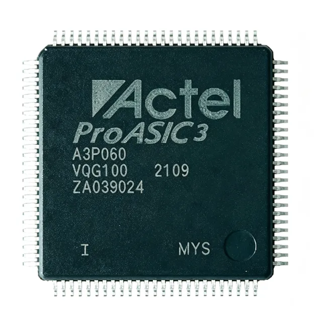
The A3P060-VQG100I is a Microchip Technology ProASIC3 flash-based field programmable gate array (FPGA) with 60,000 system gates, 700 logic elements, 71 user I/Os, and 18,432 RAM bits in a 100-pin TQFP/VQFP package. It runs from a 1.5V core, delivers up to 231 MHz system performance, and is rated for -40°C to +100°C industrial operation. Because its configuration cells are flash-based, it powers up instantly as a single chip with no external boot PROM, making it ideal for industrial automation, communications, test and measurement, medical monitoring, data acquisition, and aerospace electronics. The part is active in lifecycle status and available now on XAIPART with 99,999 units in stock, MOQ 1, priced from $9.7595 (qty 1) down to $6.95 (qty 1,000) as of 2026-09-02.
What Are the Quick Answers About the A3P060-VQG100I?
The A3P060-VQG100I sits above simple programmable logic devices and below complex SoC FPGAs. Its 130nm flash process enables non-volatile configuration, secure programming with FlashLock, and low total cost of ownership. Unlike SRAM-based FPGAs, it needs no external configuration memory, which reduces board area, BOM cost, and power-up failure risk.
Key verified specifications at a glance:
| Parameter | Value |
|---|---|
| Manufacturer | Microchip Technology |
| Family / Series | ProASIC3 |
| System Gates | 60K |
| Logic Elements | 700 |
| User I/O | 71 |
| RAM Bits | 18,432 |
| Max System Performance | 231 MHz |
| Process | 130 nm flash |
| Core Voltage | 1.5 V |
| Package | 100-TQFP / VQFP-100, surface mount, tray |
| Temperature Range | -40°C to +100°C (industrial) |
| Configuration | Flash-based, reprogrammable |
| Lifecycle | Active |
On XAIPART, the base price is $6.95 at 1,000 units as of 2026-09-02, with 99,999 units in stock and MOQ of 1. Speed grade suffix, supported I/O standards, PLL count, dedicated clock inputs, and RoHS status are not listed in the verified database: [DATA_NEEDED: Speed grade suffix], [DATA_NEEDED: Supported I/O standards], [DATA_NEEDED: Number of PLLs], [DATA_NEEDED: Number of clock inputs], [DATA_NEEDED: RoHS status from datasheet/package marking].
How Do You Select and Design In the A3P060-VQG100I?
Selection starts with capacity matching. With 700 logic elements and 60K gates, the A3P060-VQG100I handles control logic, bus interfaces, state machines, FIFO control, and moderate DSP tasks. Its 18,432 RAM bits buffer short data segments between acquisition front ends and a host processor. If your design needs more logic, the same ProASIC3 architecture scales to higher-density parts in the family.
Power and thermal design matter. The 1.5V core combined with the 130nm process keeps dynamic power low, which matters inside dense enclosures and battery-adjacent systems. Pay close attention to core voltage decoupling, I/O bank voltage requirements, and thermal management of the TQFP-100 package. Exact I/O bank voltage options are not in the verified data: [DATA_NEEDED: Supported I/O standards].
Configuration and security: because the device is flash-based, configure FlashLock security and JTAG access carefully to protect intellectual property. Instant-on startup eliminates host-driven configuration, which is critical for instruments that must be ready immediately at power-up.
Environmental fit: choose the I-suffix industrial part when the end product must operate from -40°C to +100°C — outdoor equipment, factory floors, remote radio units, and avionics. The commercial-grade A3P060-VQG100 (0°C to +70°C) suffices for indoor consumer or office equipment and is pin-compatible.
Sourcing: the verified tiered pricing on XAIPART as of 2026-09-02 is $9.7595 at qty ≥1, $8.95 at ≥10, $8.05 at ≥100, $7.45 at ≥500, and $6.95 at ≥1,000. Microchip Direct has historically estimated about 28 weeks of factory lead time for additional units, so plan volume purchases ahead and check distributor stock at order time.
What Are the Best Drop-In Alternatives to the A3P060-VQG100I?
All verified drop-in alternatives come from the same ProASIC3 family in the same 100-pin VQFP footprint. No cross-brand pin-compatible replacement was found in the verified data.
| Parameter | A3P060-VQG100I | A3P060-VQG100 | A3P060-1VQG100I | A3P060-1VQ100I |
|---|---|---|---|---|
| Package | 100-TQFP / VQFP-100 | 100-TQFP / VQFP-100 | VQG100 (100-pin) | 100-pin VQFP family |
| Temperature Range | -40°C to +100°C | 0°C to +70°C | Industrial | Industrial |
| Speed Grade | Standard | Standard | -1 | -1 |
| Architecture / Gates | ProASIC3, 60K | ProASIC3, 60K | ProASIC3, 60K | ProASIC3, 60K |
| Drop-in Replacement | — | Yes (if commercial temp acceptable) | Yes (higher timing margin) | Yes |
Choose A3P060-VQG100 when your thermal environment allows 0°C to +70°C. Choose A3P060-1VQG100I when your design needs the -1 speed grade for stricter timing closure. A3P060-2VQG100I and A3P060-1VQ100T are also same-family options mentioned in verified FAQ data. Comparative pricing for these alternatives is not in the verified database: [DATA_NEEDED: pricing for A3P060-VQG100, A3P060-1VQG100I, A3P060-1VQ100I].
What Is the Market Position and Supply Situation for the A3P060-VQG100I?
Lifecycle status is active per the verified database. XAIPART shows 99,999 units in stock with MOQ 1 as of 2026-09-02. Distributor-level data from the FAQ records: LCSC listed 15 units in stock, and Microchip Direct listed approximately 4,310 units with an estimated factory lead time of about 28 weeks for additional units. Stock levels change frequently, so confirm availability before ordering. Lifecycle forecast data (e.g., discontinuation or end-of-life notices) is not present in the verified data: [DATA_NEEDED: lifecycle forecast / EOL notice].
What Trends Should Buyers Watch for This FPGA?
Three factors anchored to verified specs: First, lead time — the ~28-week factory lead time estimate means buyers should buffer inventory; XAIPART's 99,999-unit stock at MOQ 1 mitigates near-term risk. Second, temperature-grade consolidation — designing on the -40°C to +100°C industrial grade future-proofs designs against harsh-environment deployments without a PCB respin, since the I and non-I parts are pin-compatible. Third, single-chip flash architecture — as systems demand instant-on, secure (FlashLock), and low-power logic (1.5V core, 130nm process), flash FPGAs like the ProASIC3 remain relevant where SRAM FPGAs need external boot memory. Verify current pricing against the tiers above as of 2026-09-02 before finalizing your BOM.
How Does the Design Math Work in a Real Application?
Consider a multi-channel data acquisition module. The verified 71 user I/Os can be partitioned across parallel ADC/DAC interfaces, an external memory bus, and a trigger distribution network, while 18,432 RAM bits buffer data between the acquisition front end and a host processor. The 700 logic elements implement FIFO control and channel averaging, and the 231 MHz maximum system performance sets the upper bound on pipeline clocking. Industrial -40°C to +100°C rating allows deployment in remote, outdoor instrumentation. Exact I/O standards and PLL resources needed for detailed timing closure are not in the verified data: [DATA_NEEDED: Supported I/O standards], [DATA_NEEDED: Number of PLLs].
Comments
Be the first to comment.
🔐 Please sign in to post a comment.
Don't have an account? Sign up