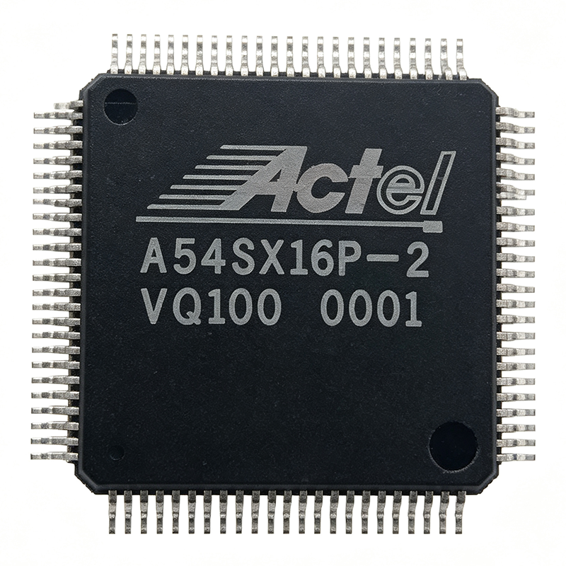
What Is the A54SX16-VQ100 and Why Do Engineers Still Specify It?
The A54SX16-VQ100 is a Microsemi (Actel, now Microchip) SX-family antifuse FPGA delivering 16,000 system gates and 924 logic cells with a maximum system frequency of 240 MHz and 81 user I/O in a 100-pin TQFP (VQFP, 14x14 mm) surface-mount package. It operates from dual supply rails of 3.0V–3.6V and 4.75V–5.25V, is fabricated on a 0.35 um CMOS process, and configures instantly at power-up because its antifuse interconnect is hard-wired in silicon — no external boot PROM or configuration sequence. On XAIPART, the part is listed as active with stock of 99,999 units, MOQ 1, and quote-based pricing as of 2026-09-12; the base price field shows $0, meaning buyers should request a quotation for current distributor pricing.
Unlike SRAM FPGAs, the SX family is one-time programmable: interconnects are programmed once at programming time, producing non-volatile, low-power configuration with inherent protection against configuration readback. The sea-of-modules architecture combining C-cells (combinational) and S-cells (sequential) yields gate utilization and speed close to mask ASICs, with deterministic sub-nanosecond pin-to-pin delays. These traits make the A54SX16-VQ100 a continuing choice for industrial control, communications glue logic, avionics and defense subsystems, ASIC prototyping, and instant-on bridge and bus interface logic.
How Do You Select and Design In the A54SX16-VQ100?
Designing in the A54SX16-VQ100 starts with capacity and interface budgeting. The device provides 16,000 system gates and 924 logic cells of flip-flop-rich logic — enough to integrate glue logic, bus bridging, state machines, counters, and protocol bridging that would otherwise occupy multiple PAL/GAL devices. With 81 user I/O, it accommodates 16/32-bit parallel data paths, address decoding, and handshaking. The dual-rail supply architecture (3.0V–3.6V core/IO rail and 4.75V–5.25V rail) lets the device interface directly with legacy 5V logic while running a 3.3V core.
Follow this selection and design-in sequence:
Step 1 — Confirm capacity headroom. Map your RTL into the SX16 library and check utilization. The sea-of-modules fabric maps synchronous ASIC-style code efficiently, but antifuse devices cannot be resized in the field, so reserve margin for engineering changes. If the design fits comfortably below 8,000 gates with 20–30% headroom, the lower-cost A54SX08-VQG100 in the same footprint is an option; if it exceeds SX16 capacity, move up the family to SX32 parts in larger packages while reusing much of the code base.
Step 2 — Choose the correct speed and temperature grade. The commercial-grade A54SX16-VQ100 is the standard variant. For industrial temperature ranges, Microsemi offered the A54SX16-VQ100I industrial variant and industrial speed-grade suffixes such as SX16P VQG100I parts. Verify the exact temperature grade on the device marking before using the part outside 0°C to +70°C conditions, and order the 'I'-suffixed ordering code for a guaranteed industrial specification. [DATA_NEEDED: operating temperature range of the standard commercial part]
Step 3 — Power design. Plan dual rails: one within 3.0V–3.6V and one within 4.75V–5.25V. Because antifuse configuration is non-volatile, the device is functional at power-up with no in-rush associated with bitstream loading, simplifying brownout behavior — there is no risk of a corrupted bitstream leaving machinery in an undefined state after a power dip, a common SRAM FPGA failure mode.
Step 4 — PCB footprint and pinout. Use the 100-pin VQFP footprint (14x14 mm body). The complete pin-for-pin table for the 100-pin VQFP, including the 81 user I/O, dedicated VDD, GND, and programming pins arranged around the quad flat package, is in the packaging section of the '54SX Family FPGAs' datasheet published by Microchip Technology.
Step 5 — Validate thoroughly before programming. Antifuse FPGAs are one-time programmable — any logic change requires a new device. Complete full simulation, timing closure, and post-layout static timing analysis in the Actel/Microchip tools before committing to production programming. Because the SX architecture delivers deterministic, ASIC-like timing, post-layout static timing analysis gives reliable frequency verification up to the 240 MHz maximum system frequency; actual achievable frequency depends on the speed grade ordered, routing density, and I/O timing requirements.
Step 6 — Plan spares. Reserve spare I/O in your pin assignment. Since reprogramming is impossible, a pin-mapping change for a board revision would otherwise force a new programmed device set.
What Are the Best Drop-In Alternatives to the A54SX16-VQ100?
Drop-in replacements come from the same Actel SX antifuse family in the identical 100-pin VQFP footprint: A54SX16P-VQG100, A54SX16P-1VQG100, A54SX16P-2VQG100, A54SX16P-VQG100I, and A54SX08-VQG100. All are pin-compatible with the original, so no PCB rework is needed. No cross-brand pin-compatible drop-in exists for Actel antifuse FPGAs — functional replacements from other FPGA vendors require PCB and code redesign. Note that because these are one-time-programmable devices, any substitution requires recompiling the design with the target device's library and reprogramming the part; verify timing closure after substitution since the SX16P variants carry different timing specifications.
| Parameter | A54SX16-VQ100 (verified) | A54SX16P-VQG100 | A54SX08-VQG100 |
|---|---|---|---|
| Family | SX (Actel antifuse FPGA) | SX16P (same family, 'plus' variant) | SX (same family) |
| System Gates | 16,000 | [DATA_NEEDED: system gates for A54SX16P-VQG100] | 8,000 (per FAQ: lower gate count) |
| Logic Cells | 924 | [DATA_NEEDED: logic cells for A54SX16P-VQG100] | [DATA_NEEDED: logic cells for A54SX08-VQG100] |
| Max System Frequency | 240 MHz | Higher speed grades / enhanced performance (per FAQ) | [DATA_NEEDED: max frequency] |
| Package | 100-TQFP (VQFP, 14x14 mm) | 100-pin VQFP, pin-compatible footprint | 100-pin VQFP, same footprint |
| Programming | Antifuse (one-time programmable) | Antifuse (one-time programmable) | Antifuse (one-time programmable) |
| Best Use | Baseline 16K-gate designs | Performance upgrade, same footprint | Cost reduction when 8K gates suffice |
Which variant should you choose? Use the A54SX16P-VQG100 when you need higher performance in the identical footprint — designs compiled for the SX16 generally port to the SX16P with recompilation, but verify timing closure because the two are distinct orderable devices with different timing specifications. Use the A54SX08-VQG100 to reduce cost when the implemented design fits below SX08 capacity with at least 20–30% headroom. Note also that A54SX16-VQ100 and A54SX16-VQG100 are essentially the same device differing only in packaging code: the VQG100 is the green (RoHS-era) packaging variant containing the identical 16K-gate SX16 die.
Where Is the A54SX16-VQ100 Used in Real Systems?
The verified application profile for this device spans six scenarios, each exploiting the antifuse fabric's instant-on, deterministic, and secure configuration:
Industrial control and automation. The dual 3.3V/5V supply architecture (3.0V–3.6V and 4.75V–5.25V rails) interfaces directly with legacy 5V industrial logic while using a 3.3V core. Instant-on antifuse configuration means PLC glue logic, motor-drive interface sequencing, and sensor aggregation across 81 user I/O are functional the moment power is applied, with no risk of a corrupted bitstream after a brownout.
Communications and networking interface logic. In telecom and datacom line cards, the device serves as high-speed glue logic, protocol bridging, and backplane interface control. Deterministic, ASIC-like timing with system performance up to 240 MHz suits time-critical framing, multiplexing, and status monitoring, while the antifuse fabric adds no configuration-readback security exposure — valuable for carrier equipment. The 14x14 mm 100-TQFP keeps board area compact in 19-inch rack card designs.
Avionics and defense subsystems. One-time-programmed configuration is immune to single-event configuration upset and cannot be extracted or modified in the field. The 16,000 gates and 924 cells host interfaces, arbiters, and built-in-test logic; instant-on operation ensures the subsystem is live before system-level health checks complete. For new designs needing guaranteed temperature grades, the industrial-qualified A54SX16P-VQG100I in the same footprint provides an upgrade path without PCB change.
ASIC prototyping and emulation. The 924-cell sea-of-modules fabric with flip-flop-rich S-cells maps synchronous ASIC-style RTL efficiently, achieving timing up to 240 MHz. Permanently programmed prototype builds serve as true, non-modifiable golden references for pre-silicon system validation; designs needing more capacity move to SX32 parts while reusing code.
Bridge and bus interface logic. The bridge is active before a host CPU finishes reset, avoiding boot-order dependencies. The 5V-compatible supply option (4.75V–5.25V) lets it sit directly on legacy 5V buses, and deterministic pin-to-pin delays simplify meeting bus setup and hold budgets.
Test and measurement equipment. Low skew and deterministic delays let trigger chains meet tight channel-to-channel alignment; 16K gates integrate counter arrays, comparators, and state machines. One-time programmability guarantees identical behavior across calibration cycles — an auditable advantage for ISO-controlled production test — and instant-on configuration reduces instrument startup time versus SRAM FPGA platforms.
What Is the Market Position and Supply Situation for the A54SX16-VQ100?
The A54SX16-VQ100 is listed as active in the XAIPART database, but it is a mature Actel-era (Microsemi/Microchip) device. Availability comes primarily from distributor stock and excess inventory rather than new production: secondary-market distributors report Heisener with 6,688 pieces in stock (lead time to be confirmed), and DigiKey shows the part under its Microchip listing shipping from available inventory. Octopart lists the part across 9 distributors, with prices varying significantly by stock age and quantity. Pricing on XAIPART is quote-based because this legacy antifuse FPGA has variable distributor stock; the database base price shows $0 as of 2026-09-12, and buyers above available stock should expect extended sourcing times typical of legacy Actel-era components. Request a quote from XAIPART for current committed delivery.
What Should Buyers Watch: Trends and Outlook for the A54SX16-VQ100?
Anchor your buying decisions to these verified facts. First, the device's 240 MHz maximum system frequency, 16,000 gates, and 924 logic cells are fixed silicon characteristics — they will not improve, so performance-driven new designs should evaluate the SX16P variants (A54SX16P-VQG100 and its -1/-2 speed grades) in the same footprint, recompiling and verifying timing closure. Second, supply depends on distributor stock: with Heisener reporting 6,688 pieces and availability drawn from excess inventory rather than fresh production, verify real-time stock before committing to a production schedule and consider lifetime-buy quantities for long-lived industrial, avionics, and test-equipment programs. Third, temperature-grade selection matters: the commercial A54SX16-VQ100 is specified for 0°C to +70°C conditions, so order 'I'-suffixed codes (A54SX16-VQ100I or A54SX16P-VQG100I) for guaranteed industrial specification. Fourth, because antifuse parts are one-time programmable, budget for spares — any logic change consumes new devices. Finally, the same-footprint green packaging variant A54SX16-VQG100 is cross-referenced as equivalent, which widens your qualified sourcing pool without PCB or design change.
Comments
Be the first to comment.
🔐 Please sign in to post a comment.
Don't have an account? Sign up