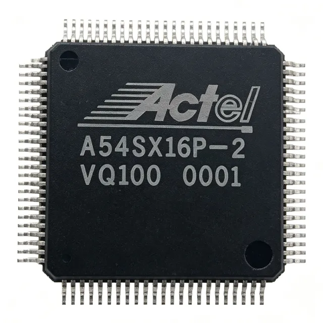
A54SX16-VQ100 - SX FPGA 16K Gates 100-TQFP | Microsemi
MPN: A54SX16-VQ100 ✓ Active| Qty | Unit Price | Extended |
|---|---|---|
| 1 | $0 | $0.00 |
| 10 | $0 | $0.00 |
| 100 | $0 | $0.00 |
| 500 | $0 | $0.00 |
| 1,000 | $0 | $0.00 |
A54SX16-VQ100 Overview
An FPGA (Field Programmable Gate Array) is a semiconductor device containing a fabric of configurable logic blocks and programmable interconnects that the designer programs after manufacturing. Within the product hierarchy, the A54SX16 sits under FPGA -> programmable logic device -> digital integrated circuit. The SX family is unique among FPGAs because it uses Actel's antifuse technology: interconnects are one-time programmable at programming time, giving non-volatile, radiation-tolerant, low-power configuration without an external configuration PROM or boot sequence.
Key differentiating features include the sea-of-modules architecture that yields gate utilization and speed close to mask ASICs, deterministic sub-nanosecond pin-to-pin delays, and instant-on operation at power-up because the configuration is hard-wired in silicon. The 0.35 um antifuse process also provides inherent protection against configuration readback, a security advantage over SRAM FPGAs.
Architecturally, the SX family combines C-cells (combinational) and S-cells (sequential) in clusters, with the A54SX16 providing 924 cells of high-speed, flip-flop-rich logic. The device is programmed once using Actel/Microchip programming tools, after which the design is fixed for life - ideal for production systems where configuration integrity matters.
Typical applications include industrial control, communications and networking glue logic, avionics and military subsystems, and ASIC prototyping where 16K gates suffice. Instant-on behavior also suits bridge and interface logic on boards that cannot wait for configuration.
Design consideration: antifuse FPGAs are one-time programmable - any logic change requires a new device, so reserve spare I/O and validate the design thoroughly in simulation before committing to production programming.
This page synthesizes verified distributor data, drop-in alternatives from the same SX family, and practical design notes not found in the manufacturer datasheet.
Drop-in alternatives for A54SX16-VQ100 — same package, pin-to-pin compatible. Different-package parts requiring PCB rework are excluded.
Variants in this series
Same-series models that are drop-in compatible with A54SX16-VQ100 (same form factor and footprint) — differing in System Gates, Process Technology, Logic Cells, Architecture, Family.
Quick Comparison Tool — Select alternative parts for side-by-side comparison:
A54SX16P-VQG100
✓ In Stock
$47.6 / Unit
View Datasheet →A54SX16P-1VQG100
✓ In Stock
$25.1 / Unit
View Datasheet →A54SX16P-2VQG100
✓ In Stock
$30.1 / Unit
View Datasheet →A54SX16P-VQG100I
✓ In Stock
Contact for price
View Datasheet →A54SX08-VQG100
✓ In Stock
$32.1 / Unit
View Datasheet →A54SX16-VQ100 Maximum Ratings & Electrical Characteristics
| Family | SX (Actel antifuse FPGA) |
| System Gates | 16000 gates |
| Logic Cells | 924 cells |
| Maximum System Frequency | 240 MHz |
| Process Technology | 0.35 um CMOS |
| Supply Voltage (Core/IO) | 3 V to 3.6 V and 4.75 V to 5.25 V |
| Number of I/O | 81 |
| Package | 100-TQFP (VQFP, 14x14 mm) |
| Programming Technology | Antifuse (one-time programmable) |
| Mounting Type | Surface Mount |
| Configuration Type | Non-volatile, instant-on |
A54SX16-VQ100 100-tqfp (vqfp, 14x14 mm) Pin Configuration Guide
Pin configuration for A54SX16-VQ100 (100-tqfp (vqfp, 14x14 mm) package). This digital IC includes GPIO, communication interfaces (UART, SPI, I2C), and power pins. Refer to the manufacturer datasheet for alternate pin functions and configuration options. Essential for embedded system design and PCB layout.

No detailed pinout data available for A54SX16-VQ100.
Refer to the datasheet for full pin configuration.
Typical Applications
A54SX16-VQ100 is suitable for 6 applications: Industrial Control and Automation, Communications and Networking Interface Logic, Avionics and Defense Subsystems, ASIC Prototyping and Emulation, Bridge and Bus Interface Logic, Test and Measurement Equipment.
Industrial Control and Automation
The A54SX16-VQ100's 5V-tolerant I/O and instant-on antifuse configuration make it well suited to industrial control boards that must be functional the moment power is applied. With 81 user I/O it can integrate PLC glue logic, motor-drive interface sequencing, and sensor aggregation in one 16K-gate device running at up to 240 MHz. Because the configuration is hard-wired in silicon, there is no risk of a corrupted bitstream leaving machinery in an undefined state after a brownout, a common failure mode of SRAM FPGAs. The dual 3.3V/5V supply architecture also lets it interface directly with legacy 5V industrial logic while using a 3.3V core.
Recommended
Communications and Networking Interface Logic
In telecom and datacom line cards, the A54SX16-VQ100 serves as high-speed glue logic, protocol bridging, and backplane interface control. The SX family's deterministic, ASIC-like timing - with system performance up to 240 MHz on 0.35 um technology - suits time-critical framing, multiplexing, and status monitoring paths where SRAM FPGA reconfiguration delays are unacceptable. Its antifuse fabric adds no configuration-readback security exposure, valuable for carrier equipment. The 100-pin TQFP with 81 I/O provides enough pin count for parallel data buses and control signals while the 14x14 mm body keeps board area compact in 19-inch rack card designs.
Recommended
Avionics and Defense Subsystems
Actel antifuse FPGAs are a longstanding choice in avionics and defense electronics because the one-time-programmed configuration is immune to single-event configuration upset and cannot be extracted or modified in the field. The A54SX16-VQ100 provides 16,000 gates and 924 cells for interfaces, arbiters, and built-in-test logic in mission computers and sensor heads. Instant-on operation ensures the subsystem is live before system-level health checks complete. For new designs requiring guaranteed temperature and screening grades, the industrial-qualified A54SX16P-VQG100I in the same footprint provides an upgrade path without PCB change.
Recommended
ASIC Prototyping and Emulation
Before committing an ASIC mask set, designers historically mapped RTL into Actel SX FPGAs to validate logic behavior in silicon. The A54SX16-VQ100's 924-cell sea-of-modules fabric with dedicated flip-flop-rich S-cells maps synchronous ASIC-style code efficiently and yields timing up to 240 MHz, faster than typical SRAM FPGA prototypes of its era. Because antifuse programming permanently fixes the design, prototype builds on this device represent a true, non-modifiable golden reference for pre-silicon system validation. Designs needing more capacity move up the family to SX32 parts in larger packages while reusing much of the code base.
Recommended
Bridge and Bus Interface Logic
The A54SX16-VQ100 fits naturally as bus bridge logic between microprocessors, memory, and peripherals on boards that power up instantly. Its non-volatile antifuse configuration means the bridge is active before a host CPU finishes reset, avoiding the boot-order dependencies that SRAM FPGAs impose. The 5V-compatible supply option (4.75V-5.25V) lets the device sit directly on legacy 5V buses, while 81 I/O accommodate 16/32-bit data paths, address decoding, and handshaking. Deterministic pin-to-pin delays simplify meeting bus setup and hold budgets documented in the host controller datasheets.
Recommended
Test and Measurement Equipment
Bench and automated test instruments benefit from the A54SX16-VQ100 as timing, trigger, and scan-control logic. The SX architecture's low skew and deterministic delays let trigger chains meet tight channel-to-channel timing alignment, while 16K gates integrate counter arrays, comparators, and state machines that would otherwise need multiple PAL/GAL devices. One-time programmability guarantees the test station behaves identically across calibration cycles - an auditable advantage for ISO-controlled production test. Instant-on configuration also reduces instrument startup time compared to SRAM FPGA platforms that must load bitstreams.
Recommended
Recommended Products Summary
Engineering reference data for A54SX16-VQ100 — comparison, design guidance, and compliance information.
Selection Guide
Comparison with Alternatives
| Parameter | This Product | A54SX16P-VQG100 | A54SX16P-1VQG100 | A54SX16P-2VQG100 | A54SX16P-VQG100I | A54SX08-VQG100 |
|---|---|---|---|---|---|---|
| Package | 100-TQFP (VQFP, 14x14 mm) | 100-TQFP (VQFP) - same | 100-TQFP (VQFP) - same | 100-TQFP (VQFP) - same | 100-TQFP (VQFP) - same | 100-TQFP (VQFP) - same |
| Brand | Microsemi (Actel) | Microsemi (Actel) | Microsemi (Actel) | Microsemi (Actel) | Microsemi (Actel) | Microsemi (Actel) |
| System Gates | 16000 | 16000 | 16000 | 16000 | 16000 | 8000 |
| User I/O | 81 | 81 | 81 | 81 | 81 | 81 |
| Temperature Grade | Commercial | Commercial | Commercial | Commercial | Industrial | Commercial |
| Programming Technology | Antifuse (OTP) | Antifuse (OTP) | Antifuse (OTP) | Antifuse (OTP) | Antifuse (OTP) | Antifuse (OTP) |
Key Differentiators
- Double the logic capacity of the smaller sibling (vs A54SX08-VQG100)
- Higher performance SX16P upgrade path (vs A54SX16P-2VQG100)
- Cost advantage over industrial-grade variant (vs A54SX16P-VQG100I)
Design Notes
Antifuse devices are one-time programmable: once the A54SX16-VQ100 is programmed, its configuration cannot be altered or erased. Prototype thoroughly in the Actel/Microchip (Libero) simulation and layout flow, verify timing with post-layout static timing analysis, and reserve 15-20% spare gates and I/O for late engineering changes before committing production units. A logic bug discovered after programming requires scrapping the device.
The device supports dual supply ranges of 3.0V-3.6V and 4.75V-5.25V per the verified data. Confirm which rail powers I/O banks versus core on your board revision, and sequence supplies per the SX family datasheet power-up specification to avoid latch-up during hot insertion. Antifuse FPGAs draw negligible configuration current compared to SRAM FPGAs at power-up, simplifying inrush design on 5V backplane systems.
For the 100-TQFP 14x14 mm package, use a standard 0.5 mm pitch QFP-100 footprint and place 0.1 uF decoupling capacitors at all VDD pins within 3 mm of the package, one per pair of supply pins. Route high-speed I/O (up to 240 MHz system capability) with controlled impedance and keep stub lengths short. Follow the packaging section of the 54SX Family FPGAs datasheet for exact pin assignments when generating the footprint.
Compliance Information
Compliance data not present in verified web data. The related green packaging variant A54SX16-VQG100 is generally the RoHS-oriented ordering code; confirm RoHS status with Microchip for the specific lot before procurement.





