Quick Answers
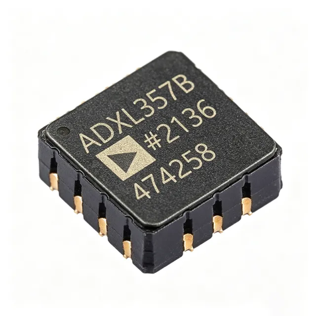
The ADXL357BEZ is a low noise, low drift, 3-axis MEMS accelerometer from Analog Devices with selectable measurement ranges of ±10g, ±20g, and ±40g. It provides digital output over SPI or I2C, runs from 2.25 V to 3.6 V, draws only 200 µA at 3.3 V, and is available now with 99,999 units in stock and a 1-piece MOQ as of 2026-08-25. The device achieves 80 µg/√Hz noise density, <0.75 mg 0 g offset drift, 1 Hz to 1 kHz bandwidth, and is housed in a 14-terminal CLCC (6x6 mm) package. It also integrates a 32-level FIFO and temperature sensor, making it a strong choice for industrial vibration monitoring, IMUs, structural health monitoring, robotics, seismic sensing, and aerospace navigation.
Pricing as of 2026-08-25: $150.00 at 1 piece, $108.33 at 10 pieces, $95.83 at 100 pieces, $91.67 at 500 pieces, and $87.50 at 1000 pieces. View the ADXL357BEZ product page.
Key verified specifications
| Parameter | Value |
|---|---|
| Measurement Range | ±10g, ±20g, ±40g (selectable) |
| Interface | SPI, I2C |
| Bandwidth | 1 Hz to 1 kHz |
| Noise Density | 80 µg/√Hz |
| 0 g Offset Drift | <0.75 mg over temperature |
| Supply Voltage | 2.25 V to 3.6 V |
| Current Consumption | 200 µA at 3.3 V |
| Package | 14-CLCC (6x6 mm) |
| Operating Temperature | -40°C to +125°C |
| FIFO | 32-level |
| Temperature Sensor | Integrated |
| RoHS | Compliant |
Technical Guide: How to Select, Design In, and Use the ADXL357BEZ
The ADXL357BEZ is a digital-output, low noise accelerometer that combines a capacitive MEMS sensing element with a high-resolution sigma-delta ADC. The device is factory-calibrated for sensitivity and offset, which reduces the need for user calibration. Three selectable g-ranges, two digital interfaces, and a 32-level FIFO make it flexible for a wide range of motion and vibration sensing applications.
Selecting the measurement range
The measurement range is selected through the digital interface. Choose ±10g when acceleration amplitudes are expected to stay low and you want the highest available resolution, ±20g for general machine vibration, and ±40g for shock-loaded or high-dynamic systems. The range setting directly affects full-scale output, so verify your expected peak acceleration before committing to a configuration.
Power supply and decoupling
The ADXL357BEZ operates from a 2.25 V to 3.6 V supply. Place a 0.1 µF capacitor close to the VDD pin and a 1 µF capacitor on the VDD I/O pin. Because the VDD I/O pin sets the digital interface voltage independently, you can connect the sensor to a 1.8 V, 2.5 V, or 3.3 V logic bus without external level shifters. A solid ground plane under the device minimizes noise coupling and improves measurement repeatability.
Connecting SPI or I2C
Use the following pins for digital communication: Pin 3 SCLK/SCL carries the SPI clock or I2C clock; Pin 4 SDI/SDA carries SPI data in or I2C data; Pin 5 SDO/ADR0 carries SPI data out or the I2C address bit; and Pin 6 CS is the chip-select input. For I2C operation, the ADR0 bit selects the device address. In SPI mode, the host controls CS and reads data from SDO. The separate VDD I/O pin lets you set the logic threshold to match the host bus voltage.
Using the FIFO and interrupts
The 32-level FIFO stores acceleration samples to reduce host processor loading. Configure INT1 (Pin 8) or INT2 (Pin 9) for data-ready, FIFO watermark, or activity/inactivity events. In a high-bandwidth vibration application, the FIFO lets a low-power MCU sleep longer and wake only when a burst of data is ready. This approach reduces average power consumption and simplifies real-time scheduling.
Noise floor and resolution
With a noise density of 80 µg/√Hz and a 1 kHz maximum bandwidth, the theoretical RMS noise floor is approximately 2.53 mg. For a typical industrial vibration-monitoring node, this sensitivity allows detection of small changes in machine health before they become critical. The low 0 g offset drift of <0.75 mg over temperature also helps maintain accurate static tilt measurements over time.
PCB layout and package
The 14-terminal CLCC package measures 6x6 mm and is designed for surface-mount assembly. Keep the decoupling capacitors as close as possible to VDD and VDD I/O, use short traces to the host MCU, and avoid routing high-speed digital lines under the sensor. The operating temperature range of -40°C to +125°C supports deployment in outdoor enclosures with wide thermal swings.
Example design: battery-powered vibration node
As a concrete design exercise, assume the host MCU uses a 3.3 V I/O bus and the sensor monitors machine vibration up to 1 kHz. Configure the ADXL357BEZ in SPI mode at ±10g range. Connect VDD to 3.3 V, place a 0.1 µF capacitor next to VDD and a 1 µF capacitor on VDD I/O. Connect SCLK to SPI clock, SDI to MOSI, SDO to MISO, and CS to a GPIO. Enable the FIFO interrupt on INT1 and set the watermark threshold to 32. The sensor will buffer 32 samples before asserting INT1, allowing the MCU to sleep until a burst is ready. Power consumption of the accelerometer is 200 µA at 3.3 V, or 0.66 mW. A 1000 mAh CR2032-class battery would theoretically power only the accelerometer for 5000 hours (1000 mAh / 0.2 mA); real designs must include MCU and radio current. The RMS noise due to the accelerometer alone at 1 kHz bandwidth is around 2.53 mg, which helps detect early bearing wear in rotating machinery.
For more design examples, see the motion sensor category.
Alternatives & Comparison: Drop-In Replacements for ADXL357BEZ
When a program needs a second source or a different output type, the ADXL357 family offers several alternatives. The ADXL357BCPZ shares the same CLCC package footprint, making it a likely drop-in for existing layouts, although its temperature grade or calibration may differ. The ADXL356BEZ is an analog output version with the same package and pinout, which can simplify direct connection to an ADC front end. The ADXL356B is an analog part that supports 10g and 20g ranges. The ADXL357B is a digital-output part with similar specifications.
| Alternative | Relationship | Verified data |
|---|---|---|
| ADXL357BCPZ | Same package variant | Same package as ADXL357BEZ; possibly different temperature grade or calibration |
| ADXL356BEZ | Analog output version | Analog output; same package and pinout as ADXL357BEZ |
| ADXL356B | Analog output alternative | Analog output; supports 10g and 20g ranges |
| ADXL357B | Digital output alternative | Digital output; similar specifications |
The verified data does not include noise, drift, supply current, or full-scale specifications for these alternatives. Before changing a BOM, obtain the target datasheet and verify electrical compatibility, timing, and temperature grade. Check live ADXL357BEZ inventory and pricing while you evaluate.
Industry Insight: Market Position, Lifecycle, and Supply
Analog Devices maintains the ADXL357BEZ as an active lifecycle part. The XAIPART database shows 99,999 units in stock with a 1-piece MOQ, indicating strong availability for prototype and production orders. The part is housed in a 14-terminal CLCC package and is RoHS-compliant. Given the active lifecycle status, buyers should not be concerned about imminent end-of-life actions. High inventory levels also mean reduced risk of allocation-driven price volatility in the near term.
Pricing tiers in the XAIPART database as of 2026-08-25 show a clear volume incentive: from $150.00 at one piece down to $87.50 at 1000 pieces. This pricing structure supports both low-volume engineering builds and higher-volume production runs.
Trends & Outlook: What Buyers Should Watch
The verified specifications of the ADXL357BEZ track several important market trends in industrial sensing and IoT.
- Low power for battery-operated nodes: At 200 µA from a 3.3 V supply, the ADXL357BEZ can extend duty cycle for wireless condition monitoring and remote seismic stations.
- Low noise for precision measurement: The 80 µg/√Hz noise density and <0.75 mg offset drift address applications that need millig-level repeatability.
- Configurable range for platform reuse: ±10g, ±20g, and ±40g ranges allow the same IP to support varied mechanical environments.
- Digital integration: SPI/I2C output with a 32-level FIFO reduces MCU overhead and design-in time.
- Temperature robustness: The -40°C to +125°C range fits outdoor, industrial, and aerospace installations.
Buyers should watch for wider adoption of low-noise MEMS accelerometers in predictive maintenance and IMU products. The active lifecycle status, RoHS compliance, and high stock count make the ADXL357BEZ a safe baseline component. For future designs, evaluating the ADXL357 family variants is advisable, but the verified supply and performance data here provide a strong foundation for current decisions.
For more technical and procurement insight, visit the XAIPART blog.
Comments
Be the first to comment.
🔐 Please sign in to post a comment.
Don't have an account? Sign up