The CDCE6214TWRGERQ1 from Texas Instruments is an automotive-grade, ultra-low power clock generator that integrates one fractional-N PLL, two clock inputs, four differential outputs, and an internal EEPROM with two pages in a compact 24-pin VQFN (4mm x 4mm) package. It supports PCIe Gen 1-5, delivers output frequencies up to 350 MHz from a single 3.3V supply, and communicates via an I2C-compatible interface up to 400 kHz. The device is AEC-Q100 qualified and rated for -40C to +125C operation, making it well suited for ADAS, automotive infotainment, industrial automation, networking, test and measurement, and data center equipment. The part is currently active in lifecycle status and available on XAIPART with 99,999 units in stock, MOQ 1, and pricing starting at $4.50 for single units down to $2.88 at 1,000 units as of 2026-09-04.
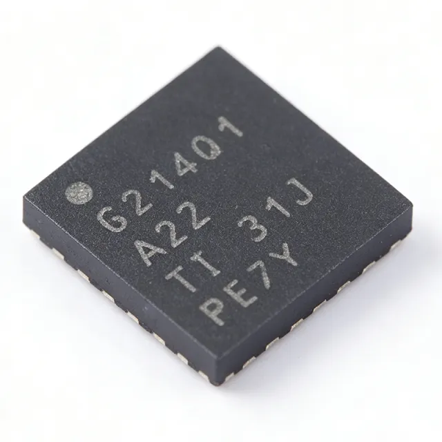
What Is the CDCE6214TWRGERQ1 and Why Do Engineers Choose It?
The CDCE6214TWRGERQ1 is a single-chip clock tree solution. A clock generator uses a phase-locked loop (PLL) to synthesize timing signals from a reference input, distributing synchronized clocks to processors, serial links, and data converters. This device integrates a configurable high-performance low-power fractional-N PLL that produces five independent clock outputs, selectable between various driver modes. It supports 100Ω systems, offers low electromagnetic emissions, and includes in-situ EEPROM programming via I2C, so you can configure the part on your own board without external programming hardware.
Engineers choose it because it consolidates multiple clock sources into one small, AEC-Q100-qualified package. The 4mm x 4mm VQFN with exposed pad fits space-constrained ECU designs, while medium-grade RMS jitter with spurs (specified over 12 kHz - 20 MHz for Fout > 100 MHz) supports reliable operation in high-speed serial links such as PCIe Gen 1-5.
How Do You Design In the CDCE6214TWRGERQ1? A Technical Guide
Power Supply and Decoupling
Operate the device from a single 3.3V supply. Ensure proper power supply decoupling with 0.1uF and 1uF capacitors placed close to the VDD pins (pins 1 and 17). Connect GND pins (2 and 18) to a solid ground plane, and solder the exposed pad for thermal and ground integrity.
Reference Inputs and Output Configuration
The device offers two clock inputs, IN0 (pin 3) and IN1 (pin 4), allowing redundant or switchable references. The four differential output pairs — OUT0/OUT0B (pins 5-6), OUT1/OUT1B (pins 7-8), OUT2/OUT2B (pins 9-10), and OUT3/OUT3B (pins 11-12) — are selectable between various driver modes, letting you match LVCMOS, LVPECL, LVDS, or other formats to your load. The device is designed for 100Ω systems, so route differential pairs with controlled 100Ω impedance.
Configuration and EEPROM
Configure the device through the I2C-compatible interface: SDA (pin 13) and SCL (pin 14) operate up to 400 kHz. The internal EEPROM holds two pages, and the SEL pin (pin 15) selects the active page externally — useful for two factory-programmed clock plans on one board. Program the EEPROM in-situ via I2C for flexible configuration without external programming hardware. The EN pin (pin 16) provides hardware enable control for power sequencing or low-power modes.
Thermal and Layout Considerations
The 24-VFQFN (4mm x 4mm) package with exposed pad suits dense layouts. Keep the PLL loop filter and reference traces short, and isolate output pairs from the reference to minimize crosstalk and EMI — the device's low EMI design helps, but good layout practice is still essential. [VERIFY_NEEDED: exact PCB layout recommendations beyond datasheet decoupling guidance]
What Are the Key Specifications at a Glance?
| Parameter | Value |
|---|---|
| Manufacturer | Texas Instruments |
| Category | Clock Generators |
| Output Frequency (max) | 350 MHz |
| Outputs | 4 differential |
| Inputs | 2 |
| PLL | 1 fractional-N |
| Supply Voltage | 3.3 V |
| Interface | I2C up to 400 kHz |
| EEPROM | 2 pages, external select pin |
| Package | 24-VFQFN (4mm x 4mm) |
| Operating Temperature | -40C to +125C |
| Jitter | Medium grade; RMS jitter with spurs 12 kHz - 20 MHz, Fout > 100 MHz |
| PCIe Support | Gen 1-5 |
| AEC-Q100 | Qualified |
| RoHS | Compliant |
| Lifecycle Status | Active |
| Price (as of 2026-09-04) | $4.50 (1 pc) to $2.88 (1000+ pcs) |
What Are the Best Alternatives and Drop-In Replacements?
Based on verified XAIPART data, two alternatives exist for the CDCE6214TWRGERQ1:
| Parameter | CDCE6214TWRGERQ1 | CDCE6214TWRGER | Si5338 |
|---|---|---|---|
| Type | Automotive Q1, AEC-Q100 qualified | Non-Q1 version, not AEC-Q100 qualified | Cross-brand (Skyworks) |
| Compatibility | Baseline | Pin-compatible, same functionality | Different programming interface; pin compatibility must be verified |
| Best Use | Automotive ADAS, infotainment | Industrial/commercial cost-optimized builds | Functional cross-brand option after verification |
| Price (as of 2026-09-04) | $4.50 (qty 1) to $2.88 (qty 1000) | [DATA_NEEDED: CDCE6214TWRGER pricing] | [DATA_NEEDED: Si5338 pricing] |
Summary: If your application does not require AEC-Q100, the CDCE6214TWRGER is the pin-compatible, likely more cost-effective drop-in. For higher performance from TI, the LMK5C33216RGCR is mentioned as an alternative but may require pinout verification. [DATA_NEEDED: LMK5C33216RGCR verified specifications]
Where Is This Component Used? Real Application Scenarios
The CDCE6214TWRGERQ1 serves six documented application areas:
- ADAS: Generates low-jitter clocks for ADAS processors, cameras, and radar modules; supports PCIe Gen 1-5 for high-speed sensor fusion data links.
- Automotive Infotainment: Provides clocks for audio DACs, USB controllers, and display interfaces with low EMI and programmable outputs.
- Industrial Automation: Clocks Ethernet, fieldbus, and processor interfaces in controllers and PLCs; the EEPROM allows pre-programmed configurations for quick deployment.
- Networking Equipment: Generates clocks for PCIe, Ethernet, and SerDes interfaces in switches and routers; multiple outputs reduce component count.
- Test and Measurement: Provides precise, programmable clocks for oscilloscopes and signal generators; the wide frequency range supports various test standards.
- Data Center: Low power consumption supports energy-efficient servers, storage, and networking with PCIe Gen 1-5 compatibility.
Example Design: A PCIe Gen 5 Clock Tree for an Automotive ECU
Problem: An ADAS domain controller needs four PCIe Gen 5 reference clocks plus a flexible auxiliary clock, in a space-constrained, AEC-Q100-qualified design.
Approach: Use one CDCE6214TWRGERQ1 as the single-chip clock tree. Feed a reference into IN0 (pin 3), configure the fractional-N PLL via I2C (pins 13-14) to synthesize the required frequencies up to 350 MHz, and drive four differential output pairs into 100Ω PCIe routing. Program two clock plans into the two EEPROM pages, using the SEL pin (pin 15) to switch configurations in production. Decouple both VDD pins (1 and 17) with 0.1uF and 1uF capacitors close to the pins.
Calculations: Frequency planning uses the fractional-N PLL; the exact PLL divider settings depend on the reference frequency chosen. [VERIFY_NEEDED: PLL divider equation and reference frequency ranges from the full TI datasheet]. Power budget relies on the device's ultra-low power consumption; exact current figures: [DATA_NEEDED: supply current per output mode].
Results: Four low-jitter differential clocks meeting PCIe Gen 1-5 requirements from a single 4mm x 4mm device, AEC-Q100 qualified for -40C to +125C, with in-situ EEPROM reprogrammability for field updates.
What Is the Market Position, Lifecycle, and Supply Situation?
The CDCE6214TWRGERQ1 is in active lifecycle status. XAIPART currently lists 99,999 units in stock with MOQ 1 and tiered pricing from $4.50 (qty 1) down to $2.88 (qty 1000) as of 2026-09-04. [DATA_NEEDED: manufacturer lifecycle forecast, last time buy date, and long-term supply commitments]. [DATA_NEEDED: competitor market share and demand trend data for automotive clock generators].
What Should Buyers Watch Next? Trends and Outlook
Anchor your purchasing decisions to these verified facts: the device supports PCIe Gen 1-5, so it covers current and next-generation serial links without redesign. The AEC-Q100 qualification and -40C to +125C rating position it for the growing automotive electronics market. Watch three things: (1) pricing tiers — volume buyers capture a 36% unit-cost reduction at 1,000 pieces versus single-unit pricing as of 2026-09-04; (2) the non-Q1 CDCE6214TWRGER as a cost-down path for industrial designs sharing the same PCB; and (3) higher-performance TI alternatives such as the LMK5C33216RGCR if jitter requirements tighten, with pinout verification. [VERIFY_NEEDED: PCIe Gen 6 and emerging standard support roadmap for the CDCE6214 family]. With 99,999 units in stock and active lifecycle status, near-term supply risk on XAIPART is low.
Comments
Be the first to comment.
🔐 Please sign in to post a comment.
Don't have an account? Sign up