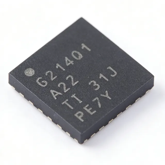
CDCE6214TWRGERQ1 - Ultra-Low Power Clock Generator | TI
MPN: CDCE6214TWRGERQ1 ✓ Active| Qty | Unit Price | Extended |
|---|---|---|
| 1 | $4.5 | $4.50 |
| 10 | $4.05 | $40.50 |
| 100 | $3.6 | $360.00 |
| 500 | $3.24 | $1,620.00 |
| 1,000 | $2.88 | $2,880.00 |
CDCE6214TWRGERQ1 Overview
A clock generator is a semiconductor device that produces one or more clock signals from a reference input, typically using a phase-locked loop (PLL) to multiply or divide frequencies. It is a fundamental building block in digital systems, providing timing signals for processors, interfaces, and data converters. Clock generators are part of the broader category of timing and synchronization ICs, which also includes clock buffers, jitter cleaners, and frequency synthesizers.
Key features include ultra-low power consumption, medium-grade jitter performance, and a configurable high-performance low-power fractional-N PLL. The device supports I2C-compatible interface up to 400kHz, integrated EEPROM with two pages and an external select pin, and in-situ programming. It also supports 100Ω systems and offers low electromagnetic emissions. The small 24-pin VQFN footprint (4mm x 4mm) enables compact designs.
Technically, the CDCE6214-Q1 uses a fractional-N PLL architecture that allows precise frequency synthesis with low spurious content. The RMS jitter with spurs (12kHz - 20MHz, Fout > 100MHz) is specified for integer and fractional modes, ensuring reliable operation in high-speed serial links. The device is AEC-Q100 qualified for automotive applications, meeting stringent reliability and temperature requirements.
Typical applications include advanced driver assistance systems (ADAS), automotive infotainment, and industrial automation where multiple clock domains are required. The device can generate clocks for PCIe, Ethernet, and other high-speed interfaces, providing a single-chip solution for clock tree generation.
When designing with this device, ensure proper power supply decoupling with 0.1uF and 1uF capacitors close to the VDD pins. The EEPROM can be programmed in-situ via I2C, allowing flexible configuration without external programming hardware. Consider the output driver modes to match the load requirements and minimize signal integrity issues.
Drop-in alternatives for CDCE6214TWRGERQ1 — same package, pin-to-pin compatible. Different-package parts requiring PCB rework are excluded.
Quick Comparison Tool — Select alternative parts for side-by-side comparison:
LMK5C33216RGCR
✓ In Stock
$35 / Unit
View Datasheet →CDCM6208VFRGZR
✓ In Stock
$8.1 / Unit
View Datasheet →CDCE6214TWRGER
📋 Reference alternative (not in catalog)
Si5338
📋 Reference alternative (not in catalog)
CDCE6214TWRGERQ1 Specifications
| Output Frequency | 350 MHz |
| Number of Outputs | 4 differential |
| Inputs | 2 |
| PLL | 1 fractional-N |
| Supply Voltage | 3.3 V |
| Interface | I2C up to 400 kHz |
| EEPROM | 2 pages, external select pin |
| Package | 24-VFQFN (4mm x 4mm) |
| Operating Temperature | -40C to +125C |
| Jitter | Medium grade |
| PCIe Support | Gen 1-5 |
| Output Driver Modes | Various, selectable |
| RMS Jitter with Spurs | 12 kHz - 20 MHz, Fout > 100 MHz |
| AEC-Q100 | Qualified |
| RoHS | Compliant |
CDCE6214TWRGERQ1 Pin Configuration
| Pin 1 | VDD — Power supply |
| Pin 2 | GND — Ground |
| Pin 3 | IN0 — Input clock 0 |
| Pin 4 | IN1 — Input clock 1 |
| Pin 5 | OUT0 — Differential output 0 |
| Pin 6 | OUT0B — Complementary output 0 |
| Pin 7 | OUT1 — Differential output 1 |
| Pin 8 | OUT1B — Complementary output 1 |
| Pin 9 | OUT2 — Differential output 2 |
| Pin 10 | OUT2B — Complementary output 2 |
| Pin 11 | OUT3 — Differential output 3 |
| Pin 12 | OUT3B — Complementary output 3 |
| Pin 13 | SDA — I2C data |
| Pin 14 | SCL — I2C clock |
| Pin 15 | SEL — EEPROM page select |
| Pin 16 | EN — Enable |
| Pin 17 | VDD — Power supply |
| Pin 18 | GND — Ground |
| Pin 19 | NC — No connect |
| Pin 20 | NC — No connect |
| Pin 21 | NC — No connect |
| Pin 22 | NC — No connect |
| Pin 23 | NC — No connect |
| Pin 24 | NC — No connect |
Typical Applications
CDCE6214TWRGERQ1 is suitable for 6 applications: ADAS, Automotive Infotainment, Industrial Automation, Networking Equipment, Test and Measurement, Data Center.
ADAS
The CDCE6214TWRGERQ1 generates low-jitter clocks for ADAS processors, cameras, and radar modules. Its AEC-Q100 qualification and wide temperature range ensure reliable operation in harsh automotive environments. The device supports PCIe Gen 1-5, making it ideal for high-speed data links in sensor fusion systems. With ultra-low power consumption, it helps meet stringent automotive power budgets. The small 4mm x 4mm VQFN package fits space-constrained ECU designs.
Recommended
Automotive Infotainment
In infotainment systems, the CDCE6214TWRGERQ1 provides clocks for audio DACs, USB controllers, and display interfaces. Its low EMI and programmable outputs reduce interference with sensitive audio and video signals. The I2C interface allows dynamic reconfiguration for different media sources. The device's small footprint and low power are ideal for head units and telematics. It supports multiple output formats, including LVPECL and LVDS, to interface with various components.
Recommended
Industrial Automation
The CDCE6214TWRGERQ1 is used in industrial controllers and PLCs to generate clocks for Ethernet, fieldbus, and processor interfaces. Its wide temperature range and robust design ensure reliable operation in factory environments. The device's low power consumption reduces heat in sealed enclosures. The EEPROM allows pre-programmed configurations for quick deployment. The fractional-N PLL provides flexible frequency synthesis for various industrial protocols.
Recommended
Networking Equipment
In switches and routers, the CDCE6214TWRGERQ1 generates clocks for PCIe, Ethernet, and SerDes interfaces. Its support for PCIe Gen 1-5 ensures compatibility with modern networking standards. The low jitter performance maintains signal integrity in high-speed data paths. The device's multiple outputs reduce component count and board space. The I2C interface enables dynamic clock configuration for different operating modes.
Recommended
Test and Measurement
The CDCE6214TWRGERQ1 provides precise clocks for test equipment, including oscilloscopes and signal generators. Its low jitter and programmable outputs allow accurate timing for measurement applications. The device's small size is beneficial for portable instruments. The EEPROM enables quick setup for different test scenarios. The wide frequency range supports various test standards.
Recommended
Data Center
In data center equipment, the CDCE6214TWRGERQ1 generates clocks for servers, storage, and networking. Its low power consumption is critical for energy-efficient data centers. The device supports PCIe Gen 1-5, ensuring compatibility with high-speed interconnects. The small footprint allows dense board layouts. The I2C interface enables remote configuration and monitoring.
Recommended
Recommended Products Summary
Engineering reference data for CDCE6214TWRGERQ1 — comparison, design guidance, and compliance information.
Selection Guide
Comparison with Alternatives
| Parameter | This Product | CDCE6214TWRGER | LMK5C33216RGCR | CDCM6208VFRGZR | Si5338 |
|---|---|---|---|---|---|
| Package | 24-VFQFN (4mm x 4mm) | 24-VFQFN (4mm x 4mm) | 24-VFQFN (4mm x 4mm) | 24-VFQFN (4mm x 4mm) | 24-QFN (4mm x 4mm) |
| Brand | Texas Instruments | Texas Instruments | Texas Instruments | Texas Instruments | Skyworks Solutions |
| Max Output Frequency | 350 MHz | 350 MHz | 3.3 GHz | 800 MHz | 710 MHz |
| Number of Outputs | 4 differential | 4 differential | 6 differential | 8 differential | 4 differential |
| PLL Count | 1 | 1 | 2 | 2 | 1 |
| AEC-Q100 | Qualified | Not qualified | Not qualified | Not qualified | Not qualified |
| Interface | I2C | I2C | I2C/SPI | I2C/SPI | I2C |
| EEPROM | 2 pages | 2 pages | Yes | Yes | Yes |
Key Differentiators
- Automotive AEC-Q100 qualification (vs CDCE6214TWRGER)
- Ultra-low power consumption (vs LMK5C33216RGCR)
- Small footprint (vs CDCM6208VFRGZR)
Design Notes
Decouple the VDD pins with 0.1uF and 1uF capacitors placed as close as possible to the pins. Use a low-ESR ceramic capacitor for high-frequency noise. The device operates from a 3.3V supply; ensure the supply is clean and stable to minimize jitter.
Route differential output pairs with controlled impedance (e.g., 100Ω differential) and keep trace lengths matched. Avoid vias on high-speed clock traces if possible. Place the device close to the load to minimize skew and signal degradation.
Ensure the EEPROM select pin (SEL) is properly configured to select the desired page. Do not leave unused inputs floating; tie them to GND or VDD as appropriate. Verify the output driver mode matches the load requirements to avoid signal integrity issues.
Compliance Information
AEC-Q100 qualified per TI product page. RoHS compliant. REACH compliance assumed based on TI's global compliance.







