The Intel (formerly Altera) EPC2LC20N is a 1.6-Mbit in-system programmable Flash configuration PROM that stores the bitstream for SRAM-based LUT FPGAs and reloads it into the target device at every power-up. It ships in a 20-pin PLCC (J-lead, 9x9 mm) surface-mount package, operates from dual supplies of 3.0 V to 3.6 V (VCCINT) and 4.75 V to 5.25 V (VCCIO), supports JTAG-ISP per IEEE 1149.1 / IEEE 1532, and runs the configuration clock up to 8 MHz using its internal oscillator. The part is available now on XAIPART with 99,999 units in stock, MOQ of 1, and tiered pricing from $12.50 (qty 1) down to $7.40 (qty 1000) as of 2026-09-12. Intel has marked the EPC2 family NRND (Not Recommended for New Designs), so new designs should evaluate the drop-in EPC2LI20N industrial-grade variant or newer density upgrades such as the EPC2LC40N.
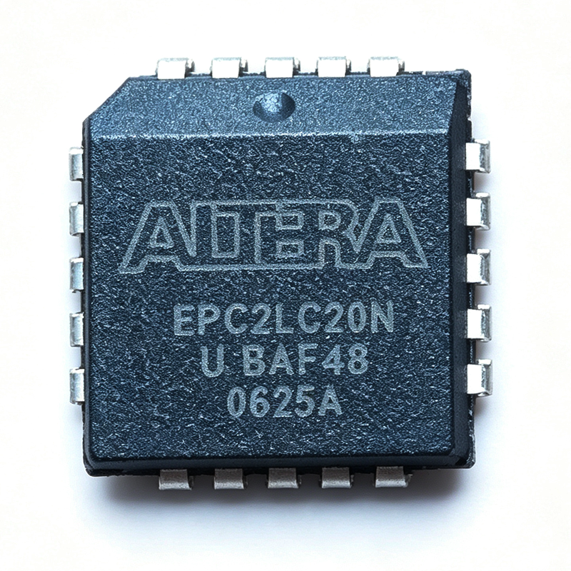
What Is the EPC2LC20N and Why Do Engineers Still Specify It?
SRAM-based FPGAs are volatile: they lose their configuration at every power-down. A configuration PROM is the non-volatile serial memory that holds the bitstream and streams it into the FPGA on each boot. The EPC2LC20N performs that single-chip boot role, replacing discrete EPROM, microcontroller, or boot-PROM arrangements in the Altera/Intel power-on sequencing hierarchy (CPLD -> glue logic -> PROM -> FPGA).
The key verified specifications are:
| Parameter | Value (verified) |
|---|---|
| Function | In-System Programmable Configuration PROM for SRAM-based FPGAs |
| Memory Size | 1.6 Mbit |
| Memory Type | Flash |
| Programmable Type | In System Programmable (ISP) |
| VCCINT | 3.0 V to 3.6 V |
| VCCIO | 4.75 V to 5.25 V |
| Configuration Clock (max) | 8 MHz (internal oscillator) |
| JTAG Support | IEEE 1149.1 / IEEE 1532 compliant |
| Package | 20-pin PLCC (J-Lead, 9x9 mm), surface mount |
| Packaging | Tube |
| Supported FPGA Families | Altera APEX, Cyclone, Stratix, ACEX, MAX 7000 |
| Commercial Temperature | 0 C to +70 C (per EPC2 family grade, FAQ) |
The dual-rail supply is the standout feature: the 4.75 V to 5.25 V VCCIO lets the PROM bridge legacy 5 V support circuitry with 3.3 V FPGA I/O on the same PCB, which is why the part persists in industrial, telecom, and military/aerospace retrofit designs.
How Do You Design In and Program the EPC2LC20N?
Serial configuration interface. The PROM uses a 4-pin serial interface (DATA0, DCLK, nCONFIG, nSTATUS) plus CONF_DONE to handshake with the target FPGA. The nCONFIG, nSTATUS, and CONF_DONE handshake eliminates external glue logic in most designs. The internal 8 MHz oscillator removes the need for an external clock source; faster configuration is supported when the target FPGA supplies an external DCLK. Multiple EPC2 PROMs can be cascaded in series to configure FPGAs whose bitstreams exceed 1.6 Mbit, and the PROM automatically negotiates baud rate with the target device.
JTAG in-system programming. The EPC2LC20N supports JTAG-ISP per IEEE 1149.1 / IEEE 1532. Engineers re-flash the bitstream on a populated board with the Altera/Intel Quartus Programmer or a compatible JTAG loader, no desoldering required. This enables field firmware upgrades and speeds prototyping. Respect JTAG chain order if multiple PROMs are cascaded.
Power and layout. Both supply rails require 0.1 uF + 10 uF decoupling placed as close as possible to the IC pins. The 5 V rail tolerance simplifies mixed-voltage designs.
Key pinout (functional pins):
| Pin | Name | Function |
|---|---|---|
| 1 | DATA0 | Configuration data output to target FPGA |
| 2 | DCLK | Configuration clock input/output |
| 3 | nCONFIG | Configuration control input (active low) |
| 4 | nSTATUS | Configuration status output (active low) |
| 5 | CONF_DONE | Configuration complete output |
| 6-9 | TCK/TMS/TDI/TDO | JTAG test clock, mode select, data in, data out |
| 10 | VCCINT | 3.3 V core supply (3.0 V to 3.6 V) |
| 11 | GND | Ground |
| 12 | VCCIO | 5 V I/O supply (4.75 V to 5.25 V) |
| 13-16 | OE/CE/MODE/RESET | Output enable, chip enable, mode select, reset |
The full pin-by-pin description lives on the EPC2LC20N product page.
Boot-time check. At the 8 MHz maximum DCLK, a full 1.6 Mbit image loads in roughly 200 ms, fast enough for most industrial power-on sequencing requirements.
Selection rules of thumb:
- Bitstream fits in 1.6 Mbit (e.g., Cyclone EP1C3/EP1C6/EP1C12, APEX EP20K60/EP20K100, ACEX EP1K100): one EPC2LC20N suffices.
- Larger Stratix-class images: cascade EPC2 devices or step up to the 4 Mbit EPC2LC40N in the same footprint.
- Field temperature below 0 C or above +70 C: use the industrial-grade EPC2LI20N (-40 C to +85 C), a drop-in replacement.
- Socketed legacy PLC and card-swap repairs: PLCC-20 sockets allow field replacement without soldering.
Which Alternatives Can Replace the EPC2LC20N?
Within the verified XAIPART database, the closest drop-in alternatives are same-footprint EPC2 family members:
| Parameter | EPC2LC20N | EPC2LC8N | EPC2LC40N | EPC2LI20N |
|---|---|---|---|---|
| Density | 1.6 Mbit | 0.8 Mbit (-50%) | 4 Mbit (+150%) | 1.6 Mbit |
| Package | 20-PLCC (9x9 mm) | Same PLCC-20 footprint | Same PLCC-20 footprint | Same 20-pin PLCC package |
| JTAG-ISP | IEEE 1149.1 / IEEE 1532 | Same JTAG-ISP | Same JTAG-ISP | Same JTAG-ISP interface |
| Temperature grade | Commercial (0 C to +70 C) | [DATA_NEEDED: EPC2LC8N temperature] | [DATA_NEEDED: EPC2LC40N temperature] | Industrial (-40 C to +85 C) |
| Best for | Reference density for Cyclone/APEX/ACEX | Smaller bitstreams (drop-in downgrade) | Bitstreams over 1.6 Mbit (Stratix-class) | Drop-in replacement for harsh environments |
Substitution logic: the EPC2LC8N can replace the EPC2LC20N only when the bitstream is 0.8 Mbit or smaller; the reverse is never true, since 0.8 Mbit cannot hold a 1.6 Mbit image. The EPC2LC40N is the closest density upgrade within the same footprint. The EPC2LI20N is the best drop-in replacement when only the temperature grade differs, sharing the same 1.6 Mbit Flash, 8 MHz clock, and JTAG-ISP interface. For genuinely new designs, Intel directs buyers to the EPCQ-series (e.g., EPCQ4SI8N, EPCQ16SI8N) or the FPGA's built-in flash.
What Is the Market Position and Supply Situation for the EPC2LC20N?
Intel has flagged the EPC2LC20N as NRND (Not Recommended for New Designs) as of 2026-09-11. The part remains orderable for existing designs and spares, and distributors still hold inventory: Wolfchip Electronics lists 35,090 pcs (as of Jul 22, 2026), icDirectory lists 2,350 pcs (as of Oct 13, 2025), and Avaq also carries stock. XAIPART itself shows 99,999 units available with MOQ 1, at $12.50 (qty >= 1), $11.25 (qty >= 10), $9.80 (qty >= 100), $8.65 (qty >= 500), and $7.40 (qty >= 1000) as of 2026-09-12.
Lead time from authorized distributors is typically 4 to 8 weeks as of 2026-09-11. Because the family is NRND, stock levels are declining and lead times are extending. RoHS compliance is not explicitly confirmed in the datasheet provided; the part ships in tube packaging with a lead-containing 20-PLCC J-lead package, and many legacy PLCC Altera PROMs are non-RoHS. Verify RoHS status on the distributor product page before committing it to a RoHS-only BOM.
What Should Buyers Watch Next for the EPC2LC20N?
Three trends anchored to the verified data deserve attention:
- NRND risk management. With Intel steering new designs to EPCQ-series PROMs and FPGA-internal flash, EPC2 inventory will keep thinning. Production programs should qualify the EPC2LI20N or EPC2LC40N now, since both share the exact PLCC-20 footprint and JTAG-ISP interface of the EPC2LC20N, making requalification largely a temperature/density review rather than a layout change.
- Last-time-buy planning. At $7.40 per unit at 1000-piece quantities (as of 2026-09-12) and 99,999 units on XAIPART, spare-pool provisioning is still inexpensive. Buyers supporting PLC, base-station, and military retrofit fleets should size their lifetime buy against the 4-to-8-week lead-time trend.
- Legacy 5 V ecosystem persistence. The 4.75 V to 5.25 V VCCIO tolerance keeps the EPC2LC20N relevant wherever 5 V backplanes and boundary-scan (IEEE 1149.1) test requirements persist. Any migration to EPCQ-series devices must account for their different supply and package (e.g., SOIC-8), which is not footprint-compatible with the PLCC-20.
Engineers continuing with the part should anchor designs to its core verified facts: 1.6 Mbit Flash, 8 MHz max DCLK with internal oscillator, dual 3.0-3.6 V / 4.75-5.25 V rails, JTAG-ISP per IEEE 1149.1 / IEEE 1532, and the PLCC-20 (9x9 mm) J-lead package. Browse the full EPC2LC20N listing, compare the EPC2LC40N density upgrade, or explore XAIPART's Memory ICs catalog and FPGA configuration guides for adjacent design resources.
Comments
Be the first to comment.
🔐 Please sign in to post a comment.
Don't have an account? Sign up