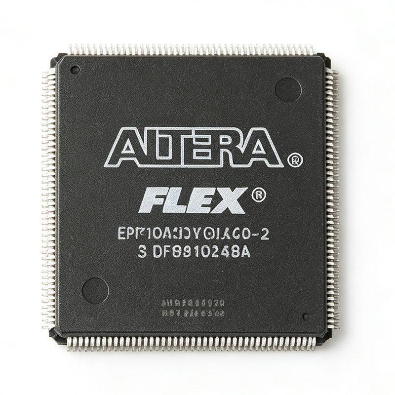
Quick Answers: What Is the EPF10K50VQI240-2 and Is It in Stock?
The EPF10K50VQI240-2 is an Altera (now Intel) FLEX 10K SRAM-based field-programmable gate array with 50,000 typical gates, 2,880 logic elements (LEs) inside 360 Logic Array Blocks, 20,480 bits of embedded EAB memory, and 189 maximum user I/O pins in a 240-pin PQFP package. It runs a 3.3 V core at up to 125 MHz internal frequency with a 0.6 ns propagation delay, is fabricated on a 0.42 µm CMOS process, and supports JTAG (IEEE 1149.1) boundary scan. XAIPART's verified database lists 99,999 units in stock with an MOQ of 1 and a base price of $357.9545 as of 2026-09-16.
The combination of a 3.3 V core, I/O banks that can run at 5.0 V, 3.3 V, or 2.5 V, and a gull-wing PQFP that a technician can rework by hand makes this part a mixed-voltage glue-logic device for legacy industrial control, telecom interface, PCI bridging, and test-and-measurement boards. This guide consolidates the verified specification table, the functionally key pins, same-package alternatives, and the supply picture so you can qualify or replace the device without re-reading the entire FLEX 10K datasheet.
Verified specification summary
| Parameter | Verified value |
|---|---|
| Family | FLEX 10K |
| Manufacturer | Altera (now Intel) |
| Typical gates | 50,000 |
| Logic Elements (LEs) | 2,880 |
| Logic Array Blocks (LABs) | 360 |
| Embedded memory | 20,480 bits |
| Maximum user I/O | 189 |
| Maximum internal frequency | 125 MHz |
| Propagation delay | 0.6 ns |
| Process technology | 0.42 µm CMOS |
| Core supply voltage | 3.3 V |
| Operating temperature | 0 °C to +70 °C |
| Package | 240-pin BFQFP / PQFP (gull-wing), package code FQFP, surface mount |
| Configuration interface | Passive Serial / Fast Passive Parallel (JTAG) |
| Speed grade | -2 |
| RoHS status | Compliant (lead-free PQFP variant) |
| JTAG | IEEE 1149.1 supported |
One caveat before you design in this device: the source records conflict on lifecycle and price. The XAIPART product record lists the part as active with 99,999 units on hand, while the distributor-derived FAQ records describe the FLEX 10K family as obsolete / last-time-buy and quote unit prices in the $27 to $42 range. Both discrepancies are flagged for verification and should be confirmed with your distributor before you commit to a production build.
Technical Guide: How Do You Design the EPF10K50VQI240-2 Into a Board?
The FLEX 10K architecture pairs a fine-grained logic fabric with coarse-grained Embedded Array Blocks. Each of the 360 LABs holds eight LEs, which yields the documented 2,880 LEs, and each EAB can be configured as synchronous RAM, ROM, or a 4-bit × 4-bit multiplier in arithmetic mode. The chip-wide FastTrack interconnect routes signals between LABs and I/O elements. That dual-grained structure is why the device handles LUT-based datapath logic and memory-intensive state machines on one die, and it drives every design decision below.
Step 1 — Power the 3.3 V core and set each I/O bank independently
VCCINT is a 3.3 V rail (3.3 V ±10%). Every I/O bank has its own VCCIO rail and can be powered independently to interface with 5.0 V, 3.3 V, or 2.5 V peripherals. Place a 100 nF decoupling capacitor at each supply pin plus a 10 µF bulk capacitor within 5 mm of every VCC pin. Because the banks are independent, one board can mix a 5 V optocoupler front end, 3.3 V bus logic, and 2.5 V memory without external level shifters — the main reason this part stayed in mixed-voltage industrial designs long after faster FPGAs appeared.
Step 2 — Choose the configuration path before layout
The EPF10K50VQI240-2 supports Passive Serial (PS), Passive Parallel Synchronous (PPS), Passive Parallel Asynchronous (PPA), and JTAG configuration. Configuration data is typically stored in an Altera EPC2 or EPC16 configuration EPROM or loaded over JTAG with a download cable such as the ByteBlasterMV or USB-Blaster. Fast Passive Parallel (FPP) mode moves configuration data over an 8-bit-wide bus for the fastest load times. Reserve these dedicated pins in your netlist: nCONFIG (pin 221), nSTATUS (pin 220), DCLK (pin 222), and DATA0 (pin 223) for configuration, and TCK (pin 200), TDI (pin 201), TDO (pin 202), and TMS (pin 203) for the JTAG chain.
Step 3 — Budget I/O against the 240-pin PQFP
The 240-pin BFQFP/PQFP carries a maximum of 189 user I/O pins, or 78.75% of the package pins, leaving the remainder for VCCINT, VCCIO, ground, JTAG, and configuration signals. Some distributor listings quote 274 I/Os; that figure corresponds to a different package variant, not the 240-pin PQFP, where 189 is the canonical maximum. The package body is approximately 32 × 32 mm with 0.5 mm lead pitch and gull-wing leads. That pitch is hand-reworkable, which matters for repairing fielded equipment, but it also caps routing density and rules out high-speed differential signaling above roughly 100 MHz. Use this part for moderate-speed glue logic, not SERDES-class interfaces.
Step 4 — Close timing with the -2 speed grade
The -2 speed grade delivers a maximum internal frequency of 125 MHz with a 0.6 ns propagation delay. At 125 MHz the clock period is 8 ns, so a single 0.6 ns combinatorial path consumes 7.5% of the period before routing, clock skew, and setup overhead are added. Treat 125 MHz as a ceiling for simple registered logic, not a blanket operating point: memory-intensive EAB paths and wide bus decode logic will close timing at lower frequencies. The 20,480 bits of embedded memory equal 2,560 bytes — enough for small FIFO buffers, microcode stores, or bus-state tables, but not for large packet buffers.
Step 5 — Plan the migration before you commit
Porting a FLEX 10K design to a current production family is a board redesign, not a socket swap. MAX II CPLDs (EPM240, EPM570) are smaller in density and pin-compatible only with some legacy PLDs, while Cyclone IV/V FPGAs use BGA packages and require full PCB rework. Budget engineering time for re-synthesis, pin remapping, and re-qualification if the product has more than a few years of life left. Confirmed drop-in candidates inside the FLEX 10K family are covered in the next section.
Key pins to route first
| Pin | Name | Function |
|---|---|---|
| 120 | VCCINT | 3.3 V core supply |
| 180 | VCCIO | I/O bank supply voltage |
| 60 | GND | Ground reference |
| 221 | nCONFIG | Configuration start (active low) |
| 220 | nSTATUS | Configuration status (open-drain) |
| 222 | DCLK | Configuration clock |
| 223 | DATA0 | Configuration data input (PS mode) |
| 200 | TCK | JTAG test clock |
| 201 | TDI | JTAG test data in |
| 202 | TDO | JTAG test data out |
| 203 | TMS | JTAG test mode select |
| 1, 240 | I/O | User I/O pins (bank-dependent voltage) |
The full 240-pin table lives on the EPF10K50VQI240-2 product page; the pins above are the ones that drive layout constraints and configuration sequencing.
Alternatives & Comparison: What Are the Drop-In Options for the EPF10K50VQI240-2?
Same-family, same-package parts are the only true drop-in path for this device. The table below compares the EPF10K50VQI240-2 with the same 240-pin PQFP FLEX 10K options documented in the verified records. Cells marked [DATA_NEEDED] are not covered by the source data.
| Parameter | EPF10K50VQI240-2 | EPF10K50VQC240-3N | EPF10K50VQC240-1N | EPF10K50EQC240-2 |
|---|---|---|---|---|
| Family | FLEX 10K | FLEX 10K | FLEX 10K | FLEX 10KE |
| Core supply (VCCINT) | 3.3 V | 3.3 V | [DATA_NEEDED: VCCINT for EPF10K50VQC240-1N] | 2.5 V |
| Speed grade | -2 | -3 | -1 | -2 |
| Maximum internal frequency | 125 MHz | 90 MHz | 166 MHz | [DATA_NEEDED: max internal frequency for EPF10K50EQC240-2] |
| Typical gates | 50,000 | 50,000 (same FLEX 10K die) | [DATA_NEEDED: typical gates for EPF10K50VQC240-1N] | [DATA_NEEDED: typical gates for EPF10K50EQC240-2] |
| Process technology | 0.42 µm CMOS | [DATA_NEEDED: process technology for EPF10K50VQC240-3N] | [DATA_NEEDED: process technology for EPF10K50VQC240-1N] | 0.25 µm |
| Package | 240-pin PQFP | 240-pin PQFP | 240-pin PQFP | 240-pin PQFP |
| Pin-to-pin compatible with EPF10K50VQI240-2 | Reference part | Yes — functionally identical, slower | Same package, higher speed option | No — different voltage and I/O bank structure |
| Lead-free assembly | Yes (lead-free PQFP variant) | Yes (N suffix) | Yes (N suffix) | [DATA_NEEDED: RoHS status for EPF10K50EQC240-2] |
The EPF10K50VQC240-3N is the safest drop-in: same 240-pin PQFP, same 3.3 V core, same 50,000-gate FLEX 10K die, and lead-free assembly. The only functional difference is speed — 90 MHz versus 125 MHz — so any design that already closes timing with margin below 90 MHz ports without change. If you need more headroom than the -2 grade provides, the EPF10K50VQC240-1N offers a -1 speed grade at 166 MHz in the same package, making it the upgrade path when the -2 grade is the bottleneck.
The EPF10K50EQC240-2 looks like a candidate on paper because it shares the 240-pin PQFP, but it belongs to the 2.5 V FLEX 10KE family built on a 0.25 µm process with a different I/O bank structure. It is not pin-to-pin compatible and cannot be dropped into a FLEX 10K socket without a board revision. Outside the family, MAX II CPLDs and Cyclone IV/V FPGAs change both package and pinout, so they are migration targets rather than alternatives.
Related search: EPF10K50VQC240-3N availability. Lifecycle and stock records for these same-package parts are not included in the verified alternatives data and remain a gap: [DATA_NEEDED: same-package alternative stock, lifecycle, and price records].
Industry Insight: What Is the Lifecycle and Supply Situation?
Two verified commercial figures frame the buy decision. XAIPART's database reports 99,999 units available with an MOQ of 1, and tiered pricing that falls steeply with volume as of 2026-09-16:
| Quantity | Unit price (as of 2026-09-16) |
|---|---|
| 1+ | $613.6364 |
| 10+ | $443.1818 |
| 100+ | $392.0455 |
| 500+ | $375.00 |
| 1000+ | $357.9545 |
Moving from the 1-piece price to the 1,000-piece price reduces unit cost by 41.7%, which is the strongest argument for consolidating demand into a single buy rather than placing repeat small orders.
Lifecycle status is the unresolved question. The XAIPART product record lists the EPF10K50VQI240-2 as active, while the distributor-derived FAQ records for this family state that Altera (now Intel FPGA) has discontinued the FLEX 10K family and classify the part as obsolete / last-time-buy, with recommended migration to MAX II, MAX V, Cyclone IV/V, or Lattice MachXO2/XO3. Both statements appear in the source data and cannot both be correct, so confirm the current status with your distributor and record the answer in your approved-vendor list. The underlying limitation applies regardless of the label: no new silicon is being designed into this family, so treat supply as finite.
Lead time is quoted on request because the part is no longer in active production. Documented behavior for obsolete FPGAs ranges from immediate shipment when stock sits on a distributor shelf to 8–12 weeks for last-time-buy orders placed through the manufacturer. Distributor-level stock breakdown by region or warehouse is not in the verified data: [DATA_NEEDED: distributor stock and lead-time breakdown]. The Altera PCN number and date backing the obsolescence claim are also absent: [DATA_NEEDED: PCN document number and publication date].
A second conflict affects budget planning. The FAQ records quote approximately $42.50 at quantity 1 and $27.40 at quantity 1000 as of 2026-09-11, which is roughly an order of magnitude below the XAIPART tier table above. Reconcile the two before you commit purchase-order funding, and treat the higher figure as the conservative planning number. See the FPGA & CPLD category for current listings across both sources.
Trends & Outlook: What Should Buyers Watch?
Mixed-voltage interfaces keep this part relevant. The 3.3 V core with independently powered I/O banks supporting 5.0 V, 3.3 V, and 2.5 V is the reason the EPF10K50VQI240-2 still appears in sustaining designs. Boards built around 5 V optocouplers, relays, and sensor front ends avoid level-shifter BOM cost when this FPGA does the translation.
DSP functions have moved on-die, but the EAB multiplier still works. Each EAB can act as a 4-bit × 4-bit multiplier, and cascading EABs builds 8 × 8 or 16 × 16 multipliers for FIR-filter and FFT butterfly datapaths. Modern Cyclone IV devices integrate hardware multipliers, so future designs should plan the arithmetic in dedicated DSP blocks rather than fabric.
Package physics cap the ceiling. The 240-pin PQFP at 0.5 mm pitch on a 32 × 32 mm body limits routing density and rules out high-speed differential signaling beyond roughly 100 MHz. Any roadmap that needs SERDES or DDR interfaces leaves this package behind.
Configuration memory is the silent dependency. The device is SRAM-based, so every board needs an EPC2 or EPC16 configuration EPROM or a JTAG load path with a ByteBlasterMV or USB-Blaster cable. When FLEX 10K supply tightens, configuration-EEPROM supply tightens with it — qualify both parts together.
Buy lifecycle risk deliberately. With 99,999 units on hand at an MOQ of 1 and volume pricing at $357.9545 as of 2026-09-16, a last-time-buy buffer is affordable; the expensive mistake is discovering a shortage mid-build. Pair that with a qualified migration path to MAX V, Cyclone IV/V, or MachXO2/XO3, and validate every order through the EPF10K50VQI240-2 product page. Supported EDA tool versions for ongoing design maintenance are outside the verified data: [DATA_NEEDED: supported EDA tool versions and device library status]. For a broader framework, see our FPGA lifecycle and migration guide.
Comments
Be the first to comment.
🔐 Please sign in to post a comment.
Don't have an account? Sign up