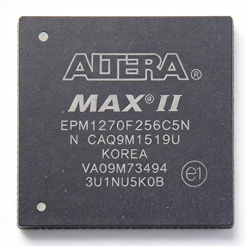
What Is the EPM1270F256C5N and Why Do Engineers Choose It?
The Intel/Altera EPM1270F256C5N is a 980-macrocell, non-volatile, instant-on CPLD from the MAX II family, housed in a 256-ball FineLine BGA (256-FBGA) package. It integrates 1270 logic elements, 212 user I/O pins, a 6.2 ns pin-to-pin propagation delay (tPD), and a 201.1 MHz maximum internal frequency, with dual 2.5 V / 3.3 V internal supply support on a 0.18-µm process. As of 2026-09-12, the part is active in the lifecycle, stocked at XAIPART with 99,999 units available, MOQ 1, priced from $28.50 at qty 1 down to $16.20 at qty 1000. The 'N' suffix denotes a lead-free (Pb-free) finish.
A CPLD (Complex Programmable Logic Device) is a non-volatile programmable logic IC that combines AND/OR array-based macrocell architecture with on-chip flash configuration memory, delivering instant-on behavior at power-up without an external boot ROM. In the programmable logic hierarchy, CPLDs sit between small SPLDs/GALs and larger FPGAs. MAX II CPLDs added low power via a multi-core architecture with internal flash, 8 Kbits of user flash memory (per MAX II family), and a JTAG-based in-system programming (ISP) interface, making them a preferred choice for cost-sensitive control-plane logic such as glue logic, I/O expansion, bus bridges, and power-up sequencers.
What Are the Key Specifications of the EPM1270F256C5N?
All values below are verified from the XAIPART product database and the Altera MAX II family datasheet.
| Parameter | EPM1270F256C5N |
|---|---|
| Series / Family | MAX II / EPM1270 |
| Device Type | CPLD (Complex Programmable Logic Device) |
| Macrocells | 980 |
| Logic Elements | 1270 |
| User I/O | 212 |
| Pin-to-Pin Delay (tPD) | 6.2 ns |
| Maximum Frequency (fMAX) | 201.1 MHz |
| Internal Supply Voltage | 2.5 V / 3.3 V |
| Operating Temperature | 0°C to 85°C (TJ) |
| Process Technology | 0.18 µm |
| Configuration | Non-volatile flash, in-system programmable |
| Programming Interface | JTAG (IEEE 1149.1) / ISP |
| Package / Case | 256-FBGA (1.0 mm ball pitch) |
| Mounting Type | Surface Mount |
| Lead Finish | Pb-free ('N' suffix) |
Beyond the headline numbers, the device supports multi-voltage I/O, a chip-wide DEV_OE output enable pin, and a multi-core architecture that distributes logic across four logic regions to simplify place-and-route for fast pin-to-pin timing. The 256-FBGA exposes 212 user I/O, enabling direct fan-out for dense parallel buses without external transceivers.
How Do You Design In the EPM1270F256C5N?
Designing in the EPM1270F256C5N follows a straightforward CPLD flow, but the 256-ball BGA and mixed-voltage capability deserve attention at the board level.
1. Software toolchain. Use Altera Quartus II design software for HDL and schematic entry, compilation, logic synthesis, full simulation, advanced timing analysis, and device programming. The MAX II family is also supported by the optional MAX+PLUS II look-and-feel interface for legacy designs, as described in the MAX II datasheet. Programming happens in-system over the JTAG (IEEE 1149.1) interface; the configuration image lives in on-chip non-volatile flash, so no external boot PROM is needed.
2. Power architecture. The device supports internal supply voltages of 2.5 V and 3.3 V, while I/O banks operate at user-selected voltages per bank. This dual internal voltage option lets you operate the CPLD from a 3.3 V standby rail in a mixed 2.5 V / 3.3 V system and eases migration to lower-voltage rails. Plan one clean rail per I/O bank and follow the bank assignment tables in the Intel dedicated-pin information document (content-details 657020 on intel.com) for EPM1270 / EPM1270G devices.
3. PCB layout. Allocate sufficient PCB area for the 256-ball, 1.0 mm pitch FBGA and follow Intel/Altera's reflow profile for lead-free BGA assembly. Use the DEV_OE pin when you need a synchronous, chip-wide output enable to tri-state all 212 user I/O during programming or board test — valuable for boundary-scan isolation.
4. Timing closure. Budget against the verified 6.2 ns tPD and 201.1 MHz fMAX. For synchronous interfaces such as SPI, I2C, and parallel memory buses running at tens of MHz, the 6.2 ns pin-to-pin delay leaves comfortable margin; for asynchronous memory decode at 100 MHz+, run the Quartus II timing analyzer on your actual HDL paths. If your design is close to the limit, avoid dropping to slower speed grades (see the C4 alternative below).
5. Board reuse and retargeting. The same design can be retargeted across other MAX II family members with the same 256-pin footprint. If you may move to the MAX II G variant later, keep the power design flexible — the G variant adds a 1.8 V core option.
What Are the Typical Applications and Usage Scenarios?
I/O Expansion and Glue Logic
The 212 user I/O and 980 macrocells provide ample density to replace dozens of 74-series TTL gates while consuming a single BGA footprint. The non-volatile flash configuration means the glue logic is active at power-up — deterministic and free from bitstream load latency — ideal for control-plane logic that must be ready before the host processor boots.
Power-Up Sequencing and Reset Management
Each macrocell can drive a discrete enable signal with deterministic timing — no firmware or boot ROM required. The 980 macrocells can generate dozens of sequenced enables for FPGA, ASIC, and processor rails, with sequencing order, delays, and fault responses defined in HDL rather than set by resistors. The 2.5 V / 3.3 V internal supply lets the CPLD run from a 3.3 V standby rail while monitoring higher-voltage rails through its user I/O banks.
JTAG-Controlled Bus Bridges
The 980 macrocells can mux and translate between SPI, I2C, UART, and parallel buses while the JTAG port is repurposed for in-system configuration and boundary-scan test. The chip-wide DEV_OE pin provides synchronous output enable for all 212 user I/O for bus isolation during programming or test. Engineers typically pair the CPLD with an MCU on the far side of the bridge, using the CPLD as the deterministic protocol translator.
Address Decoding for Memory Subsystems
The 6.2 ns tPD and 201.1 MHz fMAX decode asynchronous memory cycles at 100 MHz+ with comfortable timing margin. The 212 user I/O accept wide address buses (24+ bits) plus chip-select fan-out for SRAM, NOR flash, and peripheral registers. Multiple decode maps — boot ROM, peripheral, external bus — fit in one 256-FBGA part, and the flash-held decode map is fixed at silicon level with no risk of inadvertent field reprogramming.
Replacing Discrete TTL/MSI Logic
One BGA absorbs hundreds of AND/OR/NAND/flip-flop gates, reducing PCB area, BOM count, and assembly cost. The multi-core architecture with four logic regions fits wide combinational paths without place-and-route congestion. Engineers migrating legacy 74F/74AS/74LS designs gain design security (the programming map is locked in flash) and board simplification.
Industrial Control and Interface Logic
The 212 user I/O drive the wide parallel buses and discrete I/O typical of PLC backplanes and motor-control interface boards. The 0°C to 85°C commercial junction temperature range covers most indoor industrial enclosures; for harsher environments, the EPM1270T144I5N industrial variant (−40°C to 100°C) in TQFP-144 uses the same die in a different package. The deterministic 6.2 ns tPD simplifies worst-case interrupt latency calculations in safety-related logic.
Design Example: Deterministic Multi-Rail Power-Up Sequencer
Problem: A board with an FPGA, a processor, and several peripherals needs eight rails sequenced in a fixed order with defined delays, active before the host boots, and no firmware dependency.
Approach: Implement the sequencer in the EPM1270F256C5N. Eight macrocell outputs drive the eight enable pins; counters in the 1270-element logic fabric generate inter-rail delays; monitor inputs on user I/O banks sense rail-good signals. The device runs from the always-on 3.3 V standby rail, exploiting the dual 2.5 V / 3.3 V internal supply. Program once over JTAG/ISP; the configuration persists in non-volatile flash, so the sequencer is live at every power-up with zero boot latency.
Calculation basis (verified specs): With tPD = 6.2 ns, each rail-good-to-enable path contributes at most 6.2 ns of fixed, deterministic delay — negligible against millisecond-scale sequencing intervals, and far more predictable than RC analog delay chains. The 201.1 MHz fMAX comfortably supports the internal delay counters. All 212 user I/O leave abundant capacity for rail-good monitors and fault flags alongside the eight enable outputs.
Result: One 256-FBGA device replaces a dedicated sequencer IC plus glue gates, with HDL-defined sequencing order, delays, and fault responses, and deterministic sub-10 ns logic latency on every control path.
What Are the Best Drop-In Alternatives and How Do They Compare?
Drop-in alternatives come from the same EPM1270 family in the same 256-FBGA footprint. Cross-brand drop-in equivalents are limited because MAX II CPLDs use Altera's proprietary multi-core flash architecture and pinout; engineers migrating vendors (for example to Xilinx CoolRunner-II or Lattice ispMACH 4000ZE) typically accept a PCB rework rather than a true drop-in.
| Parameter | EPM1270F256C5N | EPM1270GF256C5N | EPM1270F256C4N | EPM1270GF256C4 |
|---|---|---|---|---|
| Family | MAX II | MAX II G | MAX II | MAX II G |
| Package | 256-FBGA | 256-pin Micro FineLine BGA (pin-compatible) | 256-FBGA (same footprint) | 256-pin Micro FineLine BGA (pin-compatible) |
| Core voltage option | 2.5 V / 3.3 V | 1.8 V core option (extended internal voltage range) | 2.5 V / 3.3 V | 1.8 V core option |
| Speed grade / tPD | C5, 6.2 ns | C5 [DATA_NEEDED: tPD value] | C4, about 7.5 ns (slower vs 6.2 ns) | C4 [DATA_NEEDED: tPD value] |
| Macrocells | 980 | [DATA_NEEDED: macrocell count] | 980 (same) | [DATA_NEEDED: macrocell count] |
| Drop-in status | Reference part | Pin-compatible drop-in; may require minor power-rail changes for 1.8 V core | Drop-in if timing closure met with ~7.5 ns tPD | Pin-compatible; power-rail and timing review required |
Selection guidance: For a true pin-compatible, same-spec replacement, the EPM1270GF256C5N is the closest match per the MAX II / MAX II G pinout compatibility statement, but verify your power rails against its 1.8 V core option. If your supply chain needs the standard MAX II power scheme, the EPM1270F256C4N is a same-footprint, same-macrocell-count option — but budget the slower ~7.5 ns tPD against your worst-case timing before substituting.
What Is the Lifecycle Status and Supply Situation for the EPM1270F256C5N?
The EPM1270F256C5N is listed as active in the XAIPART product database as of 2026-09-12. XAIPART stocks 99,999 units with MOQ 1. Distributor availability includes DigiKey (544-1336-ND), Mouser, Arrow, and Heisener, which lists 355,908 pieces in stock per its product page. Pricing is tiered: $28.50 at qty 1, $24.95 at qty 10, $21.40 at qty 100, $18.75 at qty 500, and $16.20 at qty 1000, as of 2026-09-12. High-volume orders may be subject to factory lead times, so query the part directly for real-time stock and lead time. For RoHS status details, refer to the distributor product page. Long-term roadmap and last-time-buy information beyond this active status: [DATA_NEEDED: manufacturer lifecycle roadmap / discontinuation notice].
What Should Buyers and Engineers Watch Next?
1. Lead-free compliance is standard. The 'N' suffix devices carry a Pb-free finish; if your assembly line still supports leaded processes, confirm finish compatibility before ordering the non-'N' variants, which are electrically identical (same 980 macrocells, 1270 logic elements, 212 user I/O, 256-FBGA).
2. Speed grade substitutions change timing. The A5 grade has a slightly slower pin-to-pin delay than the C5 grade; consult the timing tables before substituting to confirm worst-case timing is still met. The C4 grade runs about 7.5 ns tPD versus the C5's 6.2 ns.
3. MAX II G migration potential. If your roadmap targets lower core power, the pin-compatible MAX II G variants add a 1.8 V core option — design your power tree now so a later swap needs only minor rail changes.
4. Buy at tier breaks. The price drops from $28.50 (qty 1) to $16.20 (qty 1000) as of 2026-09-12 — a 43% reduction at the 1000-piece tier. With 99,999 units on hand at XAIPART and deep distributor stock, buffer stock at the 500 or 1000 tier is practical for programs running through the device's active lifecycle.
5. Anchor designs to verified specs. Budget against the 6.2 ns tPD, 201.1 MHz fMAX, 0°C to 85°C junction range, and the 212 user I/O count — these figures come from the Altera MAX II family datasheet and should anchor every timing and I/O budget in your design reviews.
For full pinout tables, bank assignments, and JTAG/DEV_OE pin functions, download the Intel dedicated-pin information document (content-details 657020) together with the MAX II Device Handbook, and see the EPM1270F256C5N product page on XAIPART for live pricing and stock. Explore more components in our FPGA & CPLD category or browse our engineering guides for design-in advice.
Comments
Be the first to comment.
🔐 Please sign in to post a comment.
Don't have an account? Sign up