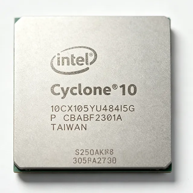
The Intel 10CX105YU484I5G is a Cyclone 10 GX field-programmable gate array (FPGA) offering 104,000 logic cells, 8,641,536 bits of embedded memory, and 188 user I/O resources in a 484-pin fine-pitch BGA package (designation U484), built on a 20 nm process with an industrial temperature-grade ordering designation (I5G). The device targets configurable digital logic, high-speed interface aggregation, and industrial embedded systems. As of 2026-09-05, XAIPART lists the part as active and in stock with 99,999 units available, MOQ 1, and pricing from $1,636.3636 at quantity 1 down to $954.5455 at 1,000 units. This guide covers verified specifications, design-in considerations, sourcing comparisons, and what buyers should watch next.
What Is the 10CX105YU484I5G and Why Does It Matter?
The 10CX105YU484I5G is a member of Intel's Cyclone 10 GX FPGA family. An FPGA is a semiconductor device whose digital logic and interconnects are configured after manufacturing, allowing a design team to implement changing logic functions, interface protocols, control algorithms, and signal-processing datapaths without committing to a fixed-function ASIC. The Cyclone 10 GX family combines programmable logic with I/O and embedded functional blocks, so a single device can consolidate functions that might otherwise require several connected components.
The verified specifications of this ordering part number are:
| Parameter | Verified Value |
|---|---|
| Manufacturer | Intel |
| Product Type | Field Programmable Gate Array (FPGA) |
| Family | Cyclone 10 GX |
| Logic Cells | 104,000 |
| Embedded Memory | 8,641,536 bits |
| User I/O | 188 |
| Package | 484-BFBGA (U484 designation) |
| Number of Pins | 484 (ball terminals) |
| Mounting Type | Surface Mount |
| Process Technology | 20 nm |
| Temperature Grade | Industrial |
| Lifecycle Status | Active |
The ordering code encodes two important attributes: the U484 package designation and the I5G suffix, which carries the industrial temperature grade and speed-grade identifier. Engineers should confirm the full temperature-range and qualification wording in the official Intel datasheet before final design sign-off. Note that the database records AEC-Q100 as not applicable, so this part should not be treated as automotive-qualified.
How Do You Select and Design In the 10CX105YU484I5G?
Choose the 10CX105YU484I5G when your design needs the verified 104,000-cell capacity, 188 user I/O resources, and a 484-pin BGA implementation for complex control, interface aggregation, or signal-processing functions. Simpler glue logic can often use a lower-density FPGA or CPLD, which simplifies routing, power, and cost. Once selected, follow this design sequence:
- Capacity and architecture fit: Map your state machines, protocol handlers, and datapaths against 104,000 logic cells and 8,641,536 bits of embedded memory. Usable capacity depends on synthesis results, so run your actual RTL early.
- I/O planning: Budget the 188 user I/O resources carefully. Usable I/O varies with voltage-bank configuration, transceiver assignments, configuration pins, and reserved interfaces. Verify all I/O-bank voltage constraints from the official documentation before pin assignment.
- PCB implementation: The 484-BFBGA package requires controlled-impedance routing, continuous power planes, careful BGA escape routing, a via-in-pad strategy, defined solder-mask openings, and decoupling capacitors placed close to supply pins. Signal-integrity analysis is important even if the design does not use every I/O.
- Power and configuration: Verify power sequencing, supply rails, clocking requirements, and the configuration architecture from Intel's recommended operating conditions. Exact capacitor values, allowed voltage rails, and clocking limits are not provided in the distributor data; use the official datasheet and reference designs rather than estimating them.
- Thermal design: Treat the device as a complex high-speed digital component. Obtain thermal resistance data and maximum power figures from Intel documentation; these values are not in the distributor listing and must not be estimated.
For schematic capture and footprint generation, obtain the official package drawing and complete pin table from Intel. The verified data confirms a 484-ball BGA with ball terminals but does not include the full ball map, ball dimensions, or recommended land pattern.
Where Does the 10CX105YU484I5G Deliver the Most Value in Real Systems?
The verified application profile spans industrial control, communications, test and measurement, video and image processing, data acquisition, and protocol bridging. Three representative scenarios:
- Industrial control and automation: The 104,000 logic cells and 188 user I/O resources provide headroom for sensor aggregation, deterministic state machines, timing control, and communication between machine modules, consolidating functions that would otherwise need several fixed-function components.
- Test and measurement: Configure counters, trigger logic, timing engines, calibration routines, and instrument-control interfaces in programmable hardware, updating measurement behavior without redesigning the instrument. The 188 I/O resources connect acquisition modules and peripherals.
- Embedded protocol bridge: Implement protocol parsing, frame assembly, clock-domain crossing, and supervisory control, adapting the bridge as endpoint protocols change during development. Validate latency, clock-domain behavior, and reset sequencing on hardware.
For video and image processing, the device can handle line buffers, pixel formatting, region-of-interest logic, and synchronization; however, DSP block count, supported video interface rates, and memory bandwidth are not stated in the distributor data and must be confirmed from Intel documentation before architecture commitment. Likewise, for communication equipment, the transceiver count, maximum data rate, and supported I/O standards require datasheet confirmation.
What Are the Alternatives and How Does 10CX105YU484I5G Compare?
No verified drop-in replacement for the 10CX105YU484I5G is established by the available cross-reference data. A true replacement must match the same package, pinout, I/O-bank behavior, configuration architecture, and key electrical characteristics. The comparison data identifies one related Cyclone 10 GX ordering variant:
| Parameter | 10CX105YU484I5G | 10CX105YF672E5G |
|---|---|---|
| Family | Cyclone 10 GX | Cyclone 10 GX |
| Package Designation | U484 (484-BFBGA) | F672 |
| Temperature Ordering Suffix | I (industrial designation per listing) | E (different ordering option) |
| Drop-in Compatible | — | No — different package, not verified pin-to-pin compatible |
Because the F672 variant uses a different package, it requires a new PCB footprint and possibly a system-design review. Do not substitute it without official compatibility confirmation from Intel. Other same-family or cross-brand parts should be treated as redesign candidates, not drop-in replacements, until the manufacturer confirms compatibility.
Regarding 10CX105YU484I5G versus 10CX105YU484E5G: both are U484 variants, but the available data does not quantify all electrical or timing differences between the I5G and E5G ordering suffixes. Validate the official Intel comparison before substituting one for the other.
What Is the Market Position, Lifecycle, and Supply Situation?
The lifecycle status of the 10CX105YU484I5G is recorded as active, based on its listing as a current ordering part number. No manufacturer longevity or discontinuation statement is included in the available data, so confirm the current lifecycle status with Intel or an authorized distributor for long-production programs.
On the supply side, as of 2026-09-05 XAIPART reports 99,999 units in stock with MOQ 1, which supports prototypes through volume builds. Verified tier pricing as of 2026-09-05:
| Quantity | Unit Price (USD) |
|---|---|
| 1+ | $1,636.3636 |
| 10+ | $1,181.8182 |
| 100+ | $1,045.4545 |
| 500+ | $1,000.00 |
| 1000+ | $954.5455 |
That is a 41.7% unit-price reduction from 1 unit to 1,000 units. Inventory is dynamic; refresh the quote immediately before purchase. Regulatory fields (RoHS, REACH, lead-free, halogen-free) are recorded as unknown in the database, so request current material-declaration documentation from Intel before making any regulatory compliance claim.
What Should Buyers and Engineers Watch Next?
Anchor your purchasing and design decisions to these verified facts:
- Price breaks are meaningful: At the 500-unit tier the price reaches $1,000.00 and at 1,000 units $954.5455 (as of 2026-09-05), so consolidating orders materially reduces unit cost for production programs.
- Speed-grade selection affects substitution: The I5G ordering code includes the speed-grade identifier 5; any redesign must confirm speed-grade, temperature-grade, and package equivalence through Intel's official ordering information.
- Documentation gaps to close: Before production approval, obtain the official datasheet and package drawing, then confirm supply voltages, I/O-bank restrictions, timing limits, transceiver capabilities, thermal data, and the complete pinout — none of these detailed values are in the distributor listing.
- Compliance documentation: RoHS and REACH status are unknown in the database; secure a current material declaration for your regulatory file.
- 20 nm platform context: The 20 nm process technology places this device in a high-density programmable-logic class. When evaluating future design reuse, compare against other Cyclone 10 GX members at the system level rather than assuming footprint compatibility across package designations.
For prototypes, the MOQ of 1 and immediate stock at XAIPART remove typical lead-time barriers. For production, lock in quantity pricing and confirm date-code requirements and allocation policies with your supplier at order time. The combination of 104,000 logic cells, 8,641,536 bits of embedded memory, 188 user I/O, and industrial temperature ordering makes the 10CX105YU484I5G a strong candidate for programmable industrial, test, and communication platforms — provided you validate all electrical and timing details against Intel's official documentation.
Comments
Be the first to comment.
🔐 Please sign in to post a comment.
Don't have an account? Sign up