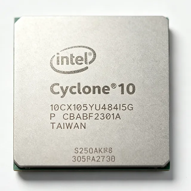
10CX105YU484I5G - 104K-Cell Cyclone 10 GX FPGA | Intel | Industrial Systems
MPN: 10CX105YU484I5G ✓ Active| Qty | Unit Price | Extended |
|---|---|---|
| 1 | $1636.3636 | $1,636.36 |
| 10 | $1181.8182 | $11,818.18 |
| 100 | $1045.4545 | $104,545.45 |
| 500 | $1000 | $500,000.00 |
| 1,000 | $954.5455 | $954,545.50 |
10CX105YU484I5G Overview
An FPGA is a semiconductor device whose digital logic and interconnects are configured after manufacturing. Its hierarchy is FPGA, programmable logic device, configurable logic integrated circuit, and digital semiconductor. Unlike a fixed-function ASIC, an FPGA can implement changing logic functions, interface protocols, control algorithms, and signal-processing datapaths. The Cyclone 10 GX family places programmable logic resources together with I/O and embedded functional blocks, allowing a system designer to consolidate functions that might otherwise require several connected components.
The defining feature of 10CX105YU484I5G is its 104,000-cell Cyclone 10 GX architecture. The device provides 188 user I/O resources, 8,640,? memory resources as reported by the distributor description, and 484 package terminals. Its FPGA structure supports configurable parallel logic, serial communication, state machines, timing logic, and custom control blocks. The exact supported transceiver count, maximum operating frequency, power supply limits, and embedded block details must be confirmed from the manufacturer datasheet before final design sign-off.
The 10CX105YU484I5G uses a 20 nm process technology, as identified in the distributor listing. This places the component in a high-density programmable-logic class aimed at designs that need more integration than a small CPLD or low-capacity FPGA. The package uses a 484-pin BGA footprint, so PCB escape routing, via-in-pad strategy, solder-mask definition, and signal-integrity analysis are important. The device should be treated as a complex high-speed digital component even where a particular design does not use every available I/O.
Typical applications include industrial control and automation, communication equipment, test and measurement, video and image processing, and custom data-acquisition systems. These applications benefit from the ability to revise logic, support multiple interface standards, and adapt timing or protocol behavior without replacing the entire PCB. The 188 I/O resources are especially relevant to systems that aggregate sensors, control signals, memory interfaces, and management buses.
When designing with this FPGA, verify all I/O-bank voltage constraints, clocking requirements, configuration architecture, power sequencing, and supported interface standards from the manufacturer documentation. The industrial-grade ordering code should be checked against the complete temperature and qualification wording in the official datasheet. This page combines verified distributor attributes, package and sourcing information, and practical engineering guidance; values not exposed by the supplied search data are explicitly marked rather than estimated.
Drop-in alternatives for 10CX105YU484I5G — same package, pin-to-pin compatible. Different-package parts requiring PCB rework are excluded.
Variants in this series
Same-series models that are drop-in compatible with 10CX105YU484I5G (same form factor and footprint) — differing in Package, RoHS Status, Embedded Memory, Mounting Type, Logic Elements.
Quick Comparison Tool — Select alternative parts for side-by-side comparison:
No drop-in alternatives available for this product.
Request Alternatives10CX105YU484I5G Maximum Ratings & Electrical Characteristics
| Manufacturer | Intel |
| Product Type | Field Programmable Gate Array (FPGA) |
| Family | Cyclone 10 GX |
| Logic Cells | 104000 |
| Embedded Memory | 8641536 bits |
| User I/O | 188 |
| Package | 484-BFBGA |
| Package Designation | U484 |
| Number of Pins | 484 |
| Terminal Form | Ball |
| Mounting Type | Surface Mount |
| Process Technology | 20 nm |
| Temperature Grade | Industrial |
| Orderable Part Number | 10CX105YU484I5G |
| RoHS Status | unknown |
| REACH Status | unknown |
| AEC-Q100 | not_applicable |
| Lead-Free Status | unknown |
| Halogen-Free Status | unknown |
10CX105YU484I5G u484 Pin Configuration Guide
Pin configuration for 10CX105YU484I5G (u484 package). This digital IC includes GPIO, communication interfaces (UART, SPI, I2C), and power pins. Refer to the manufacturer datasheet for alternate pin functions and configuration options. Essential for embedded system design and PCB layout.

No detailed pinout data available for 10CX105YU484I5G.
Refer to the datasheet for full pin configuration.
Typical Applications
10CX105YU484I5G is suitable for 6 applications: Industrial Control Systems, Communication Equipment, Test and Measurement Equipment, Video and Image Processing, Data Acquisition and Control, Embedded Protocol Bridge.
Industrial Control Systems
10CX105YU484I5G fits industrial control systems that require configurable logic for sensor aggregation, deterministic control, and communication between multiple machine modules. Its verified 104,000 logic cells and 188 user I/O resources provide headroom for state machines, protocol handling, timing control, and supervisory functions. The FPGA can consolidate functions that would otherwise require several fixed-function components. The industrial ordering designation is useful for equipment designs, but the complete temperature and qualification conditions must be confirmed from Intel documentation. PCB implementation should use the verified 484-BFBGA package, controlled impedance, and a power distribution network designed from the official recommended operating conditions. Because the supplied data does not provide I/O voltage limits, timing margins, or power figures, those values must not be estimated.
Recommended
Communication Equipment
10CX105YU484I5G is a potential fit for communication equipment requiring programmable data handling, protocol conversion, and flexible control around high-speed interfaces. The 104,000-cell architecture and 188 user I/O resources can support receive and transmit control logic, packet processing, error handling, and management functions. Its 484-pin BGA package accommodates many interface connections, but the supplied data does not state the number of transceivers, maximum data rate, or supported I/O standards. Those limitations must be checked in the official Cyclone 10 GX documentation before using the device in a communication product. The FPGA can reduce component count when several control functions must change during development. However, signal-integrity planning, reference-clock distribution, and I/O-bank placement must be based on verified electrical data rather than inferred values.
Recommended
Test and Measurement Equipment
10CX105YU484I5G can support test and measurement systems that need configurable measurement sequencing, signal conditioning control, and high-speed data capture coordination. The verified 104,000 logic cells allow implementation of counters, trigger logic, timing engines, calibration routines, and instrument-control interfaces, while 188 user I/O resources help connect acquisition modules and control peripherals. The FPGA is valuable when measurement behavior must be updated or customized without redesigning the entire instrument. The 484-BFBGA package requires careful via escape, impedance control, and thermal planning. The supplied data does not provide maximum clock frequency, supported I/O standards, or power consumption, so those values must be obtained from the official datasheet. Instrument designers should also validate configuration storage, reset behavior, clock jitter, and measurement timing margin in hardware.
Recommended
Video and Image Processing
10CX105YU484I5G may be used in video or image-processing equipment where pixel data, frame synchronization, and control logic must be handled in programmable hardware. The 104,000-cell device can be configured for line buffers, pixel formatting, region-of-interest logic, synchronization, and control of external image sensors or displays. Its 188 user I/O resources can aggregate sensor clocks, data buses, control signals, and downstream interfaces. The supplied data confirms the FPGA capacity and package but does not provide embedded memory resolution, DSP block count, clock limits, or supported video interface rates. Those details are essential for sizing pipelines and buffers. The 484-pin BGA implementation also requires a low-noise power and clock distribution strategy. Confirm all electrical limits, timing constraints, and external memory requirements from Intel's official documentation before architecture commitment.
Recommended
Data Acquisition and Control
10CX105YU484I5G is suitable for data-acquisition and control platforms that combine parallel sensor inputs, timing control, buffering, and communication processing. The verified 188 user I/O resources help connect multiplexers, converters, control signals, and management buses, while 104,000 logic cells provide capacity for sequencing, filtering, and protocol logic. The FPGA can be updated to support different acquisition rates or control algorithms, which is useful for modular equipment. The 484-BFBGA package gives access to many terminals but increases layout and manufacturing complexity. The supplied data does not specify I/O-bank voltage ranges, maximum toggle rates, memory bandwidth, or power dissipation. Engineers must use the official Cyclone 10 GX datasheet to calculate timing, thermal performance, decoupling, and interface compatibility rather than deriving those values from cell count.
Recommended
Embedded Protocol Bridge
10CX105YU484I5G can implement an embedded protocol bridge between industrial, communication, or test-system interfaces. The 104,000 logic cells can support protocol parsing, frame assembly, clock-domain crossing, and supervisory control, while the 188 user I/O resources provide connection capacity for multiple buses and sideband signals. A configurable bridge can adapt a system when endpoint protocols or timing requirements change during product development. The device is packaged in a 484-pin BGA, so the design must account for many simultaneous switching outputs and the resulting signal-integrity and power-delivery demands. The supplied web data does not establish supported I/O standards, transceiver count, maximum clock, or electrical limits. Verify those details in the official datasheet, then validate protocol latency, clock-domain behavior, error handling, and reset sequencing on hardware.
Recommended
Recommended Products Summary
Engineering reference data for 10CX105YU484I5G — comparison, design guidance, and compliance information.
Selection Guide
Comparison with Alternatives
| Parameter | This Product |
|---|---|
| Package | 484-BFBGA / U484 |
| Brand | Intel |
| Family | Cyclone 10 GX |
| Logic Cells | 104000 |
| User I/O | 188 |
| Number of Pins | 484 |
| Process Technology | 20 nm |
| Temperature Grade | Industrial designation |
| Drop-In Compatibility | No verified alternative identified |
Key Differentiators
- Verified 104,000-cell Cyclone 10 GX density (vs 10CX105YF672E5G)
- 484-pin U484 BGA implementation (vs 10CX105YF672E5G)
- Industrial ordering designation I5G (vs 10CX105YU484E5G)
- 188 user I/O resources (vs 10CX085YU484I5G)
Design Notes
Use the official 484-BFBGA package drawing and Intel reference design before generating the footprint. A 484-ball BGA requires controlled escape routing, correct via and solder-mask rules, and careful fanout for power, ground, clocks, and high-speed I/O. Do not infer land dimensions or ball numbering from the generic package name. Confirm the exact U484 package revision, pin map, and recommended footprint against the manufacturer documentation.
Create the power distribution network from the official operating-condition table, including permitted rail tolerances, current requirements, power-up sequencing, and decoupling recommendations. The supplied data confirms a 484-pin FPGA and 20 nm process, but does not provide voltage, current, or power values. Keep high-frequency decoupling close to the associated power pins and use plane-based distribution where the reference design permits. Validate rail sequencing and transient behavior on the finished board.
Plan I/O-bank placement and controlled-impedance routing before schematic release. The verified data gives 188 user I/O resources, but does not provide supported voltage levels, I/O standards, toggle rates, or transceiver limits. Assign clocks and high-speed interfaces to compliant locations, keep reference-clock routing short, provide appropriate return paths, and follow the official Cyclone 10 GX guidelines for terminations and differential pairs. Simulate or measure critical interfaces because package escape and simultaneous switching can affect margin.
Do not substitute a same-family or different-package FPGA without a complete engineering review. The supplied data identifies 10CX105YF672E5G as an F672 variant, which is not established as compatible with the U484 484-pin package. Similarly, E5G, I5G, and other ordering variants are not automatically drop-in equivalents. Confirm package, pinout, I/O-bank behavior, configuration method, timing, power, and qualification together. Treat any part sharing only the Cyclone 10 GX family name as a redesign candidate until Intel provides written compatibility evidence.
Compliance Information
The supplied data identifies an industrial temperature-grade designation, but does not provide a verified RoHS, REACH, lead-free, halogen-free, or conflict-minerals declaration. Automotive qualification is not established, so AEC-Q100 is recorded as not_applicable only because the provided data does not identify an automotive qualification.







