What Is the MSP430F5304IPTR and Why Should Engineers Choose It?
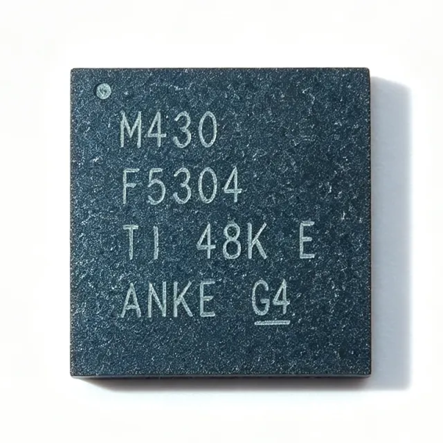
The Texas Instruments MSP430F5304IPTR is a 16-bit ultra-low-power mixed-signal microcontroller built on the MSP430 CPUXV2 core, running at up to 25 MHz with 8KB Flash memory (8K x 8), 6KB SRAM, and an integrated 3.3V LDO, packaged in a 48-pin LQFP (7x7 mm) surface-mount body rated from -40C to +85C (I grade). On-chip peripherals include four 16-bit timers, a 10-bit ADC, one USCI (UART/SPI/I2C), a 32-bit hardware multiplier, DMA, an RTC with alarm capabilities, and 31 I/O pins. The part is in active lifecycle status and available on XAIPART with 99,999 units in stock, MOQ 1, priced from $3.45 at qty 1 down to $2.10 at qty 1000+ as of 2026-09-02. For battery-powered metering, portable medical monitoring, industrial sensor nodes, and duty-cycled data loggers, it delivers a single-supply power tree, microamp-range standby behavior via five low-power modes, and a flexible clock system (VLO, REFO, XT1, DCO) that lets you trade clock accuracy against current consumption per application phase.
This guide consolidates everything a design engineer or buyer needs: verified specifications, design-in guidance, drop-in alternatives within the MSP430F530x subfamily, and sourcing details anchored to XAIPART's real product database. All values below come from the verified TI datasheet-backed data [verify against the official datasheet at https://www.ti.com/lit/gpn/msp430f5304].
How Do You Select and Design In the MSP430F5304IPTR?
Memory and Firmware Budgeting
The MSP430F5304 is the smallest memory configuration of the MSP430F530x subfamily, with 8KB Flash and 6KB SRAM. Budget your firmware before committing: if your control logic, scheduling code, and fixed-function metering firmware fit within 8KB, this is the lowest-cost option in the subfamily. TI designed the family for code portability - the MSP430F5xx/F6xx User's Guide (SLAU208) peripheral set is shared across family members, so code migrates freely. Verify Flash/SRAM sizing and package pinout before board reuse, because memory-density variants exist in identical footprints. If your code sits near the 8KB limit or you expect growth, the pin-compatible MSP430F5308 (16KB Flash) or MSP430F5309 (32KB Flash) drop into the same 48-pin LQFP without a board respin.
Power Architecture and Clock System
The integrated 3.3V LDO (PMM core voltage regulator) generates the regulated core voltage internally, so a single external rail powers the entire device - a major simplification versus MCUs needing dual rails. Decoupling per TI's datasheet layout guidance plus one supply rail covers the power section. The clock system offers five low-power modes (LPM0-LPM4.5) and sources the 25 MHz maximum clock from the internal DCO, with VLO, REFO, and XT1 crystal options. For duty-cycled designs, run the RTC from REFO or a crystal in standby, use the VLO for coarse wake-up timing, and rely on fast interrupt wake-up to keep average current in the microamp range. [VERIFY_NEEDED: exact per-mode current consumption figures - consult the datasheet electrical characteristics table.] Note that the verified database does not list the supply voltage range: [DATA_NEEDED: supply voltage range].
Peripherals and Signal Routing
The single USCI multiplexes UART, SPI, and I2C, so plan your serial topology carefully - if your system needs two independent serial links simultaneously (for example, UART to a host plus SPI to external Flash such as the W25Q64JVSSIG), choose the MSP430F5310, which provides two USCI modules. The 10-bit ADC with external channels such as A0 (pin 24) and A1 (pin 25) handles sensor and shunt inputs; pair it with DMA to move samples to SRAM without CPU intervention. Four 16-bit timers deliver PWM for fan or heater control and precise sampling intervals. The 32-bit hardware multiplier offloads energy-calculation and sensor-linearization arithmetic from the CPU.
Programming, Debug, and Toolchain
Development uses TI Code Composer Studio (CCS), the free Energia Arduino-compatible IDE, or IAR Embedded Workbench. Hardware debug goes through the standard Spy-Bi-Wire interface: pin 38 is TEST/SBWTCK (test mode / Spy-Bi-Wire clock) and pin 31 is RST/NMI (reset or non-maskable interrupt). TI LaunchPad boards and the MSP-FET programmer cover the whole MSP430F5xx family, protecting your tooling investment across future projects. Crystal circuits connect at pin 4 (PJ.0/XIN) and pin 5 (PJ.1/XOUT). Power enters through multiple digital supply pins, including pin 13 (DVCC1) and pin 48 (DVCC3), with grounds at pin 14 (DVSS1).
Package Selection
The IPTR suffix specifies the 48-pin LQFP (7x7 mm) package, industrial temperature range (-40C to +85C), and tape-and-reel packing. If your assembly house prefers tray packing, the MSP430F5304IPT offers the same package with trays. For denser boards, the MSP430F5304IRGZR is the same die in a 48-pin VQFN (7x7 mm) with a different footprint.
Which Alternatives Can Replace the MSP430F5304IPTR?
No true pin-to-pin cross-brand equivalent exists. Functionally comparable ultra-low-power MCUs include the NXP LPC1100 series and STMicroelectronics STM32L0 series, but these use different 32-bit Cortex-M0+ cores, pinouts, and toolchains, so a redesign - not a drop-in swap - is required. Within TI's own subfamily, these verified drop-in alternatives apply:
| Parameter | MSP430F5304IPTR | MSP430F5308IPTR | MSP430F5309IPTR | MSP430F5310IPTR | MSP430F5304IRGZR | MSP430F5304IPT |
|---|---|---|---|---|---|---|
| Core | MSP430 CPUXV2, 16-bit | Same core | Same core | Same core | Same die | Same die |
| Max Clock | 25 MHz | 25 MHz | 25 MHz | 25 MHz | 25 MHz | 25 MHz |
| Flash | 8KB | 16KB | 32KB | 32KB | 8KB | 8KB |
| SRAM | 6KB | [DATA_NEEDED: SRAM of F5308] | [DATA_NEEDED: SRAM of F5309] | 10KB | 6KB | 6KB |
| USCI | 1 | 1 | 1 | 2 | 1 | 1 |
| Package | 48-LQFP (7x7) | 48-LQFP/VQFN (pin-compatible) | 48-LQFP/VQFN (pin-compatible) | 48-pin footprint family | 48-VQFN (7x7) | 48-LQFP (7x7) |
| Drop-in? | Base part | Yes - same pinout | Yes - same pinout | Yes - footprint-compatible | No - different footprint | Yes - same package, tray packing |
Summary: the F5308 and F5309 are pure memory upgrades with identical peripherals and pinout; the F5310 adds SRAM and a second USCI in a footprint-compatible package; the IRGZR changes footprint only; the IPT changes packing only. [VERIFY_NEEDED: exact SRAM values for F5308 and F5309 before publishing the table.]
Where Does the MSP430F5304IPTR Fit in the Market and Supply Chain?
Lifecycle status is active per the verified database, and supply is healthy: XAIPART lists 99,999 units in stock with MOQ 1 as of 2026-09-02. Authorized distributors such as DigiKey and Mouser list the part as in stock and shipping today, with pricing approximately $2-$4 per unit depending on quantity as of 2026-08-30. On XAIPART specifically, tiered pricing as of 2026-09-02 is: $3.45 at qty 1, $3.10 at qty 10, $2.72 at qty 100, $2.38 at qty 500, and $2.10 at qty 1000 (tape and reel). [DATA_NEEDED: manufacturer lifecycle roadmap and long-term availability commitments beyond the active status flag.] Because TI actively sells pin-compatible density variants, one board layout can span a memory range - a supply-chain hedge worth encoding into your approved vendor list.
What Should Buyers Watch Going Forward?
First, anchor your BOM to the memory-fit decision: the F5304's 8KB Flash is sufficient for fixed-function metering and appliance firmware, but firmware growth trends argue for dual-sourcing the footprint with the 16KB F5308 as a pre-approved alternate. Second, the single USCI is the main architectural constraint - if your product roadmap adds a second serial link (network coprocessor plus local display, for example), qualify the two-USCI MSP430F5310 early since it is footprint-compatible. Third, the integrated 3.3V LDO keeps your power tree to one rail; any move to a competing Cortex-M0+ platform (LPC1100, STM32L0) costs you the pinout, the toolchain, and a board redesign, so stick with the subfamily for derivatives. Fourth, exploit the pricing curve: the step from $3.45 (qty 1) to $2.10 (qty 1000+) as of 2026-09-02 rewards consolidating annual volume into one tape-and-reel release. Finally, confirm the supply voltage range from the current TI datasheet before finalizing the power budget, since the verified database does not list it. With 25 MHz performance, DMA, a hardware multiplier, RTC standby timekeeping, and five low-power modes in a 7x7 mm package, the MSP430F5304IPTR remains a benchmark choice for ultra-low-power 16-bit designs.
Comments
Be the first to comment.
🔐 Please sign in to post a comment.
Don't have an account? Sign up