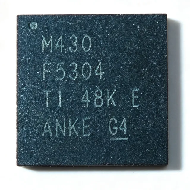
MSP430F5304IPTR - 16-bit 25MHz 8KB Flash MCU | Texas Instruments
MPN: MSP430F5304IPTR ✓ Active| Qty | Unit Price | Extended |
|---|---|---|
| 1 | $3.95 | $3.95 |
| 10 | $3.55 | $35.50 |
| 100 | $3.1 | $310.00 |
| 500 | $2.75 | $1,375.00 |
| 1,000 | $2.4 | $2,400.00 |
MSP430F5304IPTR Overview
An ultra-low-power microcontroller (MCU) is a single-chip processor optimized to minimize active and standby current draw, essential for battery-operated and energy-harvesting systems. The MSP430 family sits within the broader hierarchy of 16-bit microcontrollers -> mixed-signal MCUs -> embedded processors, and is widely recognized as an industry benchmark for low-power design.
Key features include the flexible clock system with five selectable low-power modes, a hardware 32x32 multiplier that offloads arithmetic from the CPU, and DMA for peripheral-to-memory transfers without CPU intervention. Active-mode consumption is approximately 195 uA/MHz at 8 MHz and 3V during Flash execution, with supply voltage supported from 2.4V to 3.6V.
The MSP430F5xx architecture pairs the von Neumann CPUXV2 core with a clock system supporting VLO, REFO, XT1, and DCO sources, allowing designers to trade clock accuracy against current consumption. Interrupt-driven operation with fast wake-up keeps average current in the microamp range in duty-cycled applications. The integrated LDO simplifies the power tree by generating the core supply from a single external rail.
Typical applications include battery-powered metering, portable medical monitoring, industrial sensor nodes, and consumer appliances where the combination of 25 MHz performance, one USCI serial port, and 31 GPIO covers most moderate-complexity control tasks.
Design consideration: the family shares the MSP430F5xx/F6xx User's Guide peripheral set, so code migrates freely between family members; verify Flash/SRAM sizing and package pinout before board reuse, as memory-density variants exist in identical 48-LQFP footprints.
This page synthesizes distributor pricing, drop-in alternatives, and practical design notes not found in the manufacturer datasheet, with data verified as of 2026-09-01.
Drop-in alternatives for MSP430F5304IPTR — same package, pin-to-pin compatible. Different-package parts requiring PCB rework are excluded.
Quick Comparison Tool — Select alternative parts for side-by-side comparison:
MSP430F5304IPTR
✓ In Stock
$2.1 / Unit
View Datasheet →MSP430F5308IPT
📋 Reference alternative (not in catalog)
MSP430F5308IPTR
📋 Reference alternative (not in catalog)
MSP430F5309IPTR
📋 Reference alternative (not in catalog)
MSP430F5310IPTR
📋 Reference alternative (not in catalog)
MSP430F5304IPTR Maximum Ratings & Electrical Characteristics
| Core | MSP430 CPUXV2 16-bit RISC |
| Max Clock Frequency | 25 MHz |
| Flash Memory | 8 KB (8K x 8) |
| SRAM | 6 KB (6K x 8) |
| Supply Voltage Range | 2.4 V to 3.6 V |
| Active Mode Current | 195 uA/MHz at 8 MHz, 3 V, Flash execution |
| ADC Resolution | 10-bit |
| Timers | 4 x 16-bit |
| Serial Interfaces | 1 x USCI (UART/SPI/I2C) |
| I/O Pins | 31 |
| DMA | Yes |
| Hardware Multiplier | 32x32 hardware multiplier |
| RTC | RTC with alarm capabilities |
| Integrated LDO | 3.3 V core LDO |
| Oscillator Type | Internal (VLO, REFO, DCO; XT1 external) |
| Low-Power Modes | 5 modes (LPM0-LPM4) |
| Operating Temperature Range | -40C to +85C (Industrial, I suffix) |
| Package | 48-LQFP (PT), 7x7 mm |
| Mounting Type | Surface Mount |
| Packaging | Tape & Reel (TR) |
| Lifecycle Status | Active |
MSP430F5304IPTR 48-lqfp (pt), 7x7 mm Pin Configuration Guide
Pin configuration for MSP430F5304IPTR (48-lqfp (pt), 7x7 mm package). This digital IC includes GPIO, communication interfaces (UART, SPI, I2C), and power pins. Refer to the manufacturer datasheet for alternate pin functions and configuration options. Essential for embedded system design and PCB layout.

No detailed pinout data available for MSP430F5304IPTR.
Refer to the datasheet for full pin configuration.
Typical Applications
MSP430F5304IPTR is suitable for 6 applications: Battery-Powered Metering, Portable Medical Monitoring, Industrial Sensor Nodes, Consumer Appliances, Energy Harvesting Systems, Handheld Test and Measurement Instruments.
Battery-Powered Metering
The MSP430F5304IPTR fits utility and sub-metering products where a 10-year battery life target dominates the design. Its 195 uA/MHz active current at 8 MHz and 3V, plus LPM3 standby operation with the RTC keeping time, allow duty-cycled sampling loops with microamp average current. The 10-bit ADC reads analog front ends from shunt or divider networks, while the 32x32 hardware multiplier accelerates energy-accumulation math (V x I integration) without long software multiply loops. The integrated 3.3V core LDO permits a single-cell or regulated 3V rail without an external regulator, saving board area and quiescent budget. One USCI covers an M-Bus, UART, or I2C communication port to the meter's optical or wireless head, and the 8KB Flash holds a compact metering state machine with room for calibration tables.
Recommended
Portable Medical Monitoring
In portable medical devices such as pulse oximeters, glucose meters, and wearable vital-sign monitors, the MSP430F5304IPTR's ultra-low-power profile extends battery life while the 25 MHz CPUXV2 core executes signal-processing routines such as digital filtering on sampled analog channels. The 10-bit ADC acquires sensor front-end outputs, and DMA moves samples into the 6KB SRAM without CPU intervention, letting the core sleep between conversion bursts to minimize average current. Fast interrupt wake-up from low-power modes supports event-driven sampling triggered by the RTC alarm, a key pattern in medical duty-cycling. The 31 GPIO pins drive displays, LEDs, and buzzers directly, while the single USCI provides I2C or SPI links to pressure, optical, or temperature sensors. Industrial -40C to +85C temperature rating supports clinical and ambulatory environments alike.
Recommended
Industrial Sensor Nodes
Industrial sensor nodes for condition monitoring, environmental logging, and process supervision benefit from the MSP430F5304IPTR's balance of analog integration and low standby power. The device's five low-power modes allow the node to sleep between measurement intervals, waking on RTC alarm or external interrupt to sample the 10-bit ADC, timestamp readings, and transmit over a UART or I2C link via the USCI. The VLO and REFO clock sources provide low-accuracy-but-low-power timing when crystal precision is unnecessary, reducing BOM cost. Its industrial -40C to +85C operating range and 2.4V to 3.6V supply tolerance accommodate battery end-of-life droop and unregulated supply rails common in field installations. The 8KB Flash accommodates Modbus-fragment or proprietary protocol code, and identical-footprint F5308/F5309/F5310 variants provide a growth path if the node later adds FFT-based vibration analytics.
Recommended
Consumer Appliances
White goods, small appliances, thermostats, and chargers use the MSP430F5304IPTR as a low-cost control MCU where touch/button interfaces, temperature sensing, and simple actuator drive suffice. The 31 GPIO directly drive relays, LEDs, and seven-segment or LCD-less indicator arrangements, while the 10-bit ADC reads NTC thermistors and user potentiometers. The hardware multiplier speeds PID loop computations for temperature or motor-speed control at modest code size, well within the 8KB Flash budget. The internal DCO and VLO oscillators eliminate external crystals in applications where timing accuracy is non-critical, cutting BOM cost and layout complexity. The single USCI implements UART-based factory test ports or I2C links to display drivers and EEPROM. Active status and multi-source availability (DigiKey, Mouser) make it safe for long-life appliance production programs.
Recommended
Energy Harvesting Systems
Energy-harvesting designs powered by thermoelectric, photovoltaic, or RF scavenging demand electronics that operate from microwatt budgets and irregular supply rails - a natural fit for the MSP430F5304IPTR. Its 2.4V minimum supply and integrated core LDO tolerate the slowly rising or sagging rails typical of harvested energy storage, while VLO-based clocking allows execution at the lowest possible active current during brief wake windows. The architecture's five low-power modes and fast wake-up let the system spend most of its time in LPM3 with the RTC running, accumulating energy between tasks. Sensor reads via the 10-bit ADC and data bursts over the USCI are scheduled around available energy, and the 8KB Flash stores compact protocol stacks. Supercapacitor or thin-film-battery supervision can be implemented with ADC channels and comparator-free software thresholds.
Recommended
Handheld Test and Measurement Instruments
Battery-powered handheld instruments such as cable testers, environmental meters, and portable calibrators leverage the MSP430F5304IPTR's combination of analog acquisition, arithmetic acceleration, and long standby life. The 10-bit ADC samples measurement front ends; the 32x32 hardware multiplier and DMA enable fast averaging, RMS computation, and calibration math in the 6KB SRAM buffer space. The RTC with alarm provides timestamping for logged readings, and LPM3 standby between user interactions yields months of shelf life on primary cells - a decisive purchasing criterion for handheld tools. The USCI supports UART links to printers or Bluetooth/USB bridge modules, while multiple GPIO handle keypad scanning and indicator multiplexing. Designers can start on the 8KB F5304 and migrate to pin-identical F5308/F5309/F5310 parts if analysis firmware outgrows the memory budget without any PCB change.
Recommended
Recommended Products Summary
Engineering reference data for MSP430F5304IPTR — comparison, design guidance, and compliance information.
Selection Guide
Comparison with Alternatives
| Parameter | This Product | MSP430F5308IPT | MSP430F5309IPTR | MSP430F5310IPTR | MSP430F5304IPT |
|---|---|---|---|---|---|
| Package | 48-LQFP (PT), 7x7 mm | 48-LQFP (PT) - same | 48-LQFP (PT) - same | 48-LQFP (PT) - same | 48-LQFP (PT) - same |
| Brand | Texas Instruments | Texas Instruments | Texas Instruments | Texas Instruments | Texas Instruments |
| Flash Memory | 8 KB | 16 KB | 24 KB | 32 KB | 8 KB |
| SRAM | 6 KB | 6 KB | 6 KB | 6 KB | 6 KB |
| Max Clock Frequency | 25 MHz | 25 MHz | 25 MHz | 25 MHz | 25 MHz |
| Supply Voltage | 2.4 V to 3.6 V | 2.4 V to 3.6 V | 2.4 V to 3.6 V | 2.4 V to 3.6 V | 2.4 V to 3.6 V |
| Packaging | Tape & Reel (TR) | Tube/Tray | Tape & Reel | Tape & Reel | Tube/Tray |
| Lifecycle Status | Active | Active | Active | Active | Active |
Key Differentiators
- Lowest Flash density and cost in the pin-identical family (vs MSP430F5308IPT)
- Integrated 3.3V core LDO simplifies the power tree (vs MSP430F5309IPTR)
- Same-footprint growth path up to 32KB (vs MSP430F5310IPTR)
- Hardware 32x32 multiplier on a low-cost 16-bit core (vs MSP430G2553IPW28R)
Design Notes
The MSP430F5304 integrates a core LDO that generates the CPU core supply from the single 2.4V-3.6V external rail. Decouple the LDO output (VCORE) with the exact capacitance specified in the TI family datasheet - typically a 470 nF class capacitor on VCORE plus bulk capacitance on DVCC. Do not load VCORE externally or use it to power other circuitry; doing so destabilizes the regulator and can cause brownout resets under load transients.
On the 48-LQFP (7x7 mm) footprint, place 100 nF ceramic decoupling capacitors within 2 mm of each VCC/VSS pin pair, and provide a solid ground pour on the layer beneath the device. Route the JTAG/Spy-Bi-Wire pins (TCK, TMS/TDI, TDO/TDI) to a standard 14-pin JTAG or 4-wire SBW header even if debugging is done once - rework on fine-pitch LQFP to add these traces later is error-prone. Keep the XT1 crystal (if used) traces short and guarded with ground.
Verify Flash sizing before code freeze: 8KB on the F5304 fills quickly with protocol stacks and calibration tables, while pin-identical F5308/F5309/F5310 variants offer 16-32KB. Also confirm USCI count - the F5304 provides one USCI, so designs needing simultaneous SPI and UART require either software serial or migration within the family. Finally, respect the BSL and bootloader pin states at reset (floating P1.1/P1.3-class pins) to prevent unintended bootloader entry in the field.
Estimated: in a duty-cycled sensor node sampling once per second, active work of 5 ms at 25 MHz costs roughly 195 uA/MHz x 25 MHz x 0.005 = 24.4 uA average contribution alone; the remainder of the budget is set by LPM3 current and RTC. Clock the CPU at the lowest frequency that meets latency deadlines, because active energy scales with both frequency and time - overshooting to 25 MHz for a task that fits at 8 MHz multiplies dynamic energy without shortening wake windows.
Compliance Information
digchip packaging data lists a GREEN plastic package with industrial operating range; per-part material declarations should be confirmed on TI.com.







