The Micron Technology MT53E512M32D1ZW-046 is a 16Gbit Mobile LPDDR4 SDRAM organized as 512M x 32, operating at up to 2133 MT/s (2.133 GHz clock, 3.5 ns cycle time) from a 1.06 V to 1.17 V core supply. It is housed in a 200-ball TFBGA package measuring 10 x 14.5 mm, rated for -25C to +85C (WT grade), and it is an active, RoHS-compliant catalog part. On the XAIPART MT53E512M32D1ZW-046 product page the part is in stock with 99999 units available, MOQ 1, and volume pricing from $113.30 per unit at 1,000+ pieces down to $141.63 for single units as of 2026-10-13. A single package delivers roughly 8.5 GB/s of peak bandwidth on its 32-bit bus, which makes it a fit for smartphone main memory, automotive infotainment prototypes, industrial HMI panels, networking line-card buffers, and edge AI accelerators. This guide covers verified specifications, design-in practice, drop-in grade variants, sourcing, and what to watch when buying LPDDR4 in 2025-2026.
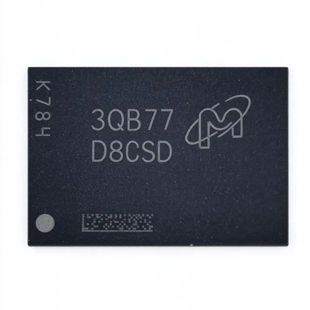
What Is the MT53E512M32D1ZW-046 and Which Specs Matter Most?
The MT53E512M32D1ZW-046 is Micron's 16Gbit (512M x 32) Mobile LPDDR4 SDRAM in the -046 speed bin. Mobile LPDDR4 SDRAM is a low-power double-data-rate synchronous DRAM optimized for battery-powered and thermally constrained systems. It belongs to the DRAM family alongside DDR4 and LPDDR4X, distinguished by its low core voltage, deep power-down modes, and per-bank or all-bank refresh architectures that cut idle power.
Every spec in the table below comes from the XAIPART verified product database:
| Parameter | Value |
|---|---|
| Memory Type | Mobile LPDDR4 SDRAM |
| Density | 16 Gbit |
| Organization | 512M x 32 |
| Data Rate | 2133 MT/s (2.133 GHz clock) |
| Cycle Time | 3.5 ns |
| Core Supply Range | 1.06 V to 1.17 V (1.106 V nominal) |
| Package | 200-TFBGA (10 x 14.5 mm) |
| Terminal Count | 200 |
| Operating Temperature | -25C to +85C (WT grade) |
| Mounting | Surface Mount |
| Built-in Temperature Sensor | Yes |
| Auto Precharge / Write Leveling / ZQ Calibration / Async Reset / Data Mask | All supported |
| Automotive Qualification | No (WT grade; AEC-Q100 variants exist as AIT:B / AUT:B) |
| RoHS | Compliant |
Architecturally, the device uses an 8n-prefetch pipeline with bank groups to deliver 2.133 Gb/s/pin while keeping standby and deep-power-down currents low. Dynamic voltage and frequency scaling with DVFS-compatible I/O termination lets you trade bandwidth against power in real time.
Takeaway: If your SoC has a 32-bit LPDDR4 controller and supports the -046 speed bin, this single die delivers full bus width, 2 GB of memory, and about 8.5 GB/s peak bandwidth in one 10 x 14.5 mm package.
How Do You Design In the MT53E512M32D1ZW-046 Successfully?
Controller and speed-bin check. LPDDR4 requires per-device training of read/write leveling and DQS oscillation at every boot. Confirm your SoC memory controller (NXP i.MX, Rockchip, and Qualcomm embedded families are typical x32 hosts) explicitly supports the -046 speed bin at 2133 MT/s. Training parameters are device-specific, so keep the memory within your SoC vendor's certified reference layout to guarantee training convergence at 2133 MT/s.
Power rails. The core supply range is 1.06 V to 1.17 V with 1.106 V nominal. Power the device from a stable 1.1 V-class rail with proper sequencing control, and use a separate I/O rail per your platform's power tree. Consult the official Micron datasheet for exact rail definitions and the I/O supply range; the authoritative AC/DC timing parameters for the -046 bin live only in that document, downloadable from Micron's part-detail page or via the Farnell-hosted PDF at farnell.com/datasheets/3919393.pdf.
Layout. Mount the 200-TFBGA on a multi-layer PCB with all ground balls connected to a solid ground plane through via-in-pad or short dog-bone escapes. LPDDR4 fly-by routing requires length-matched command/address nets and carefully controlled 40-ohm-class single-ended impedance on DQ/DQS nets. Place the package close to the SoC. Re-run write leveling and DQS training after any layout change - the data mask function and on-die termination settings also depend on calibrated impedance from ZQ calibration.
Thermal and power budgeting. At 2133 MT/s with typical LPDDR4 activity factors, budget roughly 0.5-1 W package power (estimate; verify with Micron's power calculator for your workload). Use the built-in temperature sensor to adapt self-refresh timing, and derate junction temperature with thermal vias under the TFBGA-200 thermal balls in 24/7 industrial systems.
Boot sequencing. The asynchronous reset function supports fast, deterministic boot - important in cluster and networking designs that need watchdog-initiated recovery or hot-swap behavior.
Takeaway: Treat LPDDR4 design-in as a controller-plus-layout exercise: verify -046 bin support, hold the 1.106 V-class core rail, follow fly-by length-matched routing, and budget training time in your boot flow.
What Bandwidth and Buffering Can You Actually Get From One Package?
Do the arithmetic before you commit to a memory architecture:
- Peak bandwidth per package: 2133 MT/s x 32 bits = 8.532 Gb/s-per-pin aggregate translates to approximately 8.5 GB/s peak per package on the 32-bit bus - enough for multitasking mobile OS workloads, graphics compositing plus protocol stacks, or quantized CNN inference on an NPU-equipped SoC.
- Two-package scaling: Two devices give 4 GB of buffering with roughly 17 GB/s aggregate - the configuration used on dense networking line cards and edge AI modules.
- Cycle time headroom: The 3.5 ns cycle time sustains burst-heavy queue-management traffic; the data mask function enables partial writes for header manipulation without full cache-line writes.
- Record depth for instruments: 16Gbit per package yields deep waveform-capture record lengths in a small footprint on dense mainboards.
Takeaway: For most 32-bit-controller designs, one MT53E512M32D1ZW-046 covers 2 GB / 8.5 GB/s needs; plan two packages when buffering or inference bandwidth doubles.
Which MT53E512M32D1ZW-046 Variants Are Drop-In Alternatives?
Because Micron builds WT:B, IT:B, and automotive grades from the same 16Gbit die in the identical 200-TFBGA (10 x 14.5 mm) footprint, grade swaps are pin-to-pin compatible. Cross-brand substitutes are not.
| Variant | Key Difference vs WT:B | Best For |
|---|---|---|
| MT53E512M32D1ZW-046 IT:B | Industrial temperature -40C to +95C (vs -25C to +85C WT) | Instruments and industrial systems specified below -25C |
| MT53E512M32D1ZW-046 IT:B TR | Identical die and industrial spec, tape-and-reel delivery | High-volume automated assembly |
| MT53E512M32D1ZW-046 AIT:B | LPDDR4X grade, AEC-Q100 qualified (per Arrow listing), same 16Gbit 512M x 32 2133 MT/s die and package | Automotive infotainment, cluster, ADAS memory |
| MT53E512M32D1ZW-046 AUT:B | LPDDR4X automotive grade per DigiKey, AEC-Q100, same density/organization/package | Automotive programs requiring the AUT build |
| MT53E512M32D1ZW-046 AAT:B | Alternate automotive qualification/build of the same die, same package and speed bin | Automotive builds specifying the AAT grade |
Cross-brand substitution warning: A Samsung or SK Hynix 16Gb x32 LPDDR4 part can match density, organization, and speed on paper, but LPDDR4 ball maps differ between vendors and firmware memory training parameters are device-specific. There is no guaranteed pin-for-pin cross between vendors. Treat any cross-brand swap as a redesign requiring schematic, layout, and controller-training validation. Per DigiKey's cross-reference tool, parametric equivalents exist reliably only within this Micron family.
LPDDR4X note: The AIT:B and AUT:B variants are LPDDR4X, which reduces I/O voltage versus LPDDR4 for lower power. LPDDR4X is generally backward-compatible at the controller level if the SoC supports it - confirm your controller's LPDDR4X support and I/O voltage rails before substituting.
Takeaway: Stay inside the MT53E512M32D1ZW-046 family for drop-in swaps; choose IT:B for cold environments, AIT:B/AUT:B (AEC-Q100, LPDDR4X) for automotive, and never assume cross-brand pin compatibility.
Where Should You Use This Part - and Where Should You Not?
Verified application fit from the XAIPART product database:
| Application | Why It Fits | Critical Spec Used |
|---|---|---|
| Smartphone / tablet main memory | 16Gbit in one x32 die eliminates chip stacking on narrow controllers; ~8.5 GB/s peak sustains multitasking mobile OS workloads | 16 Gbit, 512M x 32, 2133 MT/s, 1.106 V core |
| Automotive infotainment and cluster | AEC-Q100 AIT:B/AUT:B variants only; async reset enables deterministic boot | AEC-Q100 (variants), asynchronous reset = Yes |
| Industrial HMI and edge panels | WT grade covers most factory-floor ambients; ZQ calibration holds signal integrity on long PCB runs | -25C to +85C, ZQ calibration = Yes |
| Networking line cards | Two packages reach 4 GB buffering; data mask enables efficient partial writes | 16 Gbit, 3.5 ns cycle, data mask = Yes |
| Edge AI inference accelerators | ~8.5 GB/s per package, ~17 GB/s with two; low core voltage suits battery platforms | 2133 MT/s x32, 1.106 V nominal |
| Test and measurement | Fast x32 capture path; ZQ calibration holds output impedance accuracy across temperature swings | 2133 MT/s, ZQ calibration = Yes |
Where not to use the WT:B: Any environment below -25C or above +85C, and any automotive program requiring AEC-Q100 qualification. Select the IT:B or an automotive grade variant instead - the die and footprint are identical, so this is a sourcing decision, not a redesign.
Takeaway: Match the grade to the ambient, not the application label: WT:B for consumer/industrial-wide, IT:B for -40C systems, AIT:B/AUT:B for qualified automotive.
What Is the Market and Supply Position of the MT53E512M32D1ZW-046?
The part is an active Micron catalog part, verified in the XAIPART database as of 2026-10-13. XAIPART shows 99999 units in stock, MOQ 1, with tiered pricing: $141.63 (qty 1+), $134.55 (10+), $127.47 (100+), $120.39 (500+), and $113.30 (1000+) as of 2026-10-13. For context on distribution pricing, LCSC listed the WT:B from $141.63 single-unit with 96 units in stock as of 2026-09-02, and DigiKey and Newark indicated ships-today availability at that date; the IT:B TR variant was listed around $249.63 on DigiKey AU, reflecting the premium for the wider industrial temperature envelope.
Authorized sources include DigiKey, Mouser, Newark, LCSC, Avnet, and Arrow. LPDDR4 demand fluctuates with mobile market cycles, so confirm real-time stock before scheduling production - lead times for factory orders typically range from stock to several weeks. For volume quotes and lead times, request pricing directly on the XAIPART product page or browse the full component catalog.
Takeaway: Supply is currently healthy (active lifecycle, five-figure stock, MOQ 1), but mobile-cycle volatility argues for locking volume pricing early - the step from $141.63 to $113.30 at 1,000 pieces is a 20% saving.
What Should LPDDR4 Buyers Watch in 2025-2026?
1. Grade availability tracks automotive demand. The same 16Gbit die serves consumer (WT:B), industrial (IT:B), and AEC-Q100 automotive (AIT:B/AUT:B) programs. When automotive allocation tightens, consumer-grade lead times often follow; keep the pin-compatible grade variants on your approved-vendor list so you can pivot without a respin.
2. LPDDR4X migration pressure. Micron's automotive variants of this exact die are LPDDR4X, which lowers I/O voltage for reduced power. New SoC platforms increasingly design around LPDDR4X-class I/O rails, so qualify your controller for LPDDR4X now to preserve a path to the AIT:B/AUT:B grades.
3. Bandwidth-driven density pairing. At 2133 MT/s, one package delivers ~8.5 GB/s and two deliver 4 GB at ~17 GB/s aggregate. Designs that need more bandwidth per chip-select will drive demand for stacked or higher-speed bins, so pin your -046 speed-bin support in controller firmware and keep training scripts versioned per die revision.
4. Price-tier discipline. With verified tiers stepping from $141.63 down to $113.30 at 1,000 units as of 2026-10-13, consolidating buys across projects into 500- or 1,000-piece lots captures $14-$28 per unit. Always request volume quotes; distribution list prices (like the ~$249.63 IT:B TR listing) can diverge sharply from contract pricing.
5. Training and validation workload. Every layout change or die revision requires re-running write leveling and DQS training at boot. Standardize on the SoC vendor's certified reference layout and document your training results per board build to cut qualification cycles when you swap between WT:B, IT:B, and automotive grades of this same die.
Takeaway: The hardware risk here is low because all grades share one footprint; the sourcing risk is timing. Anchor your BOM to this active Micron catalog part, secure 1,000-piece pricing early, and keep LPDDR4X-capable controllers in your roadmap. For more component-level sourcing analysis, see the XAIPART Blog.
Comments
Be the first to comment.
🔐 Please sign in to post a comment.
Don't have an account? Sign up