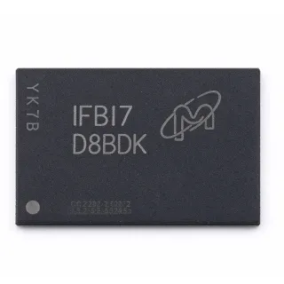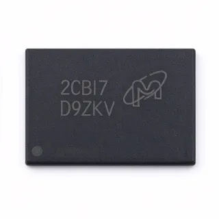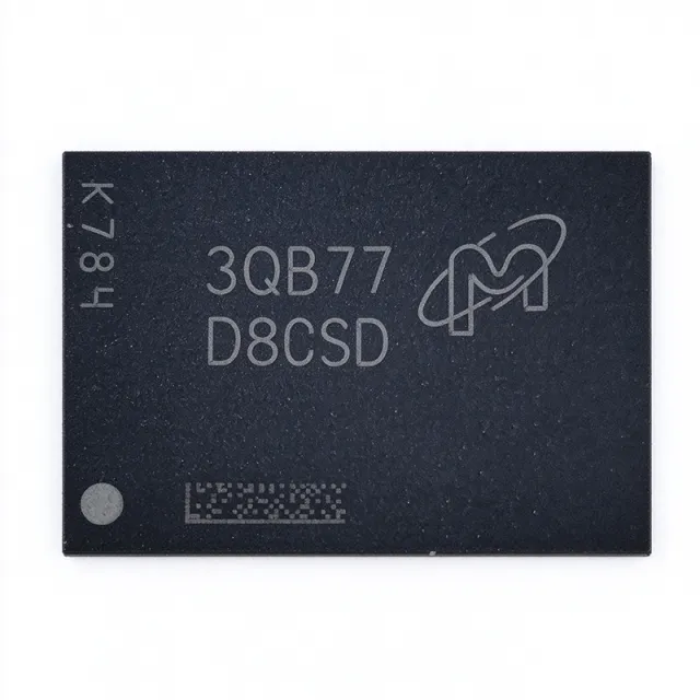
MT53E512M32D1ZW-046 - 16Gbit LPDDR4 SDRAM TFBGA-200 | Micron
MPN: MT53E512M32D1ZW-046 ✓ Active| Qty | Unit Price | Extended |
|---|---|---|
| 1 | $141.63 | $141.63 |
| 10 | $134.55 | $1,345.50 |
| 100 | $127.47 | $12,747.00 |
| 500 | $120.39 | $60,195.00 |
| 1,000 | $113.3 | $113,300.00 |
MT53E512M32D1ZW-046 Overview
Mobile LPDDR4 SDRAM is a low-power double-data-rate synchronous dynamic random-access memory optimized for battery-powered and thermally constrained systems. Within the memory hierarchy, it belongs to the DRAM family alongside DDR4 and LPDDR4X, distinguished by a 1.106 V nominal core voltage, deep power-down modes, and per-bank or all-bank refresh architectures that reduce idle power in smartphones, tablets, and embedded controllers.
Key features include a wide x32 data bus for maximum bandwidth per chip-select, a built-in temperature sensor that drives self-refresh timing, auto precharge, write leveling, ZQ calibration, asynchronous reset, and data mask functions. The WT temperature grade covers -25C to +85C operation, while the D1 die provides 16Gbit of density in a single monolithic circuit.
Architecturally, the device uses an 8n-prefetch pipeline with bank groups, delivering 2.133 Gb/s/pin data rates while maintaining low standby and deep-power-down currents. Dynamic voltage and frequency scaling, together with DVFS-compatible I/O termination, allows system designers to trade bandwidth against power in real time, which is essential for mobile SoC platforms and automotive infotainment stacks.
Typical applications include smartphone and tablet main memory, automotive infotainment and ADAS SoC memory, industrial HMI panels, and networking equipment line-card buffers. The x32 organization suits SoCs with 32-bit memory controllers such as NXP i.MX, Rockchip, and Qualcomm embedded families.
Design consideration: LPDDR4 requires per-device training of read/write leveling and DQS oscillation at every boot; ensure the SoC memory controller supports the -046 speed bin and that layout maintains length-matched, on-termination-capable fly-by routing.
This page synthesizes distributor pricing, grade-level drop-in variants, and practical design notes not found in the manufacturer datasheet.
Drop-in alternatives for MT53E512M32D1ZW-046 — same package, pin-to-pin compatible. Different-package parts requiring PCB rework are excluded.
Quick Comparison Tool — Select alternative parts for side-by-side comparison:
MT53E512M32D1ZW-046 IT:B
📋 Reference alternative (not in catalog)
MT53E512M32D1ZW-046 AIT:B
📋 Reference alternative (not in catalog)
MT53E512M32D1ZW-046 AUT:B
📋 Reference alternative (not in catalog)
MT53E512M32D1ZW-046 AAT:B
📋 Reference alternative (not in catalog)
MT53E512M32D1ZW-046 IT:B TR
📋 Reference alternative (not in catalog)
MT53E512M32D1ZW-046 Maximum Ratings & Electrical Characteristics
| Memory Type | Mobile LPDDR4 SDRAM |
| Density | 16 Gbit |
| Organization | 512M x 32 |
| Clock Frequency | 2.133 GHz (data rate 2133 MT/s) |
| Cycle Time | 3.5 ns |
| Core Supply Voltage Range | 1.06 V to 1.17 V |
| Package | 200-TFBGA (10 x 14.5 mm) |
| Terminal Count | 200 |
| Operating Temperature | -25C to +85C |
| Mounting Type | Surface Mount |
| Built-in Temperature Sensor | Yes |
| Auto Precharge | Yes |
| Write Leveling | Yes |
| ZQ Calibration | Yes |
| Asynchronous Reset | Yes |
| Data Mask Function | Yes |
| Automotive Qualification | No (WT grade; AEC-Q100 variants available as AIT:B / AUT:B) |
| RoHS Status | Compliant |
MT53E512M32D1ZW-046 200-tfbga (10 x 14.5 mm) Pin Configuration Guide
Pin configuration for MT53E512M32D1ZW-046 (200-tfbga (10 x 14.5 mm) package). This digital IC includes GPIO, communication interfaces (UART, SPI, I2C), and power pins. Refer to the manufacturer datasheet for alternate pin functions and configuration options. Essential for embedded system design and PCB layout.

No detailed pinout data available for MT53E512M32D1ZW-046.
Refer to the datasheet for full pin configuration.
Typical Applications
MT53E512M32D1ZW-046 is suitable for 6 applications: Smartphone and Tablet Main Memory, Automotive Infotainment and Cluster, Industrial HMI and Edge Computing Panels, Networking Equipment Line Cards, AI Edge Inference Accelerators, Test and Measurement Instrumentation.
Smartphone and Tablet Main Memory
The MT53E512M32D1ZW-046 targets mobile flagship memory subsystems where its 16Gbit density in a single x32 die eliminates chip stacking on narrow controllers. At 2133 MT/s on a 32-bit bus it delivers approximately 8.5 GB/s peak bandwidth per package, sufficient for application processors running multitasking mobile OS workloads. The 1.106 V core voltage and deep power-down modes minimize standby drain, which is critical for battery life; the built-in temperature sensor automatically adjusts self-refresh timing across -25C to +85C. Place the TFBGA-200 close to the SoC with length-matched DQ/DQS fly-by routing and use DVFS to trade bandwidth against power dynamically during use.
Recommended
Automotive Infotainment and Cluster
Automotive head units and digital clusters require high-bandwidth DRAM that survives extended temperature and vibration environments. The AEC-Q100-qualified AIT:B and AUT:B variants of the MT53E512M32D1ZW-046 die provide the identical 16Gbit, 512M x 32, 2133 MT/s footprint for such designs, while the WT:B suits non-qualified prototype builds. The x32 organization pairs naturally with 32-bit memory controllers in automotive SoCs, and the asynchronous reset function supports the fast, deterministic boot sequencing that cluster designs mandate. Designers should power the device from a stable 1.1 V rail with sequencing control and validate memory training across the full automotive temperature range on the target board.
Recommended
Industrial HMI and Edge Computing Panels
Industrial human-machine interface panels and edge gateways run Linux-class SoCs that need 2 GB-class DRAM with low idle power. The MT53E512M32D1ZW-046's -25C to +85C WT grade covers most factory-floor ambient conditions, and its ZQ calibration maintains signal integrity despite long PCB runs to remote display modules. The 2133 MT/s speed bin sustains 8.5 GB/s per package on a 32-bit bus, enough for graphics compositing and protocol stacks simultaneously. Because industrial systems often run 24/7, use the built-in temperature sensor to modulate self-refresh rate and derate junction temperature through thermal vias under the TFBGA-200 thermal balls.
Recommended
Networking Equipment Line Cards
Switch, router, and 5G small-cell line cards use LPDDR4 as deep-packet buffering and control-plane memory. The MT53E512M32D1ZW-046 offers 16Gbit per package with a wide x32 bus, letting designers reach 4 GB of buffering with two devices while conserving board area on dense cards. The 3.5 ns cycle time and 2133 MT/s data rate sustain the burst-heavy traffic patterns of queue management, and the data mask function enables efficient partial writes for header manipulation. Networking designs should budget termination power on the address/command fly-by network and exploit the asynchronous reset for hot-swap and watchdog-initiated recovery sequences.
Recommended
AI Edge Inference Accelerators
Edge AI modules running vision and audio inference need memory bandwidth close to the accelerator. The MT53E512M32D1ZW-046 supplies approximately 8.5 GB/s of peak bandwidth per package on its 32-bit LPDDR4 interface, and two packages reach 4 GB with about 17 GB/s aggregate - adequate for quantized CNN inference on NPU-equipped SoCs. Its low 1.106 V core and self-refresh modes fit battery-powered camera and drone platforms operating from -25C to +85C. Write leveling and DQS training must be re-executed after any layout change; keep the memory within the SoC vendor's certified reference layout to guarantee training convergence at 2133 MT/s.
Recommended
Test and Measurement Instrumentation
Bench instruments, logic analyzers, and portable oscilloscopes use high-bandwidth DRAM for waveform capture and post-processing buffers. The MT53E512M32D1ZW-046's 2133 MT/s, x32 interface moves acquisition data quickly into capture memory, while 16Gbit per package yields deep record lengths in a small footprint on dense mainboards. The ZQ calibration function maintains output impedance accuracy despite instrument internal temperature swings, and the data mask function supports efficient acquisition-header updates without full cache-line writes. Choose the IT:B grade for instruments specified to -40C, and route DQ/DQS as length-matched fly-by groups with on-die-termination-aware simulation before tape-out.
Recommended
Recommended Products Summary
Engineering reference data for MT53E512M32D1ZW-046 — comparison, design guidance, and compliance information.
Selection Guide
Comparison with Alternatives
| Parameter | This Product | MT53E512M32D1ZW-046 IT | MT53E512M32D1ZW-046 AIT | MT53E512M32D1ZW-046 AUT | MT53E512M32D1ZW-046 AAT |
|---|---|---|---|---|---|
| Package | 200-TFBGA (10 x 14.5 mm) | B: 200-TFBGA (10 x 14.5 mm) - same | B: 200-TFBGA (10 x 14.5 mm) - same | B: 200-TFBGA (10 x 14.5 mm) - same | B: 200-TFBGA (10 x 14.5 mm) - same |
| Brand | Micron Technology | B: Micron Technology | B: Micron Technology | B: Micron Technology | B: Micron Technology |
| Memory Type | Mobile LPDDR4 | B: Mobile LPDDR4 | B: Mobile LPDDR4X | B: Mobile LPDDR4X | B: Mobile LPDDR4 |
| Density / Organization | 16 Gbit / 512M x 32 | B: 16 Gbit / 512M x 32 | B: 16 Gbit / 512M x 32 | B: 16 Gbit / 512M x 32 | B: 16 Gbit / 512M x 32 |
| Speed | 2133 MT/s (2.133 GHz, 3.5 ns) | B: 2133 MT/s (2.133 GHz, 3.5 ns) | B: 2133 MT/s (2.133 GHz, 3.5 ns) | B: 2133 MT/s (2.133 GHz, 3.5 ns) | B: 2133 MT/s (2.133 GHz, 3.5 ns) |
| Operating Temperature | -25C to +85C (WT) | B: -40C to +95C (IT) | B: Automotive range (AIT) | B: Automotive range (AUT) | B: Automotive range (AAT) |
| Automotive AEC-Q100 | No | B: No | B: Yes (per Arrow listing) | B: Yes | B: Yes (automotive grade) |
Key Differentiators
- Industrial temperature range at identical footprint (vs MT53E512M32D1ZW-046 IT:B)
- Automotive upgrade without redesign (vs MT53E512M32D1ZW-046 AIT:B)
- Single-die x32 organization maximizes bandwidth per package (vs x16-organized 16Gbit competitors)
Design Notes
LPDDR4 fly-by topology is mandatory for command/address/clock nets: route CA[5:0], RAS-n, CAS-n, WE-n, CK_t/CK_c and CKE from the SoC through each DRAM with stub-free daisy chaining, terminating at the last device. DQ/DQS/DM nets are point-to-point per device and must be length-matched within the SoC vendor's tolerance (typically +-25 mil intra-byte). Keep the TFBGA-200 within the vendor-certified reference layout; deviations can cause read/write leveling training failures at 2133 MT/s.
The device requires separate VDD (core, 1.06-1.17 V) and VDD2 rails plus VDDQ for I/O; use dedicated LDO or buck outputs with soft-start sequencing per the Micron datasheet power-ramp requirements. Decouple each rail with bulk 10 uF plus per-ball 0.1 uF ceramics placed inside the package footprint. Estimated: at 2133 MT/s with a moderate activity factor, package power is roughly 0.5-1 W - run Micron's LPDDR4 power calculator with your actual traffic profile for budget verification.
Connect the ground/thermal balls of the 200-TFBGA to a solid internal ground plane with an array of vias under the package to spread heat into inner layers. Use the built-in temperature sensor output via the controller to adapt self-refresh timing rather than hard-coding worst-case values; this reduces idle power significantly in battery-operated designs. For automotive or sealed enclosures, verify junction temperature at maximum ambient plus worst-case workload and confirm the -046 speed bin derating requirements from the datasheet.
Do not assume cross-vendor substitution: LPDDR4 ball maps differ between Micron, Samsung, and SK Hynix, and memory training firmware is die-specific, as cross-reference sources note there is no guaranteed pin-for-pin cross. Also, the AIT:B/AUT:B variants are LPDDR4X - confirm controller compatibility with the reduced VDDQ before substituting on an LPDDR4-only board. Finally, verify the temperature grade letter (WT vs IT vs AIT/AUT) on the actual package marking when sourcing from brokers to avoid consumer parts in industrial builds.
Compliance Information
WT:B grade is not AEC-Q100 qualified; use AIT:B or AUT:B variants for automotive. RoHS/lead-free status inferred from catalog RoHS-compliant listing; REACH and halogen-free status not stated in provided data.