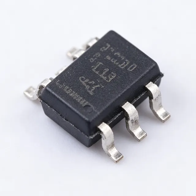
What Is the SN74AHC1G08-Q1 and Why Should Engineers Care?
The Texas Instruments SN74AHC1G08-Q1 (orderable part number SN74AHC1G08QDCKRQ1) is an automotive-qualified single 2-input positive-AND gate that performs the Boolean function Y = A AND B in positive logic. It operates from a 2V to 5.5V supply, delivers a maximum propagation delay of 9 ns at 5V, and comes in a 5-pin SC-70 (DCK) surface-mount package. The device carries AEC-Q100 (Q1) automotive qualification, RoHS compliance, and latch-up performance exceeding 250 mA per JESD 17, with ESD protection beyond 2000V HBM, 200V MM, and 1000V CDM per the TI datasheet. As of 2026-09-04, XAIPART lists it active and in stock with 99,999 units available, MOQ 1, priced at $0.32 for single units and $0.09 at 1,000 pieces. For engineers, the value proposition is simple: one fast, robust AND gate in a 2.0 mm × 1.25 mm footprint you can place exactly where gating is needed — a body-controller connector, a cluster strobe line, or a CAN node's transceiver enable — instead of routing traces to a large multi-gate device. You can check live stock and buy the SN74AHC1G08QDCKRQ1 on XAIPART.
How Does the SN74AHC1G08-Q1 Work? (Technical Guide to Selecting and Designing In This Logic IC)
The SN74AHC1G08-Q1 belongs to TI's AHC logic family, which uses a balanced CMOS architecture for low static power consumption. The unbuffered single-stage design keeps propagation delay tight and predictable across the operating range, and the output stage is push-pull CMOS with TTL-compatible levels and balanced drive. Inputs are standard CMOS type.
Key verified specifications
| Parameter | Value (verified) |
|---|---|
| Logic function | 2-input positive-AND gate (Y = A AND B) |
| Number of gates | 1 (single gate) |
| Supply voltage range | 2 V to 5.5 V |
| Max propagation delay | 9 ns at 5 V |
| Logic family | AHC |
| Automotive qualification | AEC-Q100 (Q1) |
| Latch-up performance | Exceeds 250 mA per JESD 17 |
| ESD protection | >2000 V HBM, >200 V MM, >1000 V CDM |
| Input / output type | Standard CMOS input, push-pull CMOS output |
| Package / mounting | SC-70-5 (DCK), surface mount |
| RoHS status | Compliant |
Pinout in SC-70-5
Per the TI datasheet, the SC-70 (DCK) pinout is: pin 1 = input A, pin 2 = GND, pin 3 = input B, pin 4 = output Y, pin 5 = VCC. The compact 2.0 mm × 1.25 mm footprint lets you place the single gate directly at the point of use.
Design-in best practices
First, respect the 2V–5.5V supply window: power the gate from whichever rail — 3.3V or 5V — its output must swing, since the push-pull output drives full rail at its own VCC. Second, because inputs are standard CMOS (not Schmitt-trigger), drive them with clean, fast edges; for slow or noisy signals, consider a Schmitt-input alternative (see the comparison below). Third, tie unused input pins to VCC or GND — with only two inputs on one gate this is trivial, but it matters during layout rework. Fourth, place a 0.1 µF decoupling capacitor close to the VCC pin to ensure clean switching edges and minimize ground bounce, especially in automotive noise environments. Fifth, treat the 9 ns propagation delay as a worst-case budget item: actual delay varies with supply voltage and load capacitance, decreasing at higher VCC and smaller loads.
Worked design example: gating an MCU chip-select with a power-good signal
Suppose a 3.3V MCU must have its chip-select gated by a 5V-domain power-good signal. Wire the chip-select to input A, the power-good output to input B, and VCC (pin 5) to the 5V rail. With a 9 ns maximum propagation delay at 5V, the gate adds effectively zero latency compared with any MCU chip-select timing budget, and the full-rail 5V push-pull output cleanly satisfies a 5V-side enable input. Add 0.1 µF of local decoupling at pin 5, and the design is complete — no pull resistors needed because the push-pull CMOS output drives actively in both states.
What Are the Best Alternatives and Drop-In Replacements for the SN74AHC1G08-Q1?
Based on verified database data, these are the alternatives to consider, each traded off against footprint and qualification requirements:
| Part | Grade | Package / Footprint | Key Difference vs SN74AHC1G08QDCKRQ1 | Drop-In? |
|---|---|---|---|---|
| SN74AHC1G08DCKR | Standard industrial (not AEC-Q100) | SC-70-5 (DCK) | Same die and pinout, standard grade | Yes — drop-in for non-automotive builds |
| SN74AHC1G08QDBVRQ1 | Automotive (AEC-Q100) | SOT-23-5 | Same die and function, different footprint | No — PCB footprint change required |
| 74AHC1G08GV,125 (Nexperia) | Cross-brand | SOT-353 / SC-88A (same as SC-70-5) | Pin-compatible; inputs overvoltage tolerant | Yes — same footprint and pinout |
| 74AHC1G08SE-7 | Cross-brand | SOT-25 | Single 2-input AND gate; verify pinout ordering | Verify pinout before use |
| SN74HCS08QDYYRQ1 | Automotive-equivalent function | SOT-23-5 | Adds Schmitt-trigger inputs | No — footprint change required |
Selection guidance from the verified FAQ data: choose the standard-grade SN74AHC1G08 for cost-sensitive industrial builds; choose the Nexperia 74AHC1G08GV,125 for cross-brand second sourcing on the same footprint (and select Nexperia's 74AHC1G08-Q100 for automotive builds to maintain qualification); choose SN74HCS08-Q1 when slow or noisy input edges need Schmitt-trigger hysteresis; choose LVC-family parts such as SN74LVC1G08 when faster propagation delay (around 3–4 ns at 3.3V) and lower dynamic power at high toggle rates matter more than the wide 2V–5.5V supply window.
What Is the Market Position, Lifecycle, and Supply Situation for This Part?
The SN74AHC1G08QDCKRQ1 is listed as active in the XAIPART product database. Supply is deep: 99,999 units in stock as of 2026-09-04, with MOQ 1 and tiered pricing of $0.32 (qty ≥1), $0.26 (qty ≥10), $0.16 (qty ≥100), $0.12 (qty ≥500), and $0.09 (qty ≥1000). Distributor data referenced in the verified FAQ also lists availability at DigiKey, Mouser, and TI.com with volume breaks below $0.10 at 1,000 pieces as of 2026-08-29. Lifecycle forecasts, obsolescence risk ratings, and multi-year supply commitments are not provided in the current database: [DATA_NEEDED: lifecycle forecast and PCN/obsolescence status]. For sourcing strategy, browse XAIPART's Logic ICs category for comparable single-gate logic inventory.
What Trends and Design Shifts Should Buyers Watch for Single-Gate Automotive Logic?
Buyers anchored to the verified data should watch four things. First, the shift toward distributed single-gate placement: the SC-70-5 footprint (2.0 mm × 1.25 mm) exists precisely because modern automotive PCBs place one gate at the signal source — connector-side conditioning, transceiver enable pins, power-path gating — rather than routing to centralized quad-gate devices. Second, dual-rail consolidation: the 2V to 5.5V supply range lets one SKU serve both 3.3V MCU-side and 5V field-side domains on the same board, which simplifies BOM management. Third, robustness as a baseline: AEC-Q100 qualification plus latch-up beyond 250 mA per JESD 17 and ESD above 2000V HBM are now table stakes for in-vehicle logic, which is why the -Q1 variant commands the design slot over standard-grade equivalents in automotive programs. Fourth, price stability at volume: at $0.09 per unit at 1,000 pieces as of 2026-09-04, this gate is effectively a commodity, so procurement risk lies in qualification continuity, not cost. When evaluating replacements, always confirm both footprint and pinout — as the alternatives table shows, functionally identical parts can differ in package (SOT-23-5 vs SC-70-5) or pin ordering (74AHC1G08SE-7 requires pinout verification). Read our related logic IC selection guide for a broader framework.
Comments
Be the first to comment.
🔐 Please sign in to post a comment.
Don't have an account? Sign up