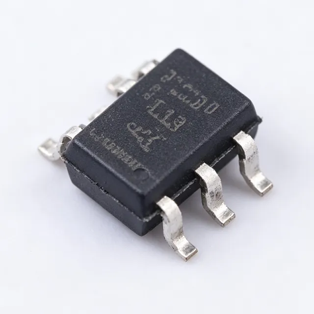
SN74AHC1G08-Q1 - Automotive 2-Input AND Gate SC-70-5 | TI
MPN: SN74AHC1G08QDCKRQ1 ✓ Active| Qty | Unit Price | Extended |
|---|---|---|
| 1 | $0.32 | $0.32 |
| 10 | $0.26 | $2.60 |
| 100 | $0.16 | $16.00 |
| 500 | $0.12 | $60.00 |
| 1,000 | $0.09 | $90.00 |
SN74AHC1G08QDCKRQ1 Overview
A single-gate logic IC integrates exactly one logic function - here an AND gate - in a tiny footprint, unlike traditional quad-gate devices such as the 74HC08. Single-gate devices sit within the broader CMOS logic IC family, under combinational logic, and are widely used for glue logic, signal gating, and enable generation in modern PCBs where board space is at a premium.
Key features include the AHC family's balanced CMOS architecture for low static power consumption, a wide 2V to 5.5V operating range supporting both 3.3V and 5V systems, and latch-up performance exceeding 250 mA per JESD 17. ESD protection exceeds 2000-V Human-Body Model, 200-V Machine Model, and 1000-V Charged-Device Model per TI datasheet. The -Q1 suffix denotes AEC-Q100 qualification for automotive applications.
The AHC technology provides TTL-compatible CMOS outputs with balanced drive and fast switching, while the unbuffered single-stage design keeps propagation delay tight and predictable across the operating range. Typical applications include automotive body electronics and cluster gating, industrial PLC I/O conditioning, and general-purpose enable/signal gating in mixed 3.3V/5V systems.
Design tip: keep unused input pins tied to VCC or GND, and place a 0.1uF decoupling capacitor close to the VCC pin to ensure clean switching edges and minimize ground bounce in automotive noise environments.
Drop-in alternatives for SN74AHC1G08QDCKRQ1 — same package, pin-to-pin compatible. Different-package parts requiring PCB rework are excluded.
Variants in this series
Same-series models that are drop-in compatible with SN74AHC1G08QDCKRQ1 (same form factor and footprint) — differing in Logic Family, Logic Function, Output Type, Package, Supply Voltage Range.
Quick Comparison Tool — Select alternative parts for side-by-side comparison:
SN74AHC1G08DCKR
📋 Reference alternative (not in catalog)
SN74AHC1G08QDBVRQ1
📋 Reference alternative (not in catalog)
74AHC1G08GV,125
📋 Reference alternative (not in catalog)
74AHC1G08SE-7
✓ In Stock
$0.09 / Unit
View Datasheet →SN74HCS08QDYYRQ1
📋 Reference alternative (not in catalog)
SN74AHC1G08QDCKRQ1 Maximum Ratings & Electrical Characteristics
| Logic Function | 2-Input Positive-AND Gate (Y = A AND B) |
| Number of Gates | 1 (single gate) |
| Supply Voltage Range | 2 V to 5.5 V |
| Max Propagation Delay | 9 ns at 5 V |
| Logic Family | AHC |
| Automotive Qualification | AEC-Q100 (Q1) |
| Latch-Up Performance | Exceeds 250 mA per JESD 17 |
| ESD Protection (HBM) | Exceeds 2000 V |
| ESD Protection (MM) | Exceeds 200 V |
| ESD Protection (CDM) | Exceeds 1000 V |
| Input Type | Standard CMOS |
| Output Type | Push-Pull CMOS |
| Package | SC-70-5 (DCK) |
| Mounting Type | Surface Mount |
| RoHS Status | Compliant |
SN74AHC1G08QDCKRQ1 Pin Configuration
| Pin 1 | A — Input A |
| Pin 2 | GND — Ground |
| Pin 3 | B — Input B |
| Pin 4 | Y — Output (Y = A AND B) |
| Pin 5 | VCC — Power supply, 2V to 5.5V |
Typical Applications
SN74AHC1G08QDCKRQ1 is suitable for 6 applications: Automotive Body Electronics, Instrument Cluster Signal Gating, Industrial PLC I/O Conditioning, Mixed-Voltage Glue Logic, CAN and Communication Node Enable Logic, Battery-Managed Power System Gating.
Automotive Body Electronics
The SN74AHC1G08-Q1 gates switch inputs, door status signals, and interlock conditions in body control modules, where its AEC-Q100 qualification and latch-up performance exceeding 250 mA per JESD 17 address automotive robustness requirements. Its 2V to 5.5V supply range tolerates automotive 5V rail variation, and the 9 ns propagation delay at 5V adds negligible timing skew. The SC-70-5 package fits dense body-controller PCBs, allowing a single gate to be placed directly at the connector-side conditioning circuit rather than routing long traces to a multi-gate device.
Recommended
Instrument Cluster Signal Gating
In instrument clusters, the device combines warning enable signals and backlight interlocks with a 9 ns maximum delay at 5V, keeping timing deterministic across the cluster MCU's strobe schedule. AEC-Q100 qualification covers the extended automotive temperature environment behind the dashboard. Operating from the 5V cluster rail with balanced AHC CMOS drive, its push-pull output can directly drive indicator buffer inputs or LED driver enable pins. Low static power consumption keeps quiescent draw negligible in partially powered cluster states, supporting key-off battery drain budgets in modern vehicles.
Recommended
Industrial PLC I/O Conditioning
The SN74AHC1G08-Q1 combines interlock and safety-enable signals in PLC digital input modules, where the 2V to 5.5V range supports both 3.3V MCU-side and 5V field-side rails on one board. The 9 ns propagation delay at 5V is far faster than PLC scan cycles, adding effectively zero latency to interlock chains. ESD protection exceeding 2000V HBM provides margin near field wiring, and the compact SC-70-5 package allows gating directly at terminal-block conditioning circuits. Standard CMOS inputs suit buffered, conditioned field signals from optocoupler outputs.
Recommended
Mixed-Voltage Glue Logic
The wide 2V to 5.5V supply window makes the SN74AHC1G08-Q1 a natural glue-logic element between 3.3V and 5V domains, for example gating a 3.3V MCU chip-select with a 5V-domain power-good signal. Balanced AHC CMOS output drive provides full-rail swing at the supply it is powered from, and the single-gate format eliminates unused-gate inputs that multi-gate packages create. Place the gate at the domain boundary with local 0.1uF decoupling to keep switching edges clean and limit ground bounce between domains.
Recommended
CAN and Communication Node Enable Logic
The device gates transceiver STB/EN pins with MCU wake signals in CAN and LIN nodes: its 9 ns delay ensures the transceiver mode transition happens within microseconds of the MCU decision, and AEC-Q100 qualification meets automotive network node requirements. SC-70-5 sizing lets the gate sit beside the TCAN-family transceiver on a dense node PCB. Low power consumption in standby supports the node's sleep-current budget, and the robust ESD ratings (over 2000V HBM) add margin in harsh in-vehicle EMC environments near connector routing.
Recommended
Battery-Managed Power System Gating
In battery management and power-path circuits, the SN74AHC1G08-Q1 combines power-good outputs and charger fault flags into a single system-enable signal. Its push-pull CMOS output directly drives load-switch enable pins without external pull resistors, and the 2V to 5.5V range matches both battery-backed 3.3V supervision rails and 5V power rails. The gate's fast 9 ns response prevents glitched enables during fault sequencing. Pair with a supervisor or PMIC power-good output, and tie the gate VCC to the always-on rail so the enable stays defined through power transitions.
Recommended
Recommended Products Summary
Engineering reference data for SN74AHC1G08QDCKRQ1 — comparison, design guidance, and compliance information.
Selection Guide
Comparison with Alternatives
| Parameter | This Product | SN74AHC1G08DCKR | 74AHC1G08GV,125 | 74AHC1G08SE-7 | SN74AHC1G08QDBVRQ1 |
|---|---|---|---|---|---|
| Package | SC-70-5 (DCK) | SC-70-5 (DCK) - same | SOT-353/SC-88A - same footprint | SOT-25 - same footprint | SOT-23-5 (DBV) - different footprint |
| Brand | Texas Instruments | Texas Instruments | Nexperia | Diodes Incorporated | Texas Instruments |
| Supply Voltage Range | 2 V to 5.5 V | 2 V to 5.5 V | 2 V to 5.5 V | 2 V to 5.5 V | 2 V to 5.5 V |
| Logic Function | 2-input AND | 2-input AND | 2-input AND | 2-input AND | 2-input AND |
| Automotive Grade (AEC-Q100) | Yes (Q1) | No | No (standard grade) | No | Yes (Q1) |
Key Differentiators
- AEC-Q100 automotive qualification (vs SN74AHC1G08DCKR)
- Smallest footprint with same die as DBV option (vs SN74AHC1G08QDBVRQ1)
- Wide 2V to 5.5V range versus fast LVC alternatives (vs 74AHC1G08GV,125)
Design Notes
Place a 0.1uF ceramic decoupling capacitor within 2-3 mm of the VCC pin (pin 5) and route a short return to GND (pin 2). Although a single AND gate draws little dynamic current, fast output edges into capacitive loads cause supply transients that, without local decoupling, couple into neighboring analog circuitry on shared rails.
This is a standard CMOS input device - do not leave inputs A or B floating, as unterminated CMOS inputs float near threshold and cause oscillation and excess ICC. Tie unused conditions to VCC or GND. Do not drive inputs from slow RC ramps; use a Schmitt-trigger buffer such as SN74LVC1G17 if edges are noisy or slow.
Power dissipation is dominated by output load switching, not static CMOS current. With a 50 pF load toggling at low frequencies, dissipation (P = C*V^2*f) stays in the microwatt range at 5V, so no thermal management is needed in the SC-70-5 package. Only high-frequency clock gating above tens of MHz merits a dissipation check.
Compliance Information
AEC-Q100 qualified (Q1 suffix) per TI product page. RoHS compliant and lead-free per distributor listings.






