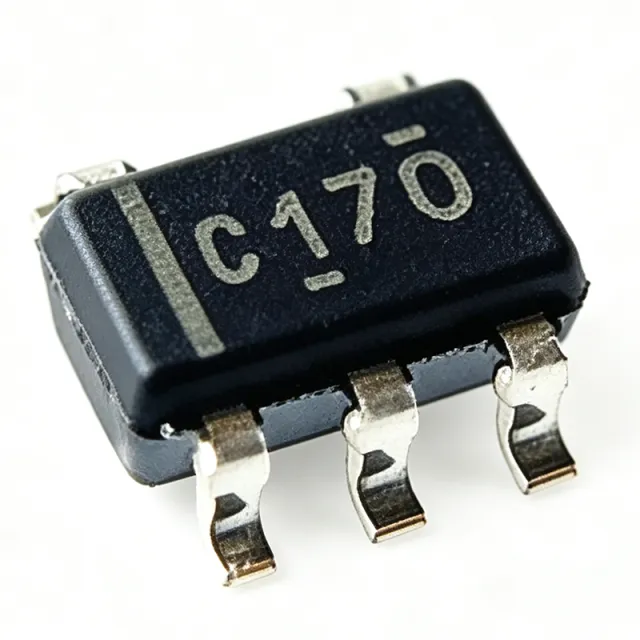
The SN74LVC1G17QDBVRQ1 is a Texas Instruments automotive-qualified (AEC-Q100) single Schmitt-trigger buffer that performs Y = A from a 1.65V to 5.5V supply in a 5-pin SOT-23 (DBV) surface-mount package. It operates across -40C to +125C, uses TI's CMOS LVC logic family with a push-pull output, and is RoHS/Pb-free with Green (Br/Sb-free) status. Unlike a standard buffer, its input hysteresis converts slow or noisy edges from RC networks, sensors, and long automotive harnesses into a single clean output transition. The part is active in lifecycle status, stocked at 99,999 units on XAIPART with MOQ 1, priced at $0.09 per unit at 1,000 pieces as of 2026-09-04. That combination - wide supply range, Schmitt input, automotive grade, and sub-$0.30 single-unit pricing - makes it one of the most practical single-gate signal-conditioning buffers available today for ECU, battery-management, industrial, and infotainment designs.
Quick Answers: What Should Every Buyer and Engineer Know First?
Before diving into the full technical guide, here are the fastest answers to the most common questions about the SN74LVC1G17QDBVRQ1.
What is it? A single non-inverting Schmitt-trigger buffer (Boolean function Y = A) in TI's LVC CMOS family, built for automotive and industrial signal conditioning. Its defining feature versus a plain buffer is input hysteresis: rising and falling thresholds differ, so slow or noisy inputs never cause output chatter.
What are its key verified specs? Supply range 1.65V to 5.5V; one channel with Schmitt-trigger input; push-pull output; -40C to +125C operating temperature; AEC-Q100 (Q1) qualification; SOT-23-5 (DBV) package, 5 pins, surface mount; Tape and Reel (DBVR) packaging. Propagation delay at a specified VCC is [DATA_NEEDED: propagation delay at specified VCC] and the output drive current rating is [DATA_NEEDED: IOL/IOH rating]; consult the TI datasheet for these switching and drive tables.
What does it cost and is it available? XAIPART tier pricing as of 2026-09-04: $0.28 at qty 1, $0.23 at 10, $0.15 at 100, $0.11 at 500, and $0.09 at 1,000+. Stock stands at 99,999 units with MOQ 1, and the part carries an active lifecycle status, so no lead-time risk is currently reported.
What is the pinout? Per the TI datasheet: pin 1 = A (Schmitt-trigger input), pin 2 = GND, pin 3 = Y (push-pull output), pin 4 = NC, pin 5 = VCC.
Technical Guide: How Do You Select, Design In, and Use This Schmitt-Trigger Buffer?
Why choose a Schmitt buffer instead of a standard buffer? Standard CMOS inputs require fast input edges; slow ramps (from RC filters, sensor outputs, optocouplers, or long cables) can cause multiple output transitions or oscillation. The SN74LVC1G17QDBVRQ1's Schmitt input sets distinct rising and falling trip points, guaranteeing one clean edge per event. This is the defining advantage over the SN74LVC1G34 standard buffer, which shares the same SOT-23-5 footprint and pinout but lacks hysteresis.
Step 1 - Match the supply domain. The 1.65V to 5.5V VCC range means one part number covers 1.8V, 2.5V, 3.3V, and 5V logic systems without level-shifting circuitry. In mixed-domain automotive modules, place the buffer near the connector or domain boundary and power it from the rail of the receiving logic.
Step 2 - Design the input network deliberately. Use the hysteresis as a design tool. For switch debouncing, connect the switch through an RC network - for example 10 kOhm and 100 nF, giving roughly a 1 ms time constant - into pin 1. The slow RC ramp crosses both Schmitt thresholds cleanly, and the push-pull output at pin 3 delivers exactly one debounced edge to the MCU GPIO. For RC oscillator squaring, feed the capacitor node directly to the input; operating at the 5.5V maximum maximizes hysteresis margin in noisy environments, while at 1.8V the part squares signals for low-voltage logic.
Step 3 - Support power integrity. Keep a 100 nF ceramic decoupling capacitor close to the VCC pin (pin 5) to maintain signal integrity, especially when the output drives fanout at high speed. The CMOS LVC architecture keeps static power dissipation low across the full supply range, which suits always-on automotive ignition-sense and keep-alive circuits.
Step 4 - Confirm automotive quality documentation. The Q1 suffix confirms AEC-Q100 qualification for automotive applications with -40C to +125C operation. TI's controlled-baseline approach - one assembly site, one test site, one fabrication site - supports automotive quality requirements such as PPAP documentation through TI. If your program requires PPAP, source the Q1 part specifically rather than the commercial SN74LVC1G17DBVR.
Step 5 - Handle assembly correctly. The DBVR suffix denotes SOT-23-5 tape and reel. The 5-pin DBV footprint is compact enough for dense board areas around connectors and flex-cable interfaces. Pin 4 is no-connect; leave it floating per the footprint.
Design caution on propagation delay: the verified database lists propagation delay as [DATA_NEEDED: propagation delay at specified VCC]; the digchip summary in the product description notes a typical value around 10.7 ns at low supply. For timing-critical paths, verify the exact per-VCC delay and Schmitt thresholds in the TI SN74LVC1G17-Q1 datasheet (Rev. A) before sign-off.
Which Packages and Pinout Does the SN74LVC1G17QDBVRQ1 Use?
The device ships in the 5-pin SOT-23 (DBV) surface-mount package. The functionally key pins are:
| Pin | Name | Function |
|---|---|---|
| 1 | A | Schmitt-trigger input |
| 2 | GND | Ground |
| 3 | Y | Push-pull buffer output (Y = A) |
| 4 | NC | No connect |
| 5 | VCC | Supply, 1.65V to 5.5V |
The same die is also offered in other packages (SC70, SM8, etc.) under different ordering part numbers, but the DBVR suffix specifically denotes SOT-23-5 tape and reel.
What Are the Proven Application Circuits for This Buffer?
Automotive ECU signal buffering. In body-control modules, gateway ECUs, and powertrain controllers, sensor and switch signals travel long harness runs and arrive with slow edges and noise. The Schmitt hysteresis converts marginal transitions into clean push-pull logic swings, and the 1.65V to 5.5V range interfaces directly between 5V sensor rails and 3.3V MCU domains. Place the buffer near the connector with a 100 nF decoupling capacitor on VCC.
Switch debouncing. Mechanical switches and relays bounce for milliseconds and, with an RC filter, produce slow ramps. With a 10 kOhm / 100 nF RC (about 1 ms), the Schmitt input produces exactly one clean edge per actuation, and the push-pull output drives the MCU GPIO directly.
RC oscillator waveform squaring. A relaxation-oscillator or 555-style capacitor waveform is triangular or slow-edged; clocking digital logic from it directly causes double-clocking and metastability. This buffer squares the waveform with two defined trip points. Run at 5.5V for maximum hysteresis margin in noisy environments, or at 1.8V for low-voltage logic.
Industrial sensor signal conditioning. Proximity sensors, optocoupler outputs, and comparator-free threshold detectors often drive loads with rise times of microseconds or more, violating standard CMOS input edge-rate requirements. The Schmitt buffer legally accepts these slow edges and regenerates a fast signal for PLC inputs or MCUs, matching either 3.3V controller banks or legacy 5V I/O racks.
Infotainment and display modules. Head units and cluster displays mix 1.8V, 3.3V, and 5V signaling from touch controllers, backlight sensors, and power-good outputs. The buffer conditions slow supervisor and RC-delay ramps, delivers high output drive for reliable fanout, and the SOT-23-5 footprint fits dense connector areas.
Battery management and power-good monitoring. BMS front ends generate power-good, fault, and pack-status flags with slow edges. Schmitt action prevents chatter near the threshold that could trigger false fault interrupts, the 5.5V maximum tolerates transient-high logic rails, and -40C to +125C operation matches under-hood and pack-side requirements.
Worked Design Example: How Do You Debounce an Automotive Ignition-Sense Switch?
Problem: An ignition-sense mechanical switch in a body-control module bounces for several milliseconds and feeds a 3.3V MCU GPIO. A standard CMOS buffer input would oscillate on the slow, bouncing edge.
Approach: Feed the switch through a 10 kOhm / 100 nF RC low-pass network into the Schmitt input (pin 1) of the SN74LVC1G17QDBVRQ1, power it from the 3.3V rail (within the verified 1.65V to 5.5V range), and route the push-pull output (pin 3) to the GPIO. Decouple VCC with 100 nF ceramic close to pin 5.
Calculation: The RC time constant is R x C = 10,000 Ohm x 100 x 10^-9 F = 1 x 10^-3 s, i.e., approximately 1 ms, which comfortably covers the millisecond-scale bounce window described in the application data. [VERIFY_NEEDED: exact Schmitt threshold voltages at 3.3V VCC to confirm final settling time - see TI datasheet threshold tables.]
Result: The hysteresis guarantees a single clean transition per actuation; the low static power suits the always-on ignition-sense path; and the AEC-Q100 grade plus -40C to +125C range satisfy the automotive quality gate. One gate in SOT-23-5 adds minimal board area.
What Are the Drop-In Alternatives, and How Do They Compare?
The verified alternative data covers four cross-reference options. Note that only the Q1 part carries AEC-Q100 qualification - verify qualification requirements before substituting in automotive designs.
| Parameter | SN74LVC1G17QDBVRQ1 (TI) | 74LVC1G17GW,125 (Nexperia) | NC7SZ17L6X (onsemi) | SN74AUP1G17DBVR (TI) |
|---|---|---|---|---|
| Function | Single Schmitt-trigger buffer (Y = A) | Same LVC1G17 function (cross-brand equivalent) | TinyLogic Schmitt buffer | Same Schmitt buffer function |
| Supply range | 1.65V to 5.5V | Same supply range (per database note) | [DATA_NEEDED: NC7SZ17L6X supply range] | 0.8V to 3.6V |
| Package | SOT-23-5 (DBV) | SOT-23-5 (pin-compatible) | Same SOT-23-5 footprint | Same package |
| Drive strength | High output drive (LVC push-pull) | [DATA_NEEDED: drive spec] | [DATA_NEEDED: drive spec] | Much lower drive than LVC |
| AEC-Q100 | Yes (Q1) | Not TI Q1 catalog; automotive variants separate | Not Q1-qualified | Not Q1-qualified |
| Design note | Baseline choice | Practical drop-in; verify thresholds | Verify threshold specs | Redesign needed above 3.6V |
Summary: for non-automotive designs, the TI SN74LVC1G17DBVR (commercial version, same SOT-23-5 pinout and electrical behavior) is the closest drop-in. Cross-brand, the Nexperia 74LVC1G17GW,125 and Diodes Incorporated 74LVC1G17 in SOT-23-5 offer the same LVC Schmitt-buffer function; onsemi's NC7SZ17 is another SOT-23-5 option. Choose the SN74AUP1G17 only for ultra-low-power 1.8V portable designs - it operates only from 0.8V to 3.6V with much lower drive strength, per TI's E2E forum guidance. The SN74LVC1G34DBVR substitutes only when your input is fast and clean, since it lacks hysteresis.
What Is the Market Position, Lifecycle, and Supply Situation?
The SN74LVC1G17QDBVRQ1 carries an active lifecycle status in the verified database. XAIPART currently shows 99,999 units in stock with MOQ 1, priced from $0.28 at qty 1 down to $0.09 at 1,000 pieces as of 2026-09-04. As a current-production TI automotive catalog part, no lead-time issues are reported; standard stock orders typically ship in 1 to 3 days. The part is also listed across major authorized distributors - DigiKey (ships today), Mouser, and Arrow - and via Octopart across 27 distributors. [DATA_NEEDED: manufacturer lifecycle/obsolescence forecast detail beyond 'active' status]. For large production volumes, check distributor stock depth or place a direct order with TI, since single-gate logic demand can occasionally tighten availability.
Trends and Outlook: What Should Buyers Watch?
Wide-supply single-gate logic keeps consolidating designs. The 1.65V to 5.5V range of this LVC part lets one SKU span 1.8V, 2.5V, 3.3V, and 5V domains - reducing BOM variety in mixed-rail automotive and industrial modules. Watch your BOM for opportunities to consolidate multiple domain-specific buffers onto this single part number.
Automotive qualification remains the differentiator. As ECU content grows in body electronics, infotainment, and battery management, AEC-Q100 Q1-catalog logic with controlled-baseline manufacturing (one assembly, one test, one fab site) and PPAP support increasingly gates supplier approval. Keep the Q1 suffix on your AVL even though the commercial SN74LVC1G17DBVR is electrically identical.
Low-voltage alternatives are not drop-ins. The SN74AUP1G17's 0.8V to 3.6V limit and lower drive make it attractive only for ultra-low-power portable designs; any rail above 3.6V requires a redesign back to LVC. Anchor substitution decisions to verified supply ranges, not package similarity alone.
Price leverage sits at 500-1,000 pieces. The verified tier curve drops from $0.28 (qty 1) to $0.11 (500) to $0.09 (1,000) as of 2026-09-04 - a 68% unit-cost reduction across the tiers. With 99,999 units in stock, buyers can lock volume pricing now rather than wait, since small-logic pricing fluctuates with volume and stocking levels. Confirm reel size and date codes for production planning when ordering Tape and Reel (DBVR).
For current stock, live pricing tiers, and the datasheet download, visit the SN74LVC1G17QDBVRQ1 product page on XAIPART, browse the broader Logic ICs category, or read more component engineering guides on the XAIPART blog.
Comments
Be the first to comment.
🔐 Please sign in to post a comment.
Don't have an account? Sign up