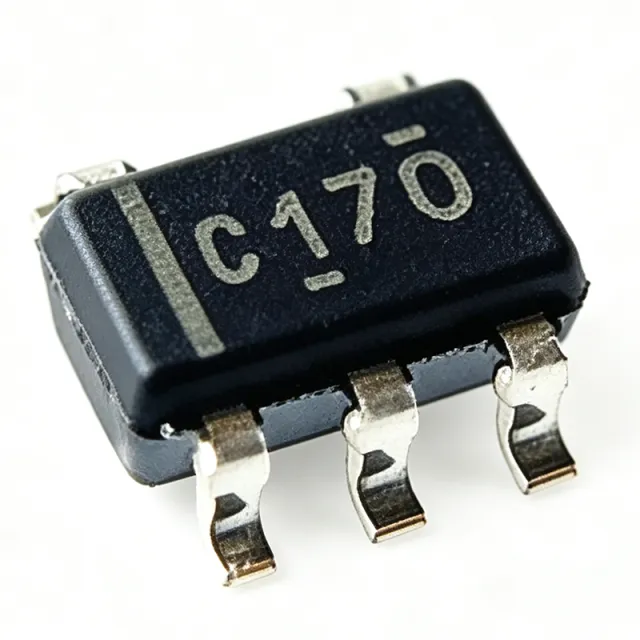
SN74LVC1G17QDBVRQ1 - Auto Schmitt Buffer SOT-23-5 | Texas Instruments
MPN: SN74LVC1G17QDBVRQ1 ✓ Active| Qty | Unit Price | Extended |
|---|---|---|
| 1 | $0.28 | $0.28 |
| 10 | $0.23 | $2.30 |
| 100 | $0.15 | $15.00 |
| 500 | $0.11 | $55.00 |
| 1,000 | $0.09 | $90.00 |
SN74LVC1G17QDBVRQ1 Overview
A Schmitt-trigger buffer is a logic device in the buffer/driver family of the standard CMOS logic IC hierarchy. Unlike a plain buffer, its input incorporates hysteresis, meaning the switching thresholds for rising and falling edges differ. This makes the device tolerant of slow or noisy input edges that would cause multiple transitions (oscillation) in conventional CMOS inputs, conditioning signals from RC timing circuits, sensor outputs, or long cables.
Key features include the wide 1.65V to 5.5V operating supply range enabling use in mixed 1.8V/3.3V/5V systems, Schmitt-action inputs for noisy or slow-rising signals, push-pull output with high drive capability, and operation across the extended -40C to +125C automotive temperature range. The device belongs to TI's controlled-baseline LVC family with one assembly, one test site, and one fabrication site for consistent quality.
The CMOS LVC architecture achieves low static power dissipation with fast propagation delay (typical values around a few nanoseconds depending on VCC; the digchip summary lists 10.7 ns at low supply). The DBV SOT-23-5 package is a compact surface-mount option for space-constrained designs.
Typical applications include automotive ECU level translation and signal buffering, switch debouncing with hysteresis, RC oscillator waveform squaring, sensor signal conditioning, and general-purpose buffering in body electronics, infotainment, and industrial modules.
Design tip: use the Schmitt hysteresis deliberately - pairing this buffer with a slow RC-filtered input (for example, from a comparator-less analog threshold) yields a clean digital edge; keep VCC decoupling (100 nF ceramic) close to the pin for signal integrity.
Drop-in alternatives for SN74LVC1G17QDBVRQ1 — same package, pin-to-pin compatible. Different-package parts requiring PCB rework are excluded.
Variants in this series
Same-series models that are drop-in compatible with SN74LVC1G17QDBVRQ1 (same form factor and footprint) — differing in RoHS Status, Output Type, Function, Logic Family, MSL Level.
Quick Comparison Tool — Select alternative parts for side-by-side comparison:
SN74LVC1G17DBVR
✓ In Stock
$0.07 / Unit
View Datasheet →SN74LVC1G17DBVR
✓ In Stock
$0.07 / Unit
View Datasheet →74LVC1G17GW,125
📋 Reference alternative (not in catalog)
NC7SZ17L6X
📋 Reference alternative (not in catalog)
SN74AUP1G17DBVR
📋 Reference alternative (not in catalog)
SN74LVC1G17QDBVRQ1 Maximum Ratings & Electrical Characteristics
| Function | Single Schmitt-Trigger Buffer (Y = A) |
| Supply Voltage Range | 1.65 V to 5.5 V |
| Logic Family | LVC (CMOS) |
| Output Type | Push-Pull |
| Channels | 1 |
| Input Type | Schmitt Trigger |
| Operating Temperature | -40C to +125C |
| Qualification | AEC-Q100 (Q1 automotive) |
| Package | SOT-23-5 (DBV) |
| Pin Count | 5 |
| Mounting Type | Surface Mount |
| RoHS Status | Pb-Free (RoHS compatible) |
| Green Status | Pb-Free and free of Br/Sb flame retardants (per TI datasheet) |
| Packaging | Tape and Reel (DBVR) |
SN74LVC1G17QDBVRQ1 Pin Configuration
| Pin 1 | A — Schmitt-trigger input |
| Pin 2 | GND — Ground |
| Pin 3 | Y — Push-pull buffer output (Y = A) |
| Pin 4 | NC — No connect |
| Pin 5 | VCC — Supply, 1.65V to 5.5V |
Typical Applications
SN74LVC1G17QDBVRQ1 is suitable for 6 applications: Automotive ECU Signal Buffering, Switch Debouncing and Wetting Current Sensing, RC Oscillator Waveform Squaring, Sensor Signal Conditioning in Industrial Modules, Infotainment and Display Module Logic, Battery Management and Power-Good Monitoring.
Automotive ECU Signal Buffering
In body-control modules, gateway ECUs, and powertrain controllers, sensor and switch signals travel long harness runs and arrive with slow edges and noise. The SN74LVC1G17QDBVRQ1 conditions these signals with Schmitt hysteresis, converting marginal transitions into clean push-pull logic swings. Its 1.65V to 5.5V VCC range lets it interface directly to 5V sensor rails and 3.3V MCU domains, and AEC-Q100 qualification with -40C to +125C operation satisfies automotive quality gates. Place the buffer near the connector to restore edge rate before the signal reaches the microcontroller, using the 100 nF decoupling cap on VCC.
Recommended
Switch Debouncing and Wetting Current Sensing
Mechanical switches and relays bounce for milliseconds and, with an RC filter, also produce slow ramps. A standard CMOS input would oscillate on such edges, but the Schmitt trigger in this buffer thresholds rising and falling transitions at distinct levels, producing exactly one clean output edge per actuation. With a 10 kOhm / 100 nF RC (about 1 ms), the push-pull output delivers a debounced digital signal to an MCU GPIO. Its low static power suits always-on automotive ignition-sense circuits, and the wide 1.65V to 5.5V range covers 3.3V and 5V logic domains without level shifting.
Recommended
RC Oscillator Waveform Squaring
An RC relaxation oscillator or 555-timer-style network produces a capacitor waveform that is triangular or slow-edged; clocking digital logic directly from it causes double-clocking and metastability. Feeding that node into the SN74LVC1G17QDBVRQ1 squares the waveform: hysteresis sets two trip points that create clean, fast edges with defined duty behavior, and the push-pull output drives fanout directly. Operating at 5.5V maximizes hysteresis margin for noisy environments; at 1.8V it squares signals for low-voltage logic. This is a classic single-gate use where the Schmitt input is essential, not optional.
Recommended
Sensor Signal Conditioning in Industrial Modules
Industrial proximity sensors, optocoupler outputs, and comparator-free threshold detectors often drive loads with rise times of microseconds or more, violating standard CMOS input edge-rate requirements. The Schmitt buffer legally accepts these slow edges and regenerates a fast, clean digital signal for the PLC input or MCU. The -40C to +125C range and controlled-baseline manufacturing support industrial quality expectations even though this specific part is the Q1 automotive grade. Use the 1.65V to 5.5V supply flexibility to match either 3.3V controller banks or legacy 5V I/O racks.
Recommended
Infotainment and Display Module Logic
Head units and cluster displays mix 1.8V, 3.3V, and 5V signaling from touch controllers, backlight sensors, and power-good outputs. The SN74LVC1G17QDBVRQ1 buffers power-good and enable signals between domains, and its Schmitt input tolerates the slow, filtered ramps typical of supervisor and RC delay circuits in these modules. High output drive ensures reliable fanout to multiple loads, while low static power keeps standby drain negligible for keep-alive rails. The small SOT-23-5 footprint fits dense board areas around connectors and display flex-cable interfaces.
Recommended
Battery Management and Power-Good Monitoring
Battery-management front ends generate power-good, fault, and pack-status flags through comparators or filtered analog thresholds with slow edges. Buffering these flags with the SN74LVC1G17QDBVRQ1 guarantees clean logic into the BMS MCU, and the Schmitt action prevents chatter near the threshold that could cause false fault interrupts. The 5.5V maximum VCC tolerates transient-high logic rails, and -40C to +125C operation matches under-hood and pack-side temperature requirements. The single-gate SOT-23-5 adds minimal board area to dense AFE cluster layouts.
Recommended
Recommended Products Summary
Engineering reference data for SN74LVC1G17QDBVRQ1 — comparison, design guidance, and compliance information.
Selection Guide
Comparison with Alternatives
| Parameter | This Product | SN74LVC1G17DBVR | 74LVC1G17GW,125 | NC7SZ17L6X | SN74AUP1G17DBVR |
|---|---|---|---|---|---|
| Package | SOT-23-5 (DBV) | SOT-23-5 (DBV) - same | SOT-23-5 - same | SOT-23-5 - same | SOT-23-5 (DBV) - same |
| Brand | Texas Instruments | Texas Instruments | Nexperia | onsemi | Texas Instruments |
| Function | Schmitt buffer Y = A | Schmitt buffer Y = A | Schmitt buffer Y = A | Schmitt buffer Y = A | Schmitt buffer Y = A |
| Output Drive | High (LVC standard drive) | High (same die) | High (LVC equivalent) | High (TinyLogic) | Much lower drive (per TI E2E) |
Key Differentiators
- AEC-Q100 automotive qualification (vs SN74LVC1G17DBVR)
- Wide 1.65V to 5.5V supply with high drive (vs SN74AUP1G17DBVR)
- Schmitt hysteresis vs plain buffer (vs SN74LVC1G34DBVR)
Design Notes
Exploit the Schmitt hysteresis deliberately: any input edge slower than a few ns/V (which would violate standard CMOS input rules) is safely squared by this device. However, do not use the buffer to clean up signals whose amplitude falls between the hysteresis thresholds at the given VCC - consult the VIT+/VIT- tables in the TI datasheet for threshold values at 1.8V, 3.3V, and 5V to guarantee margin in your design.
Place a 100 nF ceramic decoupling capacitor within 2-3 mm of the VCC pin (pin 5) to GND (pin 2). Although a single gate draws little dynamic current, fast push-pull output transitions inject shoot-through current into the supply; local decoupling prevents ground bounce that could shift the Schmitt thresholds. The NC pin (pin 4) may be left floating or tied to GND per TI datasheet guidance.
Do not substitute the SN74LVC1G34 (standard buffer, no hysteresis) in circuits relying on Schmitt action - slow or noisy inputs will oscillate. Similarly, the AUP1G17 alternative is limited to 3.6V VCC and much lower drive; applying 5V to it violates absolute maximums. For automotive production, only the Q1 suffix carries AEC-Q100/PPAP support - the standard SN74LVC1G17DBVR is not qualified for those programs.
Static power dissipation is very low (CMOS), but dynamic power scales as P = Cpd x VCC^2 x f. At 5.5V and high toggle rates, choose the LVC family's lower VCC when system speed allows to cut power and reduce hysteresis-related dissipation. Unused inputs on neighboring gates on the same board should never float, as floating CMOS inputs increase supply noise and can couple into this buffer's input.
Compliance Information
Per TI datasheet: Pb-Free (RoHS compatible) and Green (Pb-Free plus free of Br/Sb flame retardants). AEC-Q100 Q1 automotive catalog per TI product page.


