The SN74LVC8T245PWR from Texas Instruments is an 8-bit non-inverting dual-supply bus transceiver with configurable voltage translation and 3-state outputs, supplied in a 24-pin TSSOP (PW) package on Tape and Reel. Both supply ports, VCCA and VCCB, operate across the full 1.65V to 5.5V range, so one part bridges any pairing of 1.8V, 2.5V, 3.3V, and 5V logic domains in either direction. The device sustains a typical data rate of 100 Mbps with loads up to 15 pF, supports Ioff partial power-down and hot insertion with power-up 3-state outputs, and carries DIR and OE control pins referenced to VCCA. It is RoHS compliant, rated -40C to +85C, and is an active, in-stock part at XAIPART with 99,999 units available and MOQ of 1. Pricing runs from $0.30 at qty 1 down to $0.175 at 1,000 pieces as of 2026-08-30, making it one of the most economical ways to move eight signals between mixed-voltage buses.
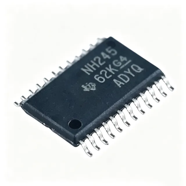
What Is the SN74LVC8T245PWR and Why Do Engineers Use It?
Mixed-voltage systems are the norm: a 1.8V MCU talking to a 3.3V SD card, a 3.3V PLC controller driving 5V industrial I/O, or a 2.5V FPGA bank interfacing a 5V peripheral. The SN74LVC8T245PWR solves this with two independent, supply-referenced port circuits built on low-impedance LVC output drivers. Because each rail (VCCA and VCCB) spans 1.65V to 5.5V independently, the same device performs up-translation (1.8V to 3.3V, 1.8V to 5V) and down-translation (5V to 3.3V, 3.3V to 1.8V) with no external components.
Key verified specifications from the XAIPART database:
| Parameter | Value |
|---|---|
| Function | 8-Bit Dual-Supply Bus Transceiver |
| VCCA range | 1.65 V to 5.5 V |
| VCCB range | 1.65 V to 5.5 V |
| Bits per element | 8 |
| Output type | 3-State |
| Data rate | Typically 100 Mbps |
| Input voltage tolerance | 5.5 V max, regardless of supply |
| Control pin reference | VCCA (DIR, OE) |
| Ioff / power-up 3-state | Yes |
| Hot insertion | Yes |
| Operating temperature | -40C to +85C |
| Package | 24-TSSOP (PW), surface mount |
| Family | 74LVC / Widebus+ |
| Polarity | Non-inverting |
| RoHS | Compliant |
How Do You Design In the SN74LVC8T245PWR? A Practical Technical Guide
Power Connections
Connect VCCA to the lower-voltage domain supply and VCCB to the higher-voltage domain supply (for example, VCCA = 1.8V for an MCU side, VCCB = 3.3V for a card side). Both rails are fully symmetric from 1.65V to 5.5V, so either rail can be the lower one — the A/B naming follows your layout, not a fixed hierarchy. TI's application guidance recommends decoupling both VCCA and VCCB with 0.1uF ceramic capacitors placed close to the pins.
Control Logic: DIR and OE
Both DIR and OE are referenced to VCCA, which simplifies design when the low-voltage controller manages translation. Per the verified pinout, pin 19 is DIR: HIGH drives data A-to-B, LOW drives B-to-A. Pin 1 is OE, an active-low output enable referenced to VCCA. Tie OE to its proper logic level at power-up to avoid leaving the bus in 3-state unintentionally, or deliberately hold it inactive during reset so the FPGA or MCU boots with the external bus released.
Direction and Bus Sharing
The 3-state outputs let multiple boards share one bus: gate each board off the party line with OE during diagnostics or reprogramming, then enable one transceiver at a time. Because the outputs are push-pull LVC drivers (not weak self-directed drivers like the TXB0108), the device needs no pull-up resistors and drives capacitive loads up to 15 pF robustly, preserving clean edges near the typical 100 Mbps data rate.
Partial Power-Down and Hot Insertion
Ioff protection and power-up 3-state outputs block damaging backflow current when either rail is unpowered. This is why the part appears in card slots, backplanes, and pluggable modules: a card can be inserted while the host stays live without latching up or back-powering the card.
Layout Notes
The TSSOP-24 footprint measures a compact 7.8 mm x 4.4 mm, suitable for dense portable layouts. Keep the decoupling caps within a few millimeters of pins 20 (VCCB) and 21 (VCCA), route the eight data lines with matched lengths for parallel buses running near 100 Mbps, and confirm exact pin assignments against the TI datasheet pin diagram before releasing the PCB.
How Do the Pin Functions Map on the TSSOP-24 Package?
The verified pinout from the XAIPART database assigns the A port to pins 2-9, the B port to pins 11-18, with control and power pins arranged around them. Note that OE sits at pin 1 and DIR at pin 19 — always confirm against the datasheet before layout.
What Are the Best Drop-In Alternatives and Equivalents for SN74LVC8T245PWR?
All five alternatives below come from the verified XAIPART alternatives data. The strongest same-footprint substitutes are TI's own family variants; cross-brand equivalents exist from Nexperia and onsemi.
| Part | Relationship | Key Difference (verified) | When to Choose |
|---|---|---|---|
| SN74LVC8T245PWR-EP | TI enhanced-plastic variant | Enhanced-plastic reliability screening, pin-to-pin compatible | Designs specified for extended reliability screening / harsh environments |
| SN74LXC8T245PWR | TI LXC family (newer) | Wider supply range 1.2V-5.5V, same footprint | Systems needing 1.2V logic-domain support |
| SN74AVC8T245PWR | TI AVC family | Faster propagation delay and lower supply option, same 24-TSSOP footprint and dual-rail 1.65V-5.5V architecture | High-speed buses where LVC timing is marginal |
| 74LVC8T245PW (Nexperia) | Cross-brand equivalent | Same dual-rail 1.65V-5.5V architecture and pin-compatible TSSOP-24 footprint; timing and drive differ slightly | Second sourcing; review Nexperia timing tables first |
| MC74LVXC4245DTR2G | Cross-brand dual-supply transceiver | TSSOP-24 footprint compatible [DATA_NEEDED: detailed spec match] | Cross-brand sourcing on the same footprint |
Additional verified substitution notes: the AEC-Q100 qualified SN74LVC8T245QPWRQ1 shares the identical TSSOP-24 footprint and pinout as the commercial PWR, letting one PCB design serve both commercial and automotive grades. TI's E2E forum has confirmed the SN74LVC8T245-EP as an alternate drop-in replacement for the standard part, but the reverse — using the standard part where the -EP was specified — is not recommended. The PWR and PW suffixes are electrically identical: PWR ships in Tape and Reel, PW in Tubes.
Where Does the SN74LVC8T245PWR Fit in Real Applications?
The six verified application scenarios below are drawn directly from the XAIPART product applications database.
| Scenario | Typical Rail Pairing | Verified Specs Used |
|---|---|---|
| SD / SIM card interfaces | VCCA 1.8V, VCCB 3.3V | 1.65-5.5V rails; Ioff + power-up 3-state for hot insertion; 5.5V-tolerant inputs |
| FPGA / MCU I/O bank adaptation | Bank rail to VCCA, peripheral rail to VCCB | 8 bits per element; ~100 Mbps into 15 pF; firmware-switched DIR |
| Industrial 3.3V-to-5V control I/O | VCCA 3.3V, VCCB 5V | -40C to +85C; 5.5V-tolerant inputs; 3-state bus sharing |
| Automotive body and network modules | Same footprint as AEC-Q100 Q1 variant | Ioff for ignition states; DIR/OE referenced to VCCA |
| Test and measurement instruments | Programmable rails set by supervisor/CPLD | ~100 Mbps pattern generation; power-up 3-state prevents DUT contention |
| Portable consumer electronics | 1.8V app processor to 3.3V peripherals | Ioff for power gating; 7.8 mm x 4.4 mm TSSOP-24 footprint |
What Does a Reference Design Look Like? Bridging a 1.8V MCU to a 3.3V SD Card
Problem: An SD/SIM card controller runs at 1.8V while the legacy host PHY uses 3.3V, and the card slot supports hot insertion while the host remains powered.
Approach: Place one SN74LVC8T245PWR in the eight-bit CMD/DAT signal path. Tie VCCA to the 1.8V controller rail and VCCB to the 3.3V card rail — both within the verified 1.65V to 5.5V range. Drive DIR and OE from the 1.8V controller since both controls are referenced to VCCA. Hold OE inactive during card-detect so the bus stays 3-state until the card powers up.
Components: SN74LVC8T245PWR x1; two 0.1uF ceramic decoupling capacitors on VCCA and VCCB placed close to the pins.
Schematic description: MCU 1.8V data bus (8 lines) to A1-A8 (pins 2-9); card-side bus to B1-B8 (pins 18-11); VCCA at pin 21 and VCCB at pin 20, each decoupled to GND (pin 10); DIR (pin 19) and OE (pin 1) from the controller.
Calculations: No external components are required for translation because the dual-rail architecture handles level conversion internally. Margin check: both rails sit well inside the 1.65V-5.5V operating window, and 3.3V logic swings are below the 5.5V input tolerance, giving wide headroom on the card side.
Results: Bidirectional translation with Ioff and power-up 3-state protection during hot insertion, low-impedance LVC drive maintaining signal integrity into 15 pF loads, and a typical data rate of 100 Mbps comfortably covering SD bus timing. [VERIFY_NEEDED: specific SD bus clock speed versus measured propagation delay for the chosen speed grade]
How Much Does the SN74LVC8T245PWR Cost and What Is Its Supply Status?
The part is active in TI's lifecycle and stocked in volume at XAIPART. Verified tier pricing as of 2026-08-30:
| Quantity | Unit Price (USD) |
|---|---|
| 1+ | $0.30 |
| 10+ | $0.2167 |
| 100+ | $0.1917 |
| 500+ | $0.1833 |
| 1,000+ | $0.175 |
Current stock stands at 99,999 units with MOQ of 1 and Tape and Reel delivery, so prototype and production quantities ship without lead-time risk. [DATA_NEEDED: distributor-level allocation and lead-time trends beyond XAIPART stock]. The availability of a pin-compatible automotive variant (SN74LVC8T245QPWRQ1) and an enhanced-plastic variant (-EP) extends the platform across commercial and demanding-grade designs on one footprint.
What Should Buyers Watch Next for This Part?
Three trends anchored to verified data deserve attention. First, lower-voltage logic: the newer TI SN74LXC8T245PWR extends the supply window down to 1.2V on the same footprint, so if your roadmap includes 1.2V I/O banks, qualify the LXC variant now and keep the LVC part as second source. Second, speed pressure: where buses push beyond what the LVC family's typical 100 Mbps and 15 pF drive comfortably cover, the SN74AVC8T245PWR offers faster propagation delay on the identical TSSOP-24 footprint, making it a no-layout-change upgrade path. Third, dual sourcing: the Nexperia 74LVC8T245PW and onsemi MC74LVXC4245DTR2G provide cross-brand fallbacks on the same footprint, but timing and drive figures differ slightly — review the Nexperia and onsemi datasheet timing tables before qualifying the swap. Finally, watch pricing: at $0.175 per unit at 1,000 pieces as of 2026-08-30, this device remains among the lowest-cost eight-channel translators available, and XAIPART's 99,999-unit stock makes it a low-risk line item to consolidate.
Comments
Be the first to comment.
🔐 Please sign in to post a comment.
Don't have an account? Sign up