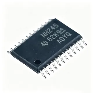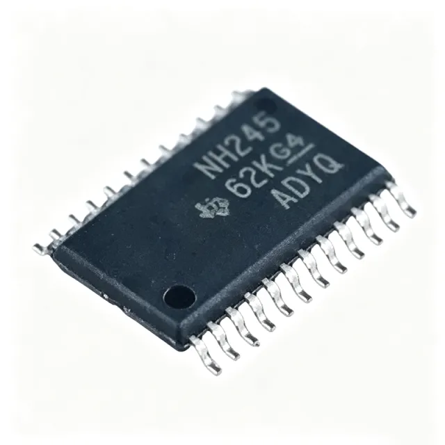
SN74LVC8T245PWR - 8-Bit Dual-Supply Level Translator | TI
MPN: SN74LVC8T245PWR ✓ Active| Qty | Unit Price | Extended |
|---|---|---|
| 1 | $0.3 | $0.30 |
| 10 | $0.2167 | $2.17 |
| 100 | $0.1917 | $19.17 |
| 500 | $0.1833 | $91.65 |
| 1,000 | $0.175 | $175.00 |
SN74LVC8T245PWR Overview
A bus transceiver is a digital logic IC that moves data bidirectionally between two buses, with direction (DIR) and output-enable (OE) controls providing the handshake. The SN74LVC8T245 belongs to the voltage-level translator / logic IC hierarchy and is a member of the TI Widebus+ family, solving the classic mixed-voltage problem in systems where MCUs, FPGAs, and peripherals run on different rails.
Key features include the fully configurable dual-rail architecture, 3-state outputs for bus sharing, mixed-mode signal operation (5V-tolerant I/O with reduced supply), and Ioff plus power-up 3-state support that blocks damaging backflow current during partial power-down and hot-insertion events. DIR and OE are referenced to VCCA, simplifying control-logic design.
Technically, the device uses two independent supply-referenced port circuits with low-impedance LVC output drivers. The typical data rate of 100 Mbps supports SPI, I2C, UART, and parallel bus translation while preserving signal integrity with up to 15 pF load capacitance. Inputs accept voltages up to 5.5V regardless of supply level.
Typical applications include level shifting for SD and SIM card interfaces, sensor and memory modules, 3.3V-to-5V industrial control I/O, and FPGA/CPLD I/O-bank adaptation to external peripherals.
Design tip: decouple both VCCA and VCCB with 0.1uF ceramic capacitors placed close to the pins, tie OE to its proper logic level to avoid a 3-state bus at power-up, and set DIR according to data flow direction. Prices as of 2026-08-30.
Drop-in alternatives for SN74LVC8T245PWR — same package, pin-to-pin compatible. Different-package parts requiring PCB rework are excluded.
Variants in this series
Same-series models that are drop-in compatible with SN74LVC8T245PWR (same form factor and footprint) — differing in Family, Function, Operating Temperature, Package.
Quick Comparison Tool — Select alternative parts for side-by-side comparison:
SN74LVC8T245QPWRQ1
✓ In Stock
$0.72 / Unit
View Datasheet →SN74LVC8T245PWR-EP
📋 Reference alternative (not in catalog)
SN74LXC8T245PWR
📋 Reference alternative (not in catalog)
SN74AVC8T245PWR
📋 Reference alternative (not in catalog)
74LVC8T245PW
📋 Reference alternative (not in catalog)
MC74LVXC4245DTR2G
📋 Reference alternative (not in catalog)
SN74LVC8T245PWR Maximum Ratings & Electrical Characteristics
| Function | 8-Bit Dual-Supply Bus Transceiver |
| Voltage Translation Type | Configurable dual-rail |
| VCCA Supply Range | 1.65 V to 5.5 V |
| VCCB Supply Range | 1.65 V to 5.5 V |
| Bits per Element | 8 |
| Output Type | 3-State |
| Data Rate | Typically 100 Mbps |
| Input Voltage Tolerance | 5.5 V max |
| Control Pins Reference | VCCA (DIR, OE) |
| Ioff / Partial Power-Down | Yes (Ioff and Power-Up 3-State) |
| Hot Insertion Support | Yes |
| Operating Temperature | -40C to +85C |
| Package | 24-TSSOP (PW) |
| Mounting Type | Surface Mount |
| Family | 74LVC / Widebus+ |
| Polarity | Non-Inverting |
| RoHS Status | Compliant |
SN74LVC8T245PWR Pin Configuration
| Pin 1 | OE — Output enable, active low; referenced to VCCA |
| Pin 2 | A1 — Port A data bit 1 |
| Pin 3 | A2 — Port A data bit 2 |
| Pin 4 | A3 — Port A data bit 3 |
| Pin 5 | A4 — Port A data bit 4 |
| Pin 6 | A5 — Port A data bit 5 |
| Pin 7 | A6 — Port A data bit 6 |
| Pin 8 | A7 — Port A data bit 7 |
| Pin 9 | A8 — Port A data bit 8 |
| Pin 10 | GND — Ground |
| Pin 11 | B8 — Port B data bit 8 |
| Pin 12 | B7 — Port B data bit 7 |
| Pin 13 | B6 — Port B data bit 6 |
| Pin 14 | B5 — Port B data bit 5 |
| Pin 15 | B4 — Port B data bit 4 |
| Pin 16 | B3 — Port B data bit 3 |
| Pin 17 | B2 — Port B data bit 2 |
| Pin 18 | B1 — Port B data bit 1 |
| Pin 19 | DIR — Direction control: LOW = B to A, HIGH = A to B; referenced to VCCA |
| Pin 20 | VCCB — Port B supply, 1.65V to 5.5V |
| Pin 21 | VCCA — Port A supply, 1.65V to 5.5V |
Typical Applications
SN74LVC8T245PWR is suitable for 6 applications: SD / SIM Card Interfaces, FPGA / MCU I/O Bank Adaptation, Industrial 3.3V-to-5V Control I/O, Automotive Body and Network Modules, Test and Measurement Instruments, Portable Consumer Electronics.
SD / SIM Card Interfaces
SD and SIM card controllers frequently run at 1.8V while legacy hosts or PHYs use 3.3V. The SN74LVC8T245PWR bridges both domains bidirectionally with VCCA at 1.8V and VCCB at 3.3V, both inside the 1.65V-5.5V range. Its Ioff and power-up 3-state features keep the bus safe during card hot-insertion events, when the card supply may be unpowered while the host is live. Placed directly in the CMD/DAT signal path with 0.1uF decoupling on both rails, the device adds minimal delay while providing 5.5V-tolerant inputs for voltage-swing robustness.
Recommended
FPGA / MCU I/O Bank Adaptation
FPGA banks often supply 1.8V or 2.5V I/O while peripherals, LEDs, and relays expect 3.3V or 5V logic. The SN74LVC8T245PWR ties the bank to VCCA and the peripheral rail to VCCB, translating 8 signals with one package. DIR allows bus direction to be switched under firmware control, and OE tristates the port during reset so the FPGA boots with the external bus released. The low-impedance LVC drivers maintain edges into 15 pF loads at rates near 100 Mbps, comfortably covering parallel address/data buses and memory interfaces.
Recommended
Industrial 3.3V-to-5V Control I/O
Industrial PLC modules, sensor heads, and motor controllers still use 5V signaling for noise robustness while modern microcontrollers operate at 3.3V. With VCCA at 3.3V and VCCB at 5V, the SN74LVC8T245PWR translates control and status lines in both directions. Its -40C to +85C temperature range covers industrial cabinets, and 5.5V-tolerant inputs tolerate supply transients on the 5V rail. The 3-state outputs allow sharing of a status bus among multiple boards, with OE gating each board off the party line during diagnostics.
Recommended
Automotive Body and Network Modules
Automotive ECUs mix 3.3V microcontrollers with 5V sensors and actuator drivers. The AEC-Q100 qualified SN74LVC8T245QPWRQ1 shares the identical TSSOP-24 footprint and pinout as the commercial PWR, allowing one PCB design to serve both grades. Ioff support keeps buses safe during ignition states where some rails are down. DIR and OE referenced to VCCA let the low-voltage MCU manage translation of SENT, GPIO, and diagnostic lines with deterministic control, while 3-state outputs release shared harness-side buses during module reprogramming.
Recommended
Test and Measurement Instruments
Bench instruments interface to devices under test spanning 1.8V, 3.3V, and 5V logic families. The SN74LVC8T245PWR forms the core of a programmable-logic front end: a supervisor or CPLD sets VCCA/VCCB selections or switches rails, and DIR/OE control signal direction per test step. Its approximately 100 Mbps data rate supports fast parallel pattern generation, and power-up 3-state prevents contention with the DUT during connection. Robust LVC drive ensures clean transitions into probe cables and 15 pF loads for reliable level-sensitive measurements.
Recommended
Portable Consumer Electronics
Handheld devices mix 1.8V application processors with 3.3V peripherals such as memory cards, touch controllers, and audio codecs. The SN74LVC8T245PWR bridges eight bidirectional lines between these rails in one low-cost TSSOP-24. Ioff minimizes leakage when subsystems are power-gated for battery savings, and power-up 3-state prevents bus contention during staggered power sequencing. Its low-impedance outputs maintain signal integrity for SDIO and parallel data at tens of megahertz, and the small 7.8 mm x 4.4 mm footprint suits dense portable layouts.
Recommended
Recommended Products Summary
Engineering reference data for SN74LVC8T245PWR — comparison, design guidance, and compliance information.
Selection Guide
Comparison with Alternatives
| Parameter | This Product | SN74LVC8T245QPWRQ1 | SN74LXC8T245PWR | SN74AVC8T245PWR | 74LVC8T245PW (Nexperia) |
|---|---|---|---|---|---|
| Package | TSSOP-24 (PW) | TSSOP-24 (PW) - same | TSSOP-24 (PW) - same | TSSOP-24 (PW) - same | TSSOP-24 - same |
| Brand | Texas Instruments | Texas Instruments | Texas Instruments | Texas Instruments | Nexperia |
| VCCA / VCCB Range | 1.65V to 5.5V | 1.65V to 5.5V | 1.2V to 5.5V | 1.2V to 3.6V (A side) | 1.65V to 5.5V |
| Automotive Grade | No | Yes (AEC-Q100) | No | No | No |
| Bits | 8 | 8 | 8 | 8 | 8 |
| Output Type | 3-State | 3-State | 3-State | 3-State | 3-State |
| Ioff / Power-Up 3-State | Yes | Yes | Yes | Yes | Yes |
| Operating Temperature | -40C to +85C | -40C to +125C | -40C to +85C | -40C to +85C | -40C to +125C |
| Relative Speed | Standard LVC (~100 Mbps) | Standard LVC | Similar, wider supply | Faster (lower tpd) | Standard LVC |
Key Differentiators
- Automotive-qualified same-footprint variant (vs SN74LVC8T245QPWRQ1)
- Wide dual-rail range enables all voltage pairings (vs SN74AVC8T245PWR)
- Wider low-side supply with newer family (vs SN74LXC8T245PWR)
- Second-sourcing option across brands (vs 74LVC8T245PW (Nexperia))
Design Notes
Decouple VCCA and VCCB independently with 0.1uF ceramic capacitors placed within 2 mm of each pin, plus one 4.7uF bulk capacitor per rail. Note that VCCA must be applied for the control inputs DIR and OE to be recognized - if VCCA is delayed relative to VCCB, hold DIR and OE low through the delay to guarantee outputs remain 3-state during power sequencing.
Never leave OE floating - a floating OE can leave the bus in an indeterminate 3-state or drive state at power-up, causing bus contention. Pull OE high (disabled) with a 10k resistor if the controller cannot drive it early. Similarly, do not exceed 5.5V on any input, and remember DIR is referenced to VCCA: driving it from a rail other than VCCA can violate input levels.
Keep A- and B-side traces short and matched for parallel buses; the low-impedance LVC drivers reflect strongly on unterminated lines longer than about 10 cm at 100 Mbps. Add a series 22-33 ohm resistor near the driver if overshoot/ringing is observed. Ioff protection diodes clamp undershoot, but sustained negative ringing below -0.5V should be avoided.
Place the transceiver close to the rail-voltage boundary it serves, and avoid routing translated signals across unrelated domains. Provide a solid ground return shared by both ports; the GND pin is common to both VCCA and VCCB circuits, so ground bounce couples directly between domains.
Compliance Information
RoHS compliant per TI product page and DigiKey listing. Not AEC-Q100 qualified - use SN74LVC8T245QPWRQ1 for automotive. REACH and halogen-free status not stated in provided data.