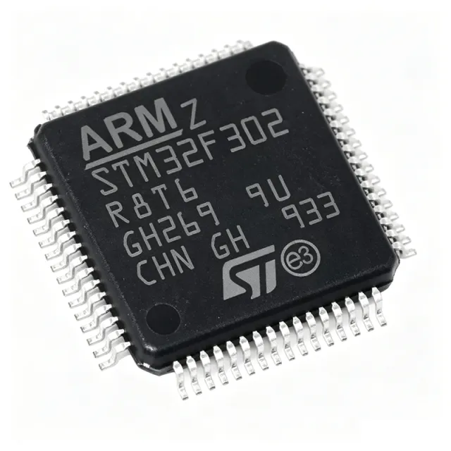
The STM32F302R8T6 is a 64 MHz ARM Cortex-M4F microcontroller with FPU, 64 KB flash, 16 KB SRAM, and a rich analog set (two 12-bit DACs, three 12-bit ADCs up to 5 MSPS, and two op-amps). It is available now from XAIPART: 99,999 units in stock, MOQ 1, and a 1,000-piece price of $5.4091 as of 2026-08-25. This guide gives verified specs, design tips, drop-in alternatives, and market outlook.
Quick Answers
The STM32F302R8T6 is a 64-pin LQFP-64 (10x10 mm) MCU with 51 I/O lines, operating from 2.0V to 3.6V and -40C to +85C. It includes 16 ADC channels, two DAC channels, two op-amps, 7 DMA channels, and I2C, SPI, USART, and CAN interfaces. The device is active and stocked; XAIPART lists 99,999 units and volume pricing that drops from $9.2727 at qty 1 to $5.4091 at qty 1000+.
- Core: ARM Cortex-M4F with FPU
- Memory: 64 KB flash, 16 KB SRAM
- Analog: 16-channel 12-bit ADC up to 5 MSPS, 2-channel 12-bit DAC, 2 op-amps
- Package: LQFP-64, 10x10 mm, 51 I/O
- Availability: Active, 99,999 units in stock
Technical Guide: How to Select and Design In the STM32F302R8T6
Start by validating the memory footprint. 64 KB flash and 16 KB SRAM are enough for moderate-complexity firmware, including motor-control loops and communication stacks. If you need more SRAM or clock speed, consider the pin-compatible STM32F303R8T6 (72 MHz, 40 KB SRAM). If temperature range is the limiting factor, select STM32F302R8T7 (-40C to +105C).
Power Supply and Pin Decoupling
Operate the MCU from 2.0V to 3.6V. Connect all VDD pins to the digital supply, VSS to ground, VDDA to the analog supply, VSSA to analog ground, and VREF+/VREF- to the ADC reference. Place decoupling capacitors close to the power pins, and keep the analog supply VDDA separate from the digital supply through a small ferrite bead if noise is a concern.
Clock Sources
The internal 8 MHz RC oscillator can run basic operations; for precise timing use an external crystal connected to PF0 (OSC_IN) and PF1 (OSC_OUT). The maximum clock frequency is 64 MHz, so design the PLL/clock tree with the required system clock in mind.
Programming and Debug Interfaces
Use the SWD interface on PA13 (SWDIO) and PA14 (SWCLK) for in-circuit programming and debugging. NRST is active low. BOOT0 on pin 45 selects the boot mode, and PB2 is BOOT1.
Analog Signal Chain
The 16-channel 12-bit ADC (up to 5 MSPS) captures current, voltage, or temperature signals. The two 12-bit DACs generate reference voltages or analog control signals. The two op-amps condition sensor or current-shunt outputs, reducing external components. The advanced-control timer generates high-resolution PWM for power and motor control.
Communication and Control Interfaces
The device integrates I2C, SPI, USART, and CAN. Example verified pin assignments include USART1_TX on PA9, USART1_RX on PA10, CAN_RX on PA11, CAN_TX on PA12, I2C1_SCL on PB6, and I2C1_SDA on PB7. This makes it easy to connect sensors, displays, and industrial networks.
Pin Planning for Common Functions
From the verified LQFP-64 pinout, PA0 and PA1 serve as ADC inputs, PA4 and PA5 as DAC outputs, PA8 as TIM1_CH1, PA9/PA10 as USART1, PA11/PA12 as CAN, and PA13/PA14 as SWD. Reserve these pins early in the layout to avoid routing conflicts.
Electrical and Environmental Characteristics
The device is RoHS compliant and operates from 2.0V to 3.6V. The LQFP-64 package is 10x10 mm, surface-mount, and the operating temperature range is -40C to +85C. These parameters define the board-level power and thermal design.
Memory and DMA
With 64 KB flash and 16 KB SRAM, allocate code and data carefully. The 7 DMA channels move ADC conversion results and communication frames without loading the Cortex-M4F core, which is useful for real-time control.
Application-Specific Design Notes
- Motor control: FOC of brushless DC motors using the 12-bit ADC up to 5 MSPS, advanced-control timer, and FPU.
- Power management: Monitor voltage/current with ADC; generate control signals with DAC or PWM.
- Industrial automation: Use CAN, USART, SPI, I2C and 51 I/O pins for PLC/sensor/actuator interfaces.
- Consumer electronics: Small LQFP-64 package and low power modes support portable designs.
- Medical devices: High-resolution 12-bit ADC for physiological monitoring; active lifecycle helps long product life.
- IoT devices: Use sleep modes, local FPU processing, and UART/SPI to wireless modules.
Design Walkthrough: 3-Phase Motor Control
For a field-oriented control (FOC) application, use the advanced-control timer PWM outputs (e.g., TIM1_CH1 on PA8) to drive a three-phase inverter. Sense phase currents with ADC inputs such as PA0 (ADC_IN0) and PA1 (ADC_IN1). Condition the shunt signals with the integrated op-amps before the ADC. Run the Clarke and Park transforms on the Cortex-M4F FPU. Communicate with a host over CAN using PA11/PA12. The on-board DAC can provide current-loop references or analog test outputs.
The 7 DMA channels offload ADC and communication transfers from the core, preserving CPU bandwidth for control loops.
Alternatives & Comparison: Drop-In Replacements for STM32F302R8T6
All alternatives below come from the XAIPART database. The STM32F302R8T7 is the most direct drop-in for extended temperature. The STM32F303R8T6 is pin-compatible but a performance upgrade, so re-verify firmware. The STM32F301R8T6 removes the DAC and lowers analog performance. The STM32F302R8T6TR is the tape-and-reel version of the same die.
| Parameter | STM32F302R8T6 | STM32F302R8T7 | STM32F303R8T6 | STM32F301R8T6 |
|---|---|---|---|---|
| Functional profile | 64 MHz Cortex-M4F with FPU, 64 KB flash, 16 KB SRAM, 2x 12-bit DAC, 2 op-amps, 16-ch 12-bit ADC | Same functional profile, extended temperature -40C to +105C | Higher performance: 72 MHz, 40 KB SRAM | Lower analog performance, no DAC |
| Package | LQFP-64, 10x10 mm, 51 I/O | LQFP-64, pin-compatible | LQFP-64, pin-compatible | Package not specified |
| Analog peripherals | 16-ch 12-bit ADC up to 5 MSPS, 2-ch 12-bit DAC, 2 op-amps | Same analog peripheral set | Enhanced analog set, exact values not specified | No DAC, lower analog performance |
| Drop-in status | Baseline | Drop-in; verify temperature range | Pin-compatible; firmware changes required | Not a drop-in for DAC-dependent designs |
For volume production, the tape-and-reel STM32F302R8T6TR simplifies automated assembly. When swapping to any alternative, always compare the exact pinout and peripheral mapping in the target datasheet.
Industry Insight: Market Position, Lifecycle, and Supply
The STM32F302R8T6 is in active lifecycle status. XAIPART shows 99,999 units in stock, MOQ 1, and the following verified pricing tiers as of 2026-08-25:
| Quantity | Price per unit |
|---|---|
| 1+ | $9.2727 |
| 10+ | $6.697 |
| 100+ | $5.9242 |
| 500+ | $5.6667 |
| 1000+ | $5.4091 |
According to the verified FAQ, lead time typically ranges from 4 to 8 weeks depending on distributor stock and order quantity, and stock availability varies by distributor. Buyers should check real-time inventory before ordering.
Trends & Outlook: What Buyers Should Watch
With an active lifecycle and volume pricing to $5.4091 at 1,000 pieces, the STM32F302R8T6 remains a cost-effective entry point into ST's mixed-signal F3 line. The combination of 64 MHz Cortex-M4F FPU, 12-bit ADC up to 5 MSPS, DAC, op-amps, and CAN aligns with demand for motor control, digital power, and industrial IoT edge nodes.
Watch for continued stock at distributors and the availability of the pin-compatible STM32F303R8T6 as an upgrade path if you need 72 MHz or 40 KB SRAM. Also monitor the active lifecycle status of the F3 series when planning multi-year industrial or medical programs.
Reference
STMicroelectronics STM32F302R8T6 Datasheet (accessed 2026-08-25).
More resources: STM32F302R8T6 product page | STM32F302R8T7 product page | STM32F303R8T6 product page
Comments
Be the first to comment.
🔐 Please sign in to post a comment.
Don't have an account? Sign up