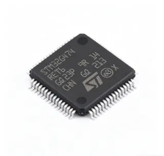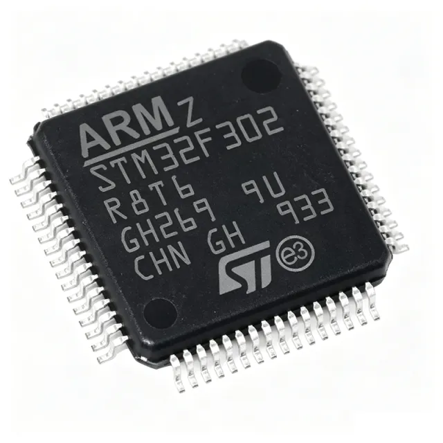
STM32F302R8T6 - 64MHz ARM Cortex-M4F MCU | STMicroelectronics
MPN: STM32F302R8T6 ✓ Active| Qty | Unit Price | Extended |
|---|---|---|
| 1 | $9.2727 | $9.27 |
| 10 | $6.697 | $66.97 |
| 100 | $5.9242 | $592.42 |
| 500 | $5.6667 | $2,833.35 |
| 1,000 | $5.4091 | $5,409.10 |
STM32F302R8T6 Overview
A microcontroller (MCU) is a compact integrated circuit designed to govern a specific operation in an embedded system. It contains a processor core, memory, and programmable input/output peripherals. The STM32F302R8T6 belongs to the STM32F3 family, which is optimized for analog and mixed-signal control applications, bridging the gap between general-purpose MCUs and digital signal processors (DSPs).
Key features include a 64 MHz ARM Cortex-M4F core with FPU, 64 KB flash, 16 KB SRAM, and a rich set of analog peripherals: two 12-bit DACs, three 12-bit ADCs (up to 5 MSPS), and an operational amplifier. It also integrates a 16-bit advanced-control timer, multiple general-purpose timers, and a real-time clock. Communication interfaces include I2C, SPI, USART, and CAN, making it versatile for industrial and consumer applications.
The STM32F302R8T6 leverages the ARM Cortex-M4F architecture with DSP instructions and a single-precision FPU, enabling efficient execution of complex algorithms. The device operates from a 2.0V to 3.6V power supply and supports a temperature range of -40°C to +85°C. Its advanced analog peripherals allow for high-resolution signal acquisition and generation, reducing external component count.
Typical applications include motor control, power management, industrial automation, and consumer electronics. The combination of high-speed ADC, DAC, and op-amp makes it ideal for closed-loop control systems, such as field-oriented control (FOC) of brushless DC motors. The CAN interface supports robust communication in automotive and industrial networks.
When designing with this MCU, ensure proper decoupling of the power supply pins and a stable clock source. The internal 8 MHz RC oscillator can be used for basic operation, but an external crystal is recommended for applications requiring precise timing. The device supports in-circuit programming and debugging via SWD, simplifying firmware development.
Drop-in alternatives for STM32F302R8T6 — same package, pin-to-pin compatible. Different-package parts requiring PCB rework are excluded.
Variants in this series
Same-series models that are drop-in compatible with STM32F302R8T6 (same form factor and footprint) — differing in Communication Interfaces, Flash Memory, Maximum Clock Frequency, Package, SRAM.
Quick Comparison Tool — Select alternative parts for side-by-side comparison:
ATSAMD21G18A-AU
✓ In Stock
$1.74 / Unit
View Datasheet →STM32F302R8T7
📋 Reference alternative (not in catalog)
STM32F302R8T6TR
📋 Reference alternative (not in catalog)
STM32F303R8T6
📋 Reference alternative (not in catalog)
STM32F301R8T6
📋 Reference alternative (not in catalog)
STM32F302R8T6 Maximum Ratings & Electrical Characteristics
| Core | ARM Cortex-M4F with FPU |
| Maximum Clock Frequency | 64 MHz |
| Flash Memory | 64 KB |
| SRAM | 16 KB |
| Supply Voltage | 2.0 V to 3.6 V |
| Operating Temperature | -40C to +85C |
| Package | LQFP-64 (10x10 mm) |
| Mounting Type | Surface Mount |
| Number of I/O Pins | 51 |
| ADC Resolution | 12-bit |
| Number of ADC Channels | 16 |
| DAC Resolution | 12-bit |
| Number of DAC Channels | 2 |
| Operational Amplifiers | 2 |
| Communication Interfaces | I2C, SPI, USART, CAN |
| Timers | Advanced-control, general-purpose, basic |
| DMA Channels | 7 |
| RoHS Status | Compliant |
STM32F302R8T6 Pin Configuration
| Pin 1 | VBAT — Battery backup supply |
| Pin 2 | PC13 — GPIO / RTC output |
| Pin 3 | PC14 — GPIO / OSC32_IN |
| Pin 4 | PC15 — GPIO / OSC32_OUT |
| Pin 5 | PF0 — GPIO / OSC_IN |
| Pin 6 | PF1 — GPIO / OSC_OUT |
| Pin 7 | NRST — Reset (active low) |
| Pin 8 | VDD — Digital power supply |
| Pin 9 | VSS — Ground |
| Pin 10 | VDDA — Analog power supply |
| Pin 11 | PA0 — GPIO / ADC_IN0 |
| Pin 12 | PA1 — GPIO / ADC_IN1 |
| Pin 13 | PA2 — GPIO / USART2_TX |
| Pin 14 | PA3 — GPIO / USART2_RX |
| Pin 15 | PA4 — GPIO / DAC_OUT1 |
| Pin 16 | PA5 — GPIO / DAC_OUT2 |
| Pin 17 | PA6 — GPIO / SPI1_MISO |
| Pin 18 | PA7 — GPIO / SPI1_MOSI |
| Pin 19 | PB0 — GPIO / ADC_IN8 |
| Pin 20 | PB1 — GPIO / ADC_IN9 |
| Pin 21 | PB2 — GPIO / BOOT1 |
| Pin 22 | PB10 — GPIO / I2C2_SCL |
| Pin 23 | PB11 — GPIO / I2C2_SDA |
| Pin 24 | PB12 — GPIO / SPI2_NSS |
| Pin 25 | PB13 — GPIO / SPI2_SCK |
| Pin 26 | PB14 — GPIO / SPI2_MISO |
| Pin 27 | PB15 — GPIO / SPI2_MOSI |
| Pin 28 | PC6 — GPIO / TIM3_CH1 |
| Pin 29 | PC7 — GPIO / TIM3_CH2 |
| Pin 30 | PC8 — GPIO / TIM3_CH3 |
| Pin 31 | PC9 — GPIO / TIM3_CH4 |
| Pin 32 | PA8 — GPIO / TIM1_CH1 |
| Pin 33 | PA9 — GPIO / USART1_TX |
| Pin 34 | PA10 — GPIO / USART1_RX |
| Pin 35 | PA11 — GPIO / CAN_RX |
| Pin 36 | PA12 — GPIO / CAN_TX |
| Pin 37 | PA13 — SWDIO |
| Pin 38 | PA14 — SWCLK |
| Pin 39 | PA15 — GPIO / TIM2_CH1 |
| Pin 40 | PB3 — GPIO / TIM2_CH2 |
| Pin 41 | PB4 — GPIO / TIM2_CH3 |
| Pin 42 | PB5 — GPIO / TIM2_CH4 |
| Pin 43 | PB6 — GPIO / I2C1_SCL |
| Pin 44 | PB7 — GPIO / I2C1_SDA |
| Pin 45 | BOOT0 — Boot mode selection |
| Pin 46 | PB8 — GPIO / CAN_RX |
| Pin 47 | PB9 — GPIO / CAN_TX |
| Pin 48 | VDD — Digital power supply |
| Pin 49 | VSS — Ground |
| Pin 50 | PC10 — GPIO / USART4_TX |
| Pin 51 | PC11 — GPIO / USART4_RX |
| Pin 52 | PC12 — GPIO / USART5_TX |
| Pin 53 | PD2 — GPIO / USART5_RX |
| Pin 54 | VSSA — Analog ground |
| Pin 55 | VREF+ — ADC reference voltage |
| Pin 56 | VREF- — ADC reference ground |
| Pin 57 | PA0 — GPIO / ADC_IN0 |
| Pin 58 | PA1 — GPIO / ADC_IN1 |
| Pin 59 | PA2 — GPIO / USART2_TX |
| Pin 60 | PA3 — GPIO / USART2_RX |
| Pin 61 | PA4 — GPIO / DAC_OUT1 |
| Pin 62 | PA5 — GPIO / DAC_OUT2 |
| Pin 63 | PA6 — GPIO / SPI1_MISO |
| Pin 64 | PA7 — GPIO / SPI1_MOSI |
Typical Applications
STM32F302R8T6 is suitable for 6 applications: Motor Control, Power Management, Industrial Automation, Consumer Electronics, Medical Devices, IoT Devices.
Motor Control
The STM32F302R8T6 is ideal for field-oriented control (FOC) of brushless DC motors. Its 12-bit ADC with up to 5 MSPS sampling rate captures phase currents accurately, while the advanced-control timer generates high-resolution PWM signals. The FPU accelerates the Clarke and Park transforms, enabling efficient real-time control loops. With a 64 MHz clock, the MCU can execute complex algorithms with low latency, ensuring smooth motor operation. The integrated op-amp can condition current-sense signals, reducing external components. For a 3-phase motor, three PWM channels and three ADC channels are used, all available on this device. The CAN interface allows integration into industrial networks for remote monitoring and control. Overall, the STM32F302R8T6 provides a cost-effective solution for high-performance motor control in robotics, drones, and industrial automation.
Recommended
Power Management
In power management systems, the STM32F302R8T6 excels due to its high-speed ADC and DAC. It can monitor voltage and current via the ADC, and generate control signals via the DAC or PWM timers. The 12-bit resolution provides fine granularity for precise regulation. The device's low power consumption in sleep modes makes it suitable for battery-powered applications. The op-amp can be used for signal conditioning of current sense resistors. With multiple communication interfaces, it can report status to a host controller. The wide operating voltage range (2.0V to 3.6V) allows direct connection to common power rails. For a digital power supply, the MCU can implement PID control loops at high frequency, improving transient response. The STM32F302R8T6 is a reliable choice for smart chargers, DC-DC converters, and UPS systems.
Recommended
Industrial Automation
The STM32F302R8T6 is well-suited for industrial automation, including PLCs, sensors, and actuators. Its robust communication interfaces (CAN, USART, SPI, I2C) enable seamless integration into industrial networks. The 12-bit ADC can interface with various sensors, while the DAC can generate analog control signals. The device's operating temperature range (-40°C to +85°C) ensures reliability in harsh environments. The advanced timers can generate precise PWM for controlling valves, heaters, or motors. The FPU accelerates signal processing for predictive maintenance algorithms. With 51 I/O pins, it can interface with many peripherals. The STM32F302R8T6 is a cost-effective solution for distributed control systems, offering high performance and low power consumption. Its long-term availability makes it suitable for industrial products with extended lifecycles.
Recommended
Consumer Electronics
In consumer electronics, the STM32F302R8T6 can be used in smart home devices, wearables, and audio equipment. Its low power consumption and small package make it ideal for portable devices. The DAC can generate audio signals, while the ADC can process sensor data. The FPU enables audio effects processing. The device supports various display interfaces via SPI or I2C. With multiple timers, it can generate tones or control LEDs. The STM32F302R8T6's rich peripheral set allows for a single-chip solution, reducing BOM cost. For a smart thermostat, it can read temperature sensors, control a heater via PWM, and communicate with a smartphone via Bluetooth (external module). The device's reliability and long-term availability make it a preferred choice for consumer products.
Recommended
Medical Devices
The STM32F302R8T6 is suitable for medical devices such as patient monitors, infusion pumps, and diagnostic equipment. Its high-resolution ADC (12-bit) ensures accurate measurement of physiological signals. The FPU enables real-time signal processing for ECG or EEG analysis. The device's low power consumption is critical for battery-operated devices. The CAN interface allows integration into hospital networks. The operating temperature range covers clinical environments. The STM32F302R8T6's reliability and long-term availability are essential for medical applications. For a pulse oximeter, it can read the photodiode signal via ADC, process the data to calculate SpO2, and display results on an LCD. The device's rich peripheral set simplifies design, reducing time-to-market.
Recommended
IoT Devices
The STM32F302R8T6 is an excellent choice for IoT edge nodes. Its low power consumption in sleep modes extends battery life. The device can collect sensor data via ADC and transmit it via UART or SPI to a wireless module. The FPU enables local data processing, reducing cloud dependency. The wide operating voltage range allows direct connection to batteries. With multiple communication interfaces, it can connect to various sensors and actuators. The STM32F302R8T6's small package and low cost make it ideal for mass-produced IoT devices. For a smart agriculture sensor, it can read soil moisture, temperature, and humidity, and send data via LoRa. The device's robustness ensures reliable operation in outdoor environments.
Recommended
Recommended Products Summary
Engineering reference data for STM32F302R8T6 — comparison, design guidance, and compliance information.
Selection Guide
Comparison with Alternatives
| Parameter | This Product | STM32F302R8T7 | STM32F303R8T6 | STM32F301R8T6 | ATSAMD21G18A-AU |
|---|---|---|---|---|---|
| Package | LQFP-64 | LQFP-64 | LQFP-64 | LQFP-64 | TQFP-64 |
| Brand | STMicroelectronics | STMicroelectronics | STMicroelectronics | STMicroelectronics | Microchip Technology |
| Core | ARM Cortex-M4F | ARM Cortex-M4F | ARM Cortex-M4F | ARM Cortex-M4F | ARM Cortex-M0+ |
| Max Clock Frequency | 64 MHz | 64 MHz | 72 MHz | 64 MHz | 48 MHz |
| Flash Memory | 64 KB | 64 KB | 64 KB | 64 KB | 256 KB |
| SRAM | 16 KB | 16 KB | 40 KB | 16 KB | 32 KB |
| ADC Resolution | 12-bit | 12-bit | 12-bit | 12-bit | 12-bit |
| DAC Channels | 2 | 2 | 2 | 0 | 1 |
| CAN Interface | Yes | Yes | Yes | No | No |
Key Differentiators
- Integrated operational amplifiers (vs STM32F301R8T6)
- Higher clock speed and more SRAM (vs ATSAMD21G18A-AU)
- CAN interface (vs STM32F301R8T6)
Design Notes
Decouple all VDD and VDDA pins with 100nF ceramic capacitors placed as close to the pins as possible. Additionally, use a 4.7uF capacitor on VDDA for analog noise filtering. The VREF+ pin should be connected to a clean reference voltage, typically 3.3V, with a 1uF capacitor to ground. Proper decoupling is critical for ADC accuracy and stable operation.
For the LQFP-64 package, ensure a solid ground plane under the device. Route the crystal oscillator (if used) with short traces and keep it away from high-speed digital signals. Place the boot configuration resistors (BOOT0 and BOOT1) with pull-downs to ensure reliable startup. Use a 4-layer PCB for optimal EMC performance.
Do not exceed the absolute maximum ratings: VDD max 3.6V, and any I/O pin voltage must be within VSS-0.3V to VDD+0.3V. Ensure the NRST pin is pulled high with a 100nF capacitor to ground for reliable reset. When using the ADC, avoid floating input pins by configuring them as analog inputs. For CAN communication, terminate the bus with 120 ohm resistors at both ends.
Compliance Information
RoHS compliant per STMicroelectronics product page. Not AEC-Q100 qualified; for automotive, consider STM32F302R8T7 with extended temperature range.