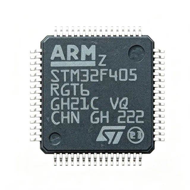
Quick Answers: What Is the STM32F405RGT6 and Is It Available Now?
The STM32F405RGT6 is a 168 MHz ARM Cortex-M4F microcontroller from STMicroelectronics with 1 MB Flash, 192 KB SRAM, 3x 12-bit ADCs, 2x 12-bit DACs, USB 2.0 OTG FS/HS, 2x CAN, and SDIO in an LQFP-64 (10x10 mm) package. It delivers 210 DMIPS and 1.25 DMIPS/MHz, operates from 1.8V to 3.6V, and is rated for -40°C to +85°C. As of 2026-08-20, XAIPART lists 99,999 units in stock with an MOQ of 1, and lifecycle status is active. Pricing is $12.50 at qty 1, $11.20 at qty 10, $9.80 at qty 100, $8.50 at qty 500, and $7.60 at qty 1000. This guide explains selection, design-in details, verified drop-in alternatives, and the supply outlook.
For live inventory and ordering, see the STM32F405RGT6 product page. You can also download the ST datasheet for pin and electrical details.
Technical Guide: How to Select and Design In the STM32F405RGT6
Core, Memory, and Why the Specs Matter
The verified core is an ARM Cortex-M4 with single-precision FPU and a full set of DSP instructions, running up to 168 MHz. The STMicroelectronics description confirms 210 DMIPS and 1.25 DMIPS/MHz, with zero-wait-state execution from Flash using the ART Accelerator. This makes the MCU strong for real-time control and signal processing. The 90 nm process, Memory Protection Unit, 96-bit unique ID, RNG, and CRC unit further support reliable and secure embedded designs.
Memory is 1 MB Flash and 192 KB SRAM. For a 64-pin MCU, this is substantial headroom for control stacks, communication buffers, and data logging. Designers can standardize on one part across multiple products, which simplifies qualification and inventory planning.
Pinout Essentials for Your Schematic
The verified 64-pin LQFP pinout includes 51 GPIOs plus power, reset, boot, debug, and communication pins. In the schematic, prioritize power, reset, boot, debug, and the interfaces your firmware actually uses. The table below lists the functionally key pins; the product page contains the full pin table.
| Pin | Name | Function |
|---|---|---|
| 1 | VBAT | Battery backup supply |
| 7 | NRST | Reset |
| 8 | VSSA | Analog ground |
| 9 | VDDA | Analog power supply |
| 34 | PA11 | GPIO / USB_DM |
| 35 | PA12 | GPIO / USB_DP |
| 36 | PA13 | GPIO / SWDIO |
| 37 | VSS_2 | Ground |
| 38 | VDD_2 | Power supply |
| 39 | PA14 | GPIO / SWCLK |
| 50 | BOOT0 | Boot mode select |
| 51 | PB8 | GPIO / CAN1_RX |
| 52 | PB9 | GPIO / CAN1_TX |
| 53 | VSS_3 | Ground |
| 54 | VDD_3 | Power supply |
PA13 and PA14 are the SWD debug pins, BOOT0 selects the boot mode, and PA11/PA12 carry the USB data lines when USB is enabled. Connect all VDD and VSS pins to their respective rails, and keep VDDA/VSSA separate from the digital supply on the PCB.
Power, Decoupling, and Layout
The verified supply range is 1.8V to 3.6V, so a 3.3V rail is the most common choice, with headroom for lower-voltage operation. The verified description specifically calls out adequate decoupling on the power supply pins and careful layout for high-speed USB and SDIO interfaces. Place bypass capacitors near each VDD pin, keep analog ground returns short, and minimize loop area for USB_DM/USB_DP differential pairs.
The STM32F405RGT6 supports Sleep, Stop, and Standby low-power modes. These modes allow battery-powered designs to reduce consumption between processing bursts.
Peripheral and Interface Planning
Peripheral inventory from the verified database: 51 GPIOs, 3x 12-bit ADCs, 2x 12-bit DACs, 12x 16-bit timers, 2x 32-bit timers, 3x I2C, 4x USART, 2x UART, 3x SPI, 2x CAN, 1x USB 2.0 OTG FS/HS, and 1x SDIO. Multiple GPIOs share alternate functions, so check the datasheet multiplexing table before finalizing the pin map.
For motor control, the FPU, DSP instructions, timers for PWM, and ADCs for current sensing are directly backed by the verified application area. For industrial gateways, the two CAN controllers, USB OTG, and SDIO provide flexible connectivity.
Verified Application Scenarios
The XAIPART database records six primary application areas.
- Motor Control: Run FOC with the 168 MHz FPU core, generate precise PWM with timers, and sample motor currents with the 3x 12-bit ADCs. Suits BLDC, PMSM, and stepper motors.
- Power Conversion: Implement digital PSU and inverter loops with high-speed ADCs and timers, while the FPU accelerates PID and state-space math.
- Industrial Automation: Use 1 MB Flash and 192 KB SRAM for control logic and data logging, and connect through UART, SPI, and CAN to sensors, actuators, and PLCs.
- Medical Devices: Capture and output signals with the 12-bit ADCs and DACs, and use the FPU for ECG/EEG processing; USB handles monitoring links.
- Consumer Electronics: Drive user interfaces and audio processing with 168 MHz and FPU, use USB OTG for host/device connectivity, and use low-power modes for battery operation.
- Drones and UAVs: Run flight control algorithms on the 168 MHz core; interface gyroscopes, accelerometers, GPS, and radios through ADCs, UART, SPI, and timers.
Design Solution: A 20 kHz Motor-Control PWM Example
A common design target is a 20 kHz PWM switching frequency with enough timer resolution for precise duty control. Using the 168 MHz timer clock, set the prescaler to 167 to create a 1 MHz timer clock, then set the auto-reload register to 49:
f_PWM = 168 MHz / ((167 + 1) × (49 + 1)) = 168 MHz / 8400 = 20 kHz.
The 12-bit ADCs return 4096 codes per sample, so current-loop feedback can be mapped across a 0–4095 range. On each PWM cycle, sample phase current, execute FOC calculations on the FPU, and update duty cycles. With 1 MB Flash and 192 KB SRAM, the control stack, telemetry, and bootloader fit on one chip.
Firmware Development and Ecosystem
ST provides STM32CubeIDE and HAL libraries, and the verified FAQ adds support for third-party IDEs such as Keil MDK and IAR EWARM. Start pin configuration with STM32CubeMX-style tools, then layer application code on the HAL. The 96-bit unique ID enables node identity or license binding, while the RNG and CRC unit strengthens communication and data integrity routines.
Alternatives & Comparison: Which Drop-In Replacements Should You Consider?
When requirements change, the XAIPART database lists five verified alternatives. Two are direct drop-in candidates from the verified data: STM32F415RGT6 and GD32F405RGT6. The other three change package or feature set.
| Alternative | Verified Relationship / Key Notes |
|---|---|
| STM32F405RGT6 | Baseline: ARM Cortex-M4 with FPU, 168 MHz, 1 MB Flash, 192 KB SRAM, LQFP-64, 3x 12-bit ADC, 2x 12-bit DAC, USB OTG FS/HS, 2x CAN, SDIO. |
| STM32F415RGT6 | Adds crypto/hash processor, same pinout and memory. Suitable when hardware crypto acceleration is required. |
| STM32F405RGT6TR | Tape and reel packaging variant, same die. Useful for high-volume production ordering. |
| GD32F405RGT6 | Pin-compatible, same ARM Cortex-M4 at 168 MHz, 1 MB Flash, 192 KB SRAM, identical LQFP-64 package. Firmware may need minor adjustments due to HAL differences. |
| STM32F407VET6 | More GPIOs, Ethernet, camera interface, different package (100-pin LQFP). Not a direct form-factor drop-in. |
| STM32F446VCT6 | Higher clock (180 MHz), more SRAM, different package. Choose when performance requires a board change. |
If your board is fixed to LQFP-64, the verified drop-in paths are STM32F415RGT6 and GD32F405RGT6. Validate firmware compatibility and supply position before switching. If the board can change, STM32F407VET6 adds Ethernet and camera interface, while STM32F446VCT6 delivers 180 MHz and more SRAM.
For pricing and inventory on these parts, browse the microcontrollers category at XAIPART.
Industry Insight: What Is the Market Position and Lifecycle Status of the STM32F405RGT6?
Lifecycle status in the XAIPART database is active, which means the part remains suitable for new designs. Supply is healthy: 99,999 units in stock with MOQ 1 as of 2026-08-20.
Verified pricing as of 2026-08-20: $12.50 at qty 1, $11.20 at qty 10, $9.80 at qty 100, $8.50 at qty 500, and $7.60 at qty 1000. The 1000-unit tier is the price anchor for volume planning. XAIPART’s verified supply-chain note in the FAQ lists a typical 52-week lead time, but major distributors such as DigiKey and Mouser currently show stock as of 2026-08-20.
Market-share data is not included in the verified product record, so this article does not estimate it. Use the active lifecycle, stock level, price tiers, and lead time as the sourcing baseline, and confirm stock before a large production order.
Trends & Outlook: What Should Buyers Watch for the STM32F405RGT6?
The verified combination of 168 MHz Cortex-M4F, 1 MB Flash, 192 KB SRAM, 3x 12-bit ADCs, 2x 12-bit DACs, USB OTG FS/HS, 2x CAN, and SDIO keeps this MCU relevant for motor control, power conversion, industrial automation, medical, consumer, and drone designs.
Three trends matter. First, lifecycle continuity: active status and visible stock reduce the pressure to requalify. Second, drop-in sourcing: STM32F415RGT6 adds crypto/hash with the same pinout and memory, and GD32F405RGT6 offers a pin-compatible second source with minor firmware changes. Third, price leverage: the verified tier drops from $12.50 to $7.60 per unit at 1000 pieces as of 2026-08-20, so consolidating orders at volume lowers BOM cost.
If you plan new factory orders, watch the verified 52-week lead time. For immediate builds, use current distributor stock and XAIPART’s 99,999-unit inventory. For production release, order the STM32F405RGT6TR tape-and-reel variant, which uses the same silicon.
For further reading, visit the XAIPART blog and check the STM32F405RGT6 product page for live price and stock updates.
Comments
Be the first to comment.
🔐 Please sign in to post a comment.
Don't have an account? Sign up