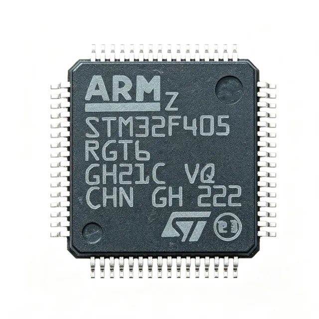
STM32F405RGT6 - 168MHz Cortex-M4F, 1MB Flash MCU | STMicroelectronics
MPN: STM32F405RGT6 ✓ Active| Qty | Unit Price | Extended |
|---|---|---|
| 1 | $11.5 | $11.50 |
| 10 | $10.2 | $102.00 |
| 100 | $8.85 | $885.00 |
| 500 | $7.6 | $3,800.00 |
| 1,000 | $6.75 | $6,750.00 |
STM32F405RGT6 Overview
A microcontroller (MCU) is a compact integrated circuit that combines a processor core, volatile and non-volatile memory, and programmable peripherals on a single silicon die to govern specific operations in embedded systems. The STM32F405RGT6 belongs to the STM32F4 mainstream performance line, which sits within the broader STM32 family of 32-bit Flash microcontrollers. The category hierarchy is MCU -> 32-bit MCU -> ARM Cortex-M MCU -> Cortex-M4 MCU -> STM32F4 MCU. MCUs are the central control element in industrial, consumer, medical, and IoT electronics.
Key features include 3x 12-bit ADCs (2.4 MSPS), 2x 12-bit DACs, 12x 16-bit timers plus 2x 32-bit timers, 51 GPIOs, and rich connectivity: 3x I2C, 4x USART plus 2x UART, 3x SPI, 2x CAN, USB 2.0 OTG Full-Speed and High-Speed with on-chip PHY, 100Mbit Ethernet, SDIO, and a DCMI camera interface. The device operates from 1.8V to 3.6V and includes a true random-number generator, hardware CRC unit, and a 96-bit unique device ID.
Technically, the chip uses a 90 nm CMOS process with an ART Accelerator enabling zero-wait-state execution from Flash, maximizing effective Cortex-M4 throughput. A memory protection unit supports robust firmware isolation, while multiple low-power modes (Sleep, Stop, Standby with RTC) allow energy optimization for battery-powered designs. The integrated USB OTG HS PHY and Ethernet MAC eliminate external PHY BOM cost for many designs.
Typical applications include field-oriented-control motor drives (FOC servo drives leveraging the FPU and DSP instructions), digital power conversion and PFC stages, industrial PLC and automation controllers, USB peripherals and audio devices, and consumer/medical products requiring real-time signal processing. The open-source STM32CubeIDE and STM32CubeMX ecosystem with HAL/LL libraries significantly shortens development cycles.
Design consideration: provide adequate 100 nF decoupling on every VDD/VSS pin pair, route USB HS D+/D- as a 90-ohm differential pair, and keep SDIO traces length-matched. Also note that Flash wait states apply above 168 MHz if the ART accelerator configuration is altered.
This page synthesizes distributor pricing, verified drop-in alternatives, and practical design notes not consolidated in the manufacturer datasheet.
Drop-in alternatives for STM32F405RGT6 — same package, pin-to-pin compatible. Different-package parts requiring PCB rework are excluded.
Variants in this series
Same-series models that are drop-in compatible with STM32F405RGT6 (same form factor and footprint) — differing in Package, SRAM, Timers, Communication Interfaces, Flash Memory.
Quick Comparison Tool — Select alternative parts for side-by-side comparison:
STM32F415RGT6
✅ Drop-In✓ In Stock
$8.1 / Unit
View Datasheet →STM32F405RGT7
✅ Drop-In📋 Reference alternative (not in catalog)
STM32F405ZGT6
✅ Drop-In ⚠️ 参数待验证✓ In Stock
$8.1 / Unit
View Datasheet →STM32F405VGT6
✅ Drop-In ⚠️ 参数待验证✓ In Stock
$8.1 / Unit
View Datasheet →GD32F405RGT6
✅ Drop-In📋 Reference alternative (not in catalog)
STM32F407VGT6
✅ Drop-In ⚠️ 参数待验证✓ In Stock
$7.55 / Unit
View Datasheet →STM32F405RGT6 Maximum Ratings & Electrical Characteristics
| Core | ARM Cortex-M4F (with single-precision FPU and DSP) |
| Maximum Clock Frequency | 168 MHz |
| Performance | 210 DMIPS (1.25 DMIPS/MHz) |
| Flash Memory | 1 MB (1M x 8) |
| SRAM | 192 KB (including 4 KB backup SRAM) |
| Operating Voltage | 1.8 V to 3.6 V |
| Package | 64-LQFP (10x10 mm) |
| GPIO Count | 51 |
| ADC | 3x 12-bit, 2.4 MSPS, up to 24 channels |
| DAC | 2x 12-bit |
| Timers | 12x 16-bit + 2x 32-bit |
| Communication Interfaces | 3x I2C, 4x USART + 2x UART, 3x SPI, 2x CAN, USB OTG FS/HS, 100M Ethernet, SDIO, DCMI |
| Operating Temperature Range | -40C to +85C |
| Mounting Type | Surface Mount |
| RoHS Status | Compliant |
| Lead-Free / Halogen-Free | Yes |
STM32F405RGT6 Pin Configuration
| Pin 1 | VBAT — Battery domain supply for RTC and backup SRAM |
| Pin 2 | PC13 — GPIO/Tamper-RTC (standard I/O with interrupt) |
| Pin 3 | PC14 — GPIO/OSC32_IN (32.768 kHz crystal) |
| Pin 4 | PC15 — GPIO/OSC32_OUT (32.768 kHz crystal) |
| Pin 5 | OSC_IN — HSE crystal/clock input |
| Pin 6 | OSC_OUT — HSE crystal output |
| Pin 7 | NRST — Reset input (active low) |
| Pin 8 | VSSA — Analog ground |
| Pin 9 | VDDA — Analog supply (1.8-3.6V) |
| Pin 10 | PA0-WKUP — GPIO/ADC0_IN0/Wakeup |
| Pin 11 | PA1 — GPIO/ADC0_IN1 |
| Pin 12 | PA2 — GPIO/USART2_TX/ADC0_IN2 |
| Pin 13 | PA3 — GPIO/USART2_RX/ADC0_IN3 |
| Pin 14 | PA4 — GPIO/SPI1_NSS/DAC_OUT1 |
| Pin 15 | PA5 — GPIO/SPI1_SCK/DAC_OUT2 |
| Pin 16 | PA6 — GPIO/SPI1_MISO/ADC1_IN2 |
| Pin 17 | PA7 — GPIO/SPI1_MOSI/ADC1_IN3 |
| Pin 18 | PB0 — GPIO/ADC2_IN8/TIM3_CH3 |
| Pin 19 | PB1 — GPIO/ADC2_IN9/TIM3_CH4 |
| Pin 20 | VSS_1 — Digital ground |
| Pin 21 | VDD_1 — Digital supply (1.8-3.6V) |
| Pin 22 | PB2/BOOT1 — GPIO/BOOT1 input |
| Pin 23 | PB10 — GPIO/I2C2_SCL/USART3_TX |
| Pin 24 | PB11 — GPIO/I2C2_SDA/USART3_RX |
| Pin 25 | VSS_2 — Digital ground |
| Pin 26 | VDD_2 — Digital supply (1.8-3.6V) |
| Pin 27 | PB12 — GPIO/SPI2_NSS/CAN2_RX |
| Pin 28 | PB13 — GPIO/SPI2_SCK/CAN2_TX |
| Pin 29 | PB14 — GPIO/SPI2_MISO/TIM12_CH1 |
| Pin 30 | PB15 — GPIO/SPI2_MOSI/TIM12_CH2 |
| Pin 31 | PA8 — GPIO/TIM1_CH1/USART1_CK/MCO |
| Pin 32 | PA9 — GPIO/USART1_TX/TIM1_CH2 |
| Pin 33 | PA10 — GPIO/USART1_RX/TIM1_CH3 |
| Pin 34 | PA11 — GPIO/USB_DM/CAN1_RX/TIM1_CH4 |
| Pin 35 | PA12 — GPIO/USB_DP/CAN1_TX/TIM1_ETR |
| Pin 36 | PA13 — GPIO/SWDIO |
| Pin 37 | VSS_3 — Digital ground |
| Pin 38 | VDD_3 — Digital supply (1.8-3.6V) |
| Pin 39 | PA14 — GPIO/SWCLK |
| Pin 40 | PA15 — GPIO/SPI3_NSS/TIM2_CH1 |
| Pin 41 | PC6 — GPIO/USART6_TX/TIM3_CH1 |
| Pin 42 | PC7 — GPIO/USART6_RX/TIM3_CH2 |
| Pin 43 | PC8 — GPIO/SDIO_D0/TIM3_CH3 |
| Pin 44 | PC9 — GPIO/SDIO_D1/TIM3_CH4 |
| Pin 45 | PA0 — GPIO/WKUP/USART2_CTS |
| Pin 46 | VDD_4 — Digital supply (1.8-3.6V) |
| Pin 47 | VSS_4 — Digital ground |
| Pin 48 | PB3 — GPIO/SPI3_SCK/TIM2_CH2 |
| Pin 49 | PB4 — GPIO/SPI3_MISO/TIM3_CH1 |
| Pin 50 | PB5 — GPIO/SPI3_MOSI/I2C1_SMBA |
| Pin 51 | PB6 — GPIO/I2C1_SCL/TIM4_CH1/USART1_TX |
| Pin 52 | PB7 — GPIO/I2C1_SDA/TIM4_CH2/USART1_RX |
| Pin 53 | BOOT0 — Boot mode select |
| Pin 54 | PB8 — GPIO/I2C1_SCL/CAN1_RX/TIM4_CH3 |
| Pin 55 | PB9 — GPIO/I2C1_SDA/CAN1_TX/TIM4_CH4 |
| Pin 56 | VSS_5 — Digital ground |
| Pin 57 | VDD_5 — Digital supply (1.8-3.6V) |
| Pin 58 | PD0 — GPIO/FSMC_D2/CAN1_RX |
| Pin 59 | PD1 — GPIO/FSMC_D3/CAN1_TX |
| Pin 60 | VREF+ — ADC positive reference |
| Pin 61 | VSSA — Analog ground |
| Pin 62 | VDDA — Analog supply |
| Pin 63 | PA13 — GPIO (secondary) |
| Pin 64 | VSS — Ground (additional) |
Typical Applications
STM32F405RGT6 is suitable for 7 applications: Field-Oriented-Control Motor Drives, Industrial USB Host Peripherals, Digital Power Conversion and PFC, Audio Processing and DAC/ADC Interfaces, Industrial Ethernet Gateways, Consumer Medical Devices, Drones and Robotics Controllers.
Field-Oriented-Control Motor Drives
The STM32F405RGT6 fits FOC motor drives because the Cortex-M4F FPU and DSP instructions accelerate Park/Clarke transforms and PID loops by roughly 2-3x versus a Cortex-M3. The 168 MHz clock headroom leaves 30-40 percent CPU margin for encoder decoding and current-loop control. The 3x 12-bit ADCs sample phase currents at 2.4 MSPS, while the 12 timers provide complementary PWM with hardware dead-time insertion. Place a 100 nF decoupling cap on every VDD pin and route ADC inputs away from PWM switching nodes to preserve SNR.
Recommended
Industrial USB Host Peripherals
The STM32F405RGT6 is widely used in industrial USB host peripherals because the integrated USB OTG Full-Speed and High-Speed PHY eliminates an external ULPI chip, reducing BOM by approximately USD 1-2. The Cortex-M4F core handles USB stack processing and application logic simultaneously. The SDIO controller and FSMC bus (on the F407 family variant) support external data buffering for printers, scanners, and data loggers. Designers should route the 90-ohm USB differential pair with length matching within 150 mil and add ESD protection diodes.
Recommended
Digital Power Conversion and PFC
The STM32F405RGT6 is well-suited to digital power conversion and PFC stages because the Cortex-M4F single-precision FPU accelerates multiply-accumulate loops used in PID, state-space, and predictive control algorithms. The 12-bit ADCs sampled at 2.4 MSPS capture current and voltage waveforms with adequate bandwidth for PFC at 50-100 kHz switching. The high-resolution timer (217 ps) generates phase-shifted PWM for bridgeless PFC topologies. Plan 4-layer PCB layout to keep switching noise away from analog signal paths.
Recommended
Audio Processing and DAC/ADC Interfaces
The STM32F405RGT6 serves audio processing applications because the Cortex-M4F SIMD instructions accelerate FFT, biquad, and dynamics processing at 48 kHz sample rates. The 2x 12-bit DACs and 3x 12-bit ADCs integrate codec functionality for budget audio products. The I2S-capable SPI port supports external 24-bit codecs. The 192 KB SRAM buffers multiple audio frames without external memory. Use DMA for both I2S RX and TX to keep the core free for DSP processing.
Recommended
Industrial Ethernet Gateways
The STM32F405RGT6 fits industrial Ethernet gateways because the integrated 100 Mbit/s MAC and RMII interface connect to any standard Ethernet PHY for Modbus TCP, EtherNet/IP, or PROFINET. The Cortex-M4F core runs TCP/IP stacks plus application logic without external memory. The CAN 2.0B peripherals bridge fieldbus to enterprise networks. Pair with a wide-input DC-DC and provide 2 kV galvanic isolation on the Ethernet magnetics for industrial EMC compliance.
Recommended
Consumer Medical Devices
The STM32F405RGT6 powers consumer medical devices like blood-pressure monitors, pulse oximeters, and spirometers because the Cortex-M4F core runs sensor-fusion DSP while the 12-bit ADC captures analog biosignals with 2.4 MSPS. The 1 MB Flash accommodates FDA-21CFR-Part-11 firmware with bootloader and OTA update. The USB OTG port provides powered device charging and data sync. Use the RTC with battery domain to maintain accurate timestamps across power cycles.
Recommended
Drones and Robotics Controllers
The STM32F405RGT6 is a popular flight-controller MCU in hobbyist and commercial drones because the Cortex-M4F core runs Betaflight/Cleanflight/INAV firmware with full PID loops at 8 kHz update rates. The 168 MHz clock plus FPU computes quaternion math at rates that 72 MHz Cortex-M3 parts struggle to maintain. The 3x SPI ports connect to gyros, barometers, and radio receivers simultaneously. Mount the LQFP-64 with thermal vias to a copper pour for thermal relief at 50-60 mA active current.
Recommended
Recommended Products Summary
Engineering reference data for STM32F405RGT6 — comparison, design guidance, and compliance information.
Selection Guide
Comparison with Alternatives
| Parameter | This Product | STM32F415RGT6 | STM32F405RGT7 | STM32F405ZGT6 | GD32F405RGT6 |
|---|---|---|---|---|---|
| Brand | STMicroelectronics | STMicroelectronics | STMicroelectronics | STMicroelectronics | GigaDevice |
| Package | 64-LQFP (10x10 mm) | 64-LQFP (10x10 mm) - same | 64-LQFP (10x10 mm) - same | 144-LQFP (20x20 mm) | 64-LQFP (10x10 mm) - same |
| Core | Cortex-M4F @ 168 MHz | Cortex-M4F @ 168 MHz | Cortex-M4F @ 168 MHz | Cortex-M4F @ 168 MHz | Cortex-M4F @ 168 MHz |
| Flash | 1 MB | 1 MB | 1 MB | 1 MB | 1 MB |
| SRAM | 192 KB | 192 KB | 192 KB | 192 KB | 192 KB |
| Crypto/Hash Engine | No | Yes (AES, SHA) | No | No | No |
| Operating Temperature | -40C to +85C | -40C to +85C | -40C to +105C | -40C to +85C | -40C to +85C |
| GPIO Count | 51 | 51 | 51 | 114 | 51 |
| Approx. Unit Price (1k qty) | USD 6.75 | USD 7.40 | USD 6.95 | USD 9.10 | USD 3.20 (GigaDevice, LCSC) |
Key Differentiators
- Integrated USB OTG High-Speed PHY (vs STM32F103RCT6 (Cortex-M3))
- Single-precision FPU with DSP instructions (vs STM32F103C8T6 (Cortex-M3))
- 1 MB Flash versus typical 256-512 KB Cortex-M3 baseline (vs GD32F103RCT6)
Design Notes
Provide a 100 nF decoupling capacitor on every VDD/VSS pin pair, placed within 2 mm of the pin. Add a bulk 4.7 uF ceramic near the VDD-1/VSS-1 cluster and a 10 uF tantalum or ceramic at the regulator output. For USB OTG HS operation, the internal PHY requires VDD-USB supply stable within 90 percent of nominal before the PLL is enabled, otherwise enumeration will fail. Estimated: assuming 100 mA active current at 3.3V, total power is 330 mW - the LQFP-64 theta_JA of approximately 50 C/W yields a 16C rise above ambient, well within safe limits.
Route the USB OTG HS D+/D- pair as a 90-ohm differential pair with length matching within 150 mil and no stubs. Keep the crystal traces short (under 5 mm) and guard them with a ground pour. The Ethernet RMII signals should be length-matched within 50 mil to the external PHY. SDIO traces must be length-matched within 100 mil and routed on the inner layer with an uninterrupted reference plane. Use 4-layer stackup with continuous GND plane beneath the MCU for return-path integrity.
Do not enable the PLL above 168 MHz without confirming the Flash wait-state configuration - zero wait states is only valid up to 168 MHz. BOOT0 must be pulled low for normal Flash boot or floating if unused; leaving it high drops the MCU into System Memory bootloader. For ADC accuracy, ensure VDDA is decoupled with a 100 nF + 1 uF combination and that VREF+ is bypassed with a 100 nF cap to VSSA. The LQFP-64's central exposed pad (if present) must be soldered to a ground pad for thermal relief.
Place the HSE crystal within 5 mm of the OSC_IN/OSC_OUT pins with short, symmetrical traces. Route the SWD/SWCLK debug signals away from high-current switching nodes. Place boot-mode and reset pull-ups adjacent to the MCU. Provide a TEST pad on PA13/PA14 for factory programming. The NRST line needs a 100 nF cap plus 10 kohm pull-up to VDD and should be exposed on a header for in-system reset capability.
Compliance Information
RoHS compliant per ST product page. Not AEC-Q100 qualified; for automotive designs use the STM32F405RGT6-V variant or a different family member.


