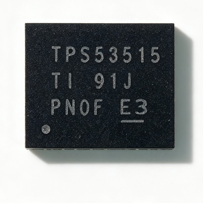
What Is the TPS53515RVER and Why Does It Matter for Your Design?
The Texas Instruments TPS53515RVER is a 12 A synchronous SWIFT step-down buck converter with D-CAP3 adaptive on-time control. It accepts a 1.5 V to 18 V power-stage input (4.5 V to 25 V bias), regulates an adjustable 0.6 V to 5.5 V output from a 600 mV +/-0.5% reference, and integrates 13.8 mOhm high-side and 5.9 mOhm low-side MOSFETs plus a bootstrap switch in a 28-pin VQFN exposed-pad (RVF) package. It is an active-lifecycle part in stock at XAIPART with 99,999 units available, MOQ 1, priced from $5.47 at qty 1 down to $3.18 at 1000 units as of 2026-09-12.
A buck (step-down) converter converts a higher input voltage to a lower regulated output using an inductor, switches, and output capacitors. The TPS53515 sits at the power-management IC level as a fully integrated point-of-load (POL) switching regulator, combining the controller and power stage in one package. That integration is the core value proposition: fewer external parts, smaller board area, and faster time to layout completion than a controller-plus-discrete-FET solution.
Which Verified Specifications Should Engineers Know Before Selecting the TPS53515RVER?
Every figure below comes from the verified XAIPART product database, anchored to the official TI datasheet. These specifications define where the part fits and where it does not.
| Parameter | TPS53515RVER Value |
|---|---|
| Topology | Synchronous buck (step-down) |
| Control Mode | D-CAP3 adaptive on-time |
| Input Voltage Range | 1.5 V to 18 V |
| Bias Voltage Range | 4.5 V to 25 V |
| Output Voltage Range | 0.6 V to 5.5 V |
| Maximum Output Current | 12 A continuous |
| Reference Voltage | 600 mV |
| Reference Tolerance | +/-0.5% |
| High-Side MOSFET RDS(on) | 13.8 mOhm (integrated) |
| Low-Side MOSFET RDS(on) | 5.9 mOhm (integrated) |
| Bootstrap Diode | Integrated boost switch |
| Output Capacitor Support | All ceramic output capacitors |
| Number of Outputs | 1 |
| Package | 28-VFQFN Exposed Pad (RVF) |
| Mounting Type | Surface Mount |
| Operating Temperature | [DATA_NEEDED: operating temperature range] |
| RoHS Status | [DATA_NEEDED: RoHS status] |
Two numbers deserve special attention. First, the 600 mV reference with +/-0.5% tolerance is the accuracy floor for the entire output; on a 0.9 V core rail, that means the converter itself contributes no more than roughly 4.5 mV of setpoint error before divider tolerances [VERIFY_NEEDED: per-derivation accuracy budget including divider resistor tolerance]. Second, the low MOSFET on-resistances are what make 12 A continuous practical in a small VQFN: conduction losses stay manageable without external heat spreading beyond a good exposed-pad copper pour.
The operating temperature range is not listed in the verified database. Confirm it on the official TPS53515 datasheet (PDF) before finalizing a thermally constrained design.
How Do You Design In the TPS53515RVER Step by Step?
Designing in the TPS53515RVER follows a straightforward sequence because the D-CAP3 architecture removes the classic burden of loop compensation.
Step 1: Validate Your Input and Bias Rails
Confirm your power-stage input sits between 1.5 V and 18 V. Most systems driving this part run a 12 V intermediate bus, which sits comfortably inside that window and leaves margin for bus transients. The bias pin must be supplied within its 4.5 V to 25 V range for reliable gate drive; in many 12 V-bus systems, VIN and VBIAS can share the same rail. If your system runs a lower power-stage input, ensure the bias rail independently meets the 4.5 V minimum.
Step 2: Set the Output Voltage
The output is adjustable from 0.6 V to 5.5 V via an external resistor divider from VOUT to the feedback pin, scaled against the 600 mV reference. The design equation is VOUT = 0.6 V x (1 + Rtop/Rbot). For a 0.9 V FPGA core rail, Rtop/Rbot = 0.5; pick standard values consistent with the datasheet FB divider guidance. Because the reference tolerance is +/-0.5%, use low-tolerance divider resistors (0.1% class is common for core rails) [VERIFY_NEEDED: recommended divider resistor tolerances in the datasheet application section].
Step 3: Select the Inductor and Output Capacitors
Select the inductor from the recommended values in the datasheet for stability across the 0.6 V to 5.5 V output range; the verified database does not list specific inductance values, so use the official TI datasheet selection table. For output filtering, the device supports all-ceramic output capacitors. TI's inductor-on-top reference design uses only 10x22 uF ceramic output capacitors and demonstrates 12 mV of output ripple at 12 A load. Eliminating electrolytics improves reliability and board height, particularly valuable in high-vibration industrial environments and low-profile mezzanine cards.
Step 4: Leverage the Integrated Boost Switch
The TPS53515RVER does not require an external bootstrap diode. Place the recommended small ceramic bootstrap capacitor between the BOOT and SW pins per the datasheet application section. This saves a BOM line and layout area on every rail you deploy.
Step 5: Thermal and Layout Discipline
TI's inductor-on-top reference design achieves greater than 87% efficiency with about 2.6 W power loss at 12 A load, and stacking the inductor over the IC reduces X-Y board area. For industrial ambients reaching 70 C to 85 C, validate thermal performance with substantial copper pours on the exposed pad. Follow the datasheet layout section for SW-node loop minimization, which is critical to controlling switching-node ringing and EMI [VERIFY_NEEDED: specific layout guidelines and SW-loop area recommendations from the datasheet layout section].
What Design Performance Can You Expect at Full Load?
Consider a representative design problem: generate a tightly regulated 12 A point-of-load rail from a 12 V intermediate bus in minimal board area, with ceramic-only output filtering.
Approach: Use one TPS53515RVER with VIN and VBIAS tied to the 12 V bus, a feedback divider setting the target output, a single power inductor, and 10x22 uF ceramic output capacitors, mirroring TI's reference design conditions.
Calculations: At a 0.9 V output and full 12 A load, output power is 10.8 W. With the reference design's ~2.6 W total power loss, input power is approximately 13.4 W, giving an estimated efficiency near 80.6% at this low output voltage. The >87% efficiency figure TI publishes applies to the inductor-on-top reference design's stated conditions; efficiency varies directly with output voltage because switching and gate-drive losses represent a larger fraction of a lower output power [VERIFY_NEEDED: exact VOUT condition under which the >87% efficiency figure was measured]. At higher outputs such as 3.3 V or 5 V rails, expect efficiency to rise because output power per amp is greater.
Results: A complete 12 A POL solution in a 28-VFQFN footprint: 0.6 V to 5.5 V adjustable output with +/-0.5% reference accuracy, D-CAP3's fast load-step response, no external bootstrap diode, no compensation network, 12 mV demonstrated ripple with ceramics only, and a parts count low enough to fit beside the load on dense boards.
What Are the Best Alternatives to the TPS53515RVER?
Based on the verified alternatives data, the substitution landscape is narrow and entirely within the TI SWIFT family. No cross-brand pin-to-pin equivalent has been verified in current cross-reference databases, so TI same-family parts are the recommended substitution path.
| Parameter | TPS53515RVER | TPS53513RVER | TPS53125RGER |
|---|---|---|---|
| Maximum Output Current | 12 A continuous | 8 A | [DATA_NEEDED: TPS53125RGER current rating] |
| Control Mode | D-CAP3 adaptive on-time | D-CAP3 (same family) | [DATA_NEEDED: TPS53125RGER control mode] |
| Package | 28-VFQFN Exposed Pad (RVF) | 28-pin VQFN exposed pad (same footprint) | 28-pin QFN class (verify RGE vs RVF land pattern) |
| Substitution Verdict | Reference part | Drop-in only if load < 8 A | Verify footprint and current rating before substitution |
TPS53513RVER: The best footprint-compatible alternative. It shares the 28-pin VQFN exposed-pad footprint and control architecture but is rated for 8 A instead of 12 A, making it a drop-in only where load current stays below 8 A. For lower-current designs, it typically brings cost and efficiency benefits at light-to-medium loads; verify its exact current rating and thermal performance against your maximum load and ambient conditions in its datasheet before finalizing the swap.
TPS53125RGER: For a full 12 A core rail, the TPS53515RVER is the safer choice because its 12 A rating matches the load directly. The TPS53125 shares the 28-pin QFN package class and mounting style per ETEI's comparison, but you must evaluate it against its own datasheet current rating, RDS(on), and theta-JA for thermal performance at 12 A continuous, and confirm the RGE land pattern versus the RVF footprint. When in doubt, derate or choose the TPS53515RVER.
Where Is the TPS53515RVER Used in Real Systems?
The verified application data identifies six strong fit scenarios, each anchored to specific specifications.
- FPGA/ASIC/DSP point-of-load: The 12 A continuous rating covers most core loads, and the 600 mV +/-0.5% reference meets the sub-1% accuracy modern cores require. D-CAP3 handles the sharp transient bursts of clock-domain switching with ceramics only. Reserve the part for loads at or below 12 A; go multi-phase above that.
- Networking and telecom infrastructure: Line cards and switch fabrics distribute a 12 V intermediate bus. The integrated 13.8 mOhm / 5.9 mOhm MOSFETs keep conversion efficient, limiting airflow demand. The trade-off is single-output architecture: one device per rail.
- Industrial DC-DC power stages: The wide 4.5 V to 25 V bias range and all-ceramic capacitor support improve reliability where electrolytics fail in high-vibration environments. Validate thermals with exposed-pad copper pours at 70 C to 85 C ambients.
- Compact, space-constrained power: TI's inductor-on-top reference design proves the part suits height- and area-limited systems: >87% efficiency, ~2.6 W loss at 12 A, 12 mV ripple, and reduced X-Y board area for mezzanine cards and small modules.
- Test and measurement: One qualified design covers 1.0 V digital rails to 5 V interface supplies via the 0.6 V to 5.5 V range. Note that D-CAP3's variable-frequency behavior under light load may require post-regulation for ultra-low-noise analog rails.
- Data center server accessories: BMC cards, storage controllers, and NIC auxiliary circuitry benefit from the 18 V maximum input tolerating bus transients, and from the compact VQFN-28 footprint in dense add-in-card layouts.
What Is the Market Position, Lifecycle Status, and Supply Situation of the TPS53515RVER?
The verified database lists the TPS53515RVER lifecycle status as active, which means TI currently manufactures and supports the part and it is not recommended for new designs to avoid it. This is a favorable procurement signal: active status plus deep stock indicates a healthy supply chain, not an end-of-life risk.
On the supply side, XAIPART lists 99,999 units in stock with MOQ 1 as of 2026-09-12. Authorized distributors including DigiKey, Mouser, and LCSC also report stock: DigiKey ships same-day, Mouser stocks it under order code 595-TPS53515RVET, and LCSC has advertised high-volume pricing near $0.79. When distributor stock depletes, the factory lead time is [DATA_NEEDED: current TI factory lead time]; register for distributor stock alerts if this part anchors a production BOM.
For lifecycle data beyond the active designation, such as projected end-of-life dates or longevity program membership, [DATA_NEEDED: TI longevity/committed-life program status for TPS53515].
How Much Does the TPS53515RVER Cost and How Should You Buy It?
XAIPART's verified tier pricing as of 2026-09-12:
| Quantity | Unit Price (USD) |
|---|---|
| 1+ | $5.47 |
| 10+ | $4.92 |
| 100+ | $4.25 |
| 500+ | $3.72 |
| 1000+ | $3.18 |
The volume curve rewards consolidated BOM purchasing: at 1000 units, you pay roughly 58% of the single-unit price. Stocked distributor orders typically ship within one to two business days. Prices fluctuate with stock and distributor promotions, so request quotes for exact current pricing at your quantity. Buy the TPS53515RVER on XAIPART or browse the full DC-DC converter catalog from Texas Instruments.
What Should Buyers and Engineers Watch Next for the TPS53515RVER?
Anchor your forward planning to the verified specifications and market facts:
- Sub-1V rail trend favors the 600 mV reference. As core voltages in FPGA and ASIC platforms push lower, a 0.6 V +/-0.5% reference with output capability down to 0.6 V keeps this part relevant for next-generation core rails. Design your feedback divider network with headroom for future voltage revisions.
- Electrolytic-free designs are now table stakes. The verified all-ceramic output capacitor support and the 12 mV ripple result with 10x22 uF ceramics mean new designs should never carry electrolytics on this rail, improving reliability profiles and product height budgets.
- Current-density roadmap check. If your load roadmap exceeds 12 A per rail, plan a multi-phase or higher-current architecture now; the verified alternatives do not include a pin-compatible higher-current part, so a redesign cycle is required [VERIFY_NEEDED: TI SWIFT family roadmap beyond 12 A in this package].
- Supply-chain resilience. The only verified footprint-compatible alternate is the 8 A TPS53513RVER, and only for sub-8 A loads. Qualify it early if your design can run below 8 A, giving you a second-source within the same footprint for dual-sourcing strategies.
- Confirm the open data points. Before production release, pull the operating temperature range and RoHS status directly from the current TI datasheet revision, since those two fields are absent from the verified database above.
Key Takeaways for Design and Procurement Teams
- The TPS53515RVER is TI's 12 A D-CAP3 synchronous SWIFT buck: 1.5 V to 18 V input (4.5 V to 25 V bias), 0.6 V to 5.5 V output, 600 mV +/-0.5% reference, integrated 13.8 mOhm / 5.9 mOhm MOSFETs and bootstrap switch, in a 28-VFQFN exposed-pad package.
- Reference-design performance is proven: >87% efficiency, ~2.6 W loss at 12 A, and 12 mV ripple using only 10x22 uF ceramic output capacitors with the inductor-on-top layout.
- The only footprint-compatible alternative is the 8 A TPS53513RVER for sub-8 A loads; the TPS53125RGER needs footprint and current verification. No cross-brand drop-in exists.
- Lifecycle is active with 99,999 units at XAIPART, MOQ 1, $5.47 at qty 1 to $3.18 at qty 1000 as of 2026-09-12.
- Operating temperature range and RoHS status require confirmation from the current TI datasheet revision before production commit.
Comments
Be the first to comment.
🔐 Please sign in to post a comment.
Don't have an account? Sign up