The UCC21540QDWKRQ1 from Texas Instruments is an automotive-grade (AEC-Q100), reinforced-isolated dual-channel gate driver in a 14-pin SOIC (DWK) package. It provides 5700 VRMS galvanic isolation via TI capacitive coupling technology, delivers 4 A peak-source and 6 A peak-sink output current, and drives power MOSFET, IGBT, and GaN transistors. The device is configurable as two low-side drivers, two high-side drivers, or a half-bridge driver with programmable dead time set by a single external resistor, and it includes an 8-V UVLO on the secondary side. As of 2026-09-04, the part is active, in stock at XAIPART with 99,999 units available, MOQ 1, and pricing from $3.27 (qty 1) down to $2.21 (qty 1000+).
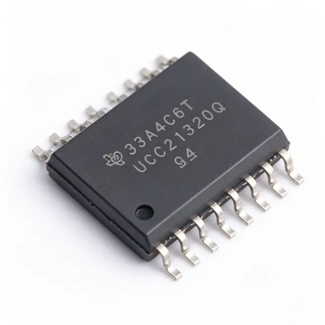
What Is the UCC21540QDWKRQ1 and Why Does It Matter?
An isolated gate driver transfers control signals across a galvanic isolation barrier, allowing a low-voltage controller to safely switch power transistors that float at high potential. The UCC21540QDWKRQ1 performs this function in automotive and industrial power conversion systems, sitting within the gate driver and power management IC hierarchy. Its 5700 VRMS reinforced isolation, achieved through capacitive coupling with 3.3-mm minimum channel-to-channel spacing in the DWK package, supports reinforced-iso creepage requirements in 400 V and 800 V automotive buses.
Unlike optocoupler-based drivers, TI's capacitive isolation technology provides faster and more consistent propagation delay and robust common-mode transient immunity (CMTI). Consistent performance under extreme temperatures makes the -Q1 variant suitable for EV traction inverters, onboard chargers, solar string inverters, and industrial motor drives. The 4 A source and 6 A sink drive strength is well matched to medium-power switches requiring fast turn-off to minimize switching losses.
How Do You Select and Design In the UCC21540QDWKRQ1?
Follow these steps when designing the UCC21540QDWKRQ1 into a half-bridge or dual-driver power stage:
- Choose the configuration. The dual inputs (INH on pin 3, INL on pin 4) let you operate the device as two low-side drivers, two high-side drivers, or a half-bridge driver with independent or interlocked control.
- Size the dead-time resistor. Dead time is programmed with a single external resistor on the DT pin (pin 6). The resistor sets the interlock/dead time between the two outputs in half-bridge mode, preventing shoot-through. Consult the dead-time-versus-resistance table in the TI datasheet and use 1% tolerance resistors for predictable timing.
- Plan the secondary-side supplies. VDDA (pin 10) and VDDB (pin 14) power the two outputs; the 8-V secondary-side UVLO keeps power switches off until the gate-drive rail is stable. Place a low-ESR decoupling capacitor directly across VDDA/VSSA (pins 10/8) and VDDB/VSSB (pins 14/12).
- Verify CMTI margin. Confirm the device's CMTI rating covers the expected dV/dt of your switch node to prevent spurious output transitions. For very fast GaN switch nodes, evaluate the higher-CMTI UCC21550-Q1.
- Use the disable pin. Pulling DIS (pin 5) high forces both outputs low — useful for fault shutdown and startup sequencing.
- Thermal and layout. The device is surface-mount in a 14-SOIC (DWK) package rated for a wide automotive operating temperature range; [DATA_NEEDED: exact operating temperature range values, CMTI figure, propagation delay specifications].
What Is the UCC21540QDWKRQ1 Pinout?
The 14-pin DWK package maps as follows (key functional pins shown; full table on the product page):
| Pin | Name | Function |
|---|---|---|
| 1 | VCCI | Primary-side input supply voltage |
| 2 | GND | Primary-side ground reference |
| 3 | INH | Input A (high-side channel input) |
| 4 | INL | Input B (low-side channel input) |
| 5 | DIS | Disable pin (high = outputs low) |
| 6 | DT | Dead time programming resistor pin |
| 8 | VSSA | Secondary side A ground reference |
| 9 | OUTA | Output A gate drive |
| 10 | VDDA | Secondary side A supply |
| 12 | VSSB | Secondary side B ground reference |
| 13 | OUTB | Output B gate drive |
| 14 | VDDB | Secondary side B supply |
Pins 7 and 11 are no-connect pins within the isolation barrier region. The complete pin table with electrical characteristics lives on the UCC21540QDWKRQ1 product page.
Where Is the UCC21540QDWKRQ1 Used? Real Application Scenarios
Because it combines AEC-Q100 qualification, 5700 VRMS isolation, and 4 A/6 A drive strength, this driver appears across automotive and industrial power conversion:
- EV traction inverter half-bridge: Drives high-side and low-side IGBT or SiC switches; the 4 A source and 6 A sink currents enable fast transitions that reduce switching losses, while programmable dead time prevents shoot-through.
- Onboard charger (OBC) power stage: Provides isolated gate drive for PFC and LLC half-bridge stages; capacitive isolation gives consistent propagation delay across the automotive temperature range, and the 8-V UVLO ensures the switch stays off until the gate-drive rail stabilizes.
- Solar string inverter: The 5700 VRMS isolation and robust CMTI handle the high dV/dt switch nodes typical of SiC and IGBT PV boost and H-bridge stages.
- Industrial motor drives: The 6 A peak-sink current provides fast turn-off to limit short-circuit energy; matched channel propagation delay keeps PWM distortion low for smoother torque.
- GaN-based DC-DC converters: The strong 6 A pull-down discharges the GaN gate quickly to prevent Miller-induced turn-on in totem-pole PFC and CLLC stages — verify CMTI margin against the GaN switch-node slew rate.
- Automotive DC-DC and auxiliary converters: Serves 12 V-to-48 V converters and ADAS bias supplies, with reinforced isolation supporting high-voltage-to-low-voltage bias conversion.
What Are the Alternatives to the UCC21540QDWKRQ1?
The strongest drop-in options stay within the TI family, all sharing the 14-SOIC DWK footprint and dual-channel isolated driver function:
| Parameter | UCC21540QDWKRQ1 | UCC21540DWK | UCC21550-Q1 | UCC21540A-Q1 |
|---|---|---|---|---|
| Qualification | AEC-Q100 (automotive) | Industrial grade (no AEC-Q100) | AEC-Q100 (automotive) | AEC-Q100 (automotive) |
| Positioning | General-purpose reinforced isolated dual driver | Same die and package, industrial | GaN/SiC optimized, higher CMTI | TI-listed alternate variant |
| Optimization | IGBT, Si MOSFET, GaN | IGBT, Si MOSFET, GaN | Fast GaN/SiC switch nodes | Per TI alternate product listing |
[VERIFY_NEEDED: exact electrical spec values (CMTI, propagation delay, UVLO thresholds, drive currents) for UCC21540DWK, UCC21550-Q1, and UCC21540A-Q1 — not provided in current database.] Before substituting, verify dead-time pin mapping and UVLO thresholds in the relevant datasheets. Cross-brand reinforced-isolated dual drivers exist (for example, Analog Devices ADuM4135/ADuM4136 and onsemi NCD57000-family parts per verified FAQ data), but none are guaranteed pin-to-pin compatible with the 14-SOIC DWK footprint, so cross-brand swaps typically require layout changes and re-qualification.
What Does the UCC21540QDWKRQ1 Cost and How Available Is It?
XAIPART pricing as of 2026-09-04: $3.27 at qty 1, $2.95 at qty 10, $2.65 at qty 100, $2.42 at qty 500, and $2.21 at qty 1000+. Stock stands at 99,999 units with MOQ 1, and the lifecycle status is active. The part is also listed in stock at DigiKey, Mouser, and LCSC, with DigiKey offering same-day shipping; lead times for small quantities typically allow 1–5 day delivery. For volume orders above reel quantity, request a factory quote.
How Should Buyers Plan Around This Part? Trends and Outlook
Three buyer-relevant trends anchor directly to verified specs. First, the wide-bandgap transition: the verified data lists MOSFET, IGBT, and GaN as target transistors, and the 6 A sink current supports fast GaN turn-off — but as GaN dV/dt rises, designers should watch whether the higher-CMTI UCC21550-Q1 better fits their topology. Second, automotive electrification: AEC-Q100 qualification and reinforced 5700 VRMS isolation position this part for traction, OBC, and auxiliary converter programs, so locking automotive-qualified supply (choose -Q1 over industrial UCC21540DWK where qualification is required) protects requalification effort. Third, supply planning: with lifecycle status active and 99,999 units in stock at XAIPART as of 2026-09-04, availability is currently healthy, but buyers on automotive programs should secure volume pricing at the 1000-piece break ($2.21, a 32% saving versus single-unit price).
Key Takeaways for Engineers
- The UCC21540QDWKRQ1 delivers 5700 VRMS reinforced isolation with 4 A source / 6 A sink drive in an AEC-Q100, 14-SOIC DWK package with 3.3-mm channel-to-channel spacing.
- Programmable dead time via a single DT-pin resistor simplifies half-bridge shoot-through prevention; use 1% tolerance for predictable timing.
- The 8-V secondary-side UVLO and DIS pin provide safe startup and fault shutdown behavior.
- Configurable as dual low-side, dual high-side, or half-bridge — one part covers multiple topologies from OBC LLC stages to motor-drive half-bridges.
- Family drop-ins (UCC21540DWK, UCC21540A-Q1, UCC21550-Q1) preserve the DWK footprint; verify pin mapping and UVLO before substitution.
- Pricing runs $2.21–$3.27 as of 2026-09-04 depending on quantity, with 99,999 units in stock at XAIPART.
Comments
Be the first to comment.
🔐 Please sign in to post a comment.
Don't have an account? Sign up