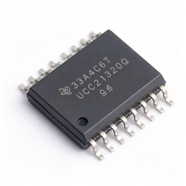
UCC21540QDWKRQ1 - 5.7kVRMS Isolated Dual Gate Driver | Texas Instruments
MPN: UCC21540QDWKRQ1 ✓ Active| Qty | Unit Price | Extended |
|---|---|---|
| 1 | $3.27 | $3.27 |
| 10 | $2.95 | $29.50 |
| 100 | $2.65 | $265.00 |
| 500 | $2.42 | $1,210.00 |
| 1,000 | $2.21 | $2,210.00 |
UCC21540QDWKRQ1 Overview
An isolated gate driver is a power-management IC that transfers control signals across a galvanic isolation barrier, allowing a controller on the low-voltage side to safely switch power transistors floating at high potential. Isolated gate drivers sit within the broader hierarchy of gate drivers, power management ICs, and semiconductors, and are essential building blocks in any switched-mode power conversion system where the switch node is referenced to a high-voltage rail.
Key features include 5700 VRMS reinforced isolation, 8-V UVLO on the secondary side, configurable dual inputs allowing the device to operate as two low-side drivers, two high-side drivers, or a half-bridge driver with independent or interlocked control, and programmable dead time implemented via a single external resistor. The DWK package offers 3.3-mm minimum channel-to-channel spacing for reinforced isolation and a wide operating temperature range suited to automotive under-hood environments.
Architecturally, the device uses TI capacitive isolation technology, which provides faster and more consistent propagation delay than optocoupler-based drivers, along with robust common-mode transient immunity. Consistent performance under extreme temperature conditions makes the -Q1 variant suitable for traction inverters, onboard chargers, and other automotive power systems.
Typical applications include EV traction inverter half-bridges driving IGBT or SiC/GaN modules, onboard charger and DC-DC converter power stages, solar string inverters, and industrial motor drives. The 4 A/6 A drive strength is well matched to medium-power switches requiring fast turn-off to minimize switching losses.
Design tip: size the dead-time resistor precisely and place a low-ESR decoupling capacitor directly across VDDA/VSSA and VDDB/VSSB; verify that the CMTI rating covers the expected dV/dt of your switch node to prevent spurious output transitions.
Drop-in alternatives for UCC21540QDWKRQ1 — same package, pin-to-pin compatible. Different-package parts requiring PCB rework are excluded.
Variants in this series
Same-series models that are drop-in compatible with UCC21540QDWKRQ1 (same form factor and footprint) — differing in Package, Isolation Rating, Isolation Type, Operating Temperature, Isolation Technology.
Quick Comparison Tool — Select alternative parts for side-by-side comparison:
UCC21530Q-Q1
✓ In Stock
$2.1 / Unit
View Datasheet →UCC21520Q-Q1
✓ In Stock
$2.85 / Unit
View Datasheet →ADUM4136BRWZ
✓ In Stock
$2.11 / Unit
View Datasheet →UCC21540DWK
📋 Reference alternative (not in catalog)
UCC21550-Q1
📋 Reference alternative (not in catalog)
UCC21540A-Q1
📋 Reference alternative (not in catalog)
UCC21540QDWKRQ1 Maximum Ratings & Electrical Characteristics
| Number of Channels | 2 |
| Isolation Type | Reinforced, capacitive coupling |
| Isolation Voltage | 5700 VRMS |
| Peak Source Current | 4 A |
| Peak Sink Current | 6 A |
| Channel-to-Channel Spacing | 3.3 mm minimum (DWK package) |
| Dead Time | Programmable (external resistor) |
| Target Transistors | Power MOSFET, IGBT, GaN |
| Configuration Options | Dual low-side, dual high-side, or half-bridge |
| UVLO | 8 V (secondary side) |
| Automotive Qualification | AEC-Q100 |
| Package | 14-SOIC (DWK) |
| Mounting Type | Surface Mount |
| Operating Temperature | Wide temperature range (automotive) |
| RoHS Status | Compliant |
UCC21540QDWKRQ1 Pin Configuration
| Pin 1 | VCCI — Primary-side input supply voltage |
| Pin 2 | GND — Primary-side ground reference |
| Pin 3 | INH — Input A (high-side channel input) |
| Pin 4 | INL — Input B (low-side channel input) |
| Pin 5 | DIS — Disable pin (high = outputs low) |
| Pin 6 | DT — Dead time programming resistor pin |
| Pin 7 | NC — No connect / isolation barrier region |
| Pin 8 | VSSA — Secondary side A ground reference |
| Pin 9 | OUTA — Output A gate drive |
| Pin 10 | VDDA — Secondary side A supply |
| Pin 11 | NC — No connect / isolation barrier region |
| Pin 12 | VSSB — Secondary side B ground reference |
| Pin 13 | OUTB — Output B gate drive |
| Pin 14 | VDDB — Secondary side B supply |
Typical Applications
UCC21540QDWKRQ1 is suitable for 6 applications: EV Traction Inverter Half-Bridge, Onboard Charger (OBC) Power Stage, Solar String Inverter, Industrial Motor Drives, GaN-Based DC-DC Converters, Automotive DC-DC and Auxiliary Converters.
EV Traction Inverter Half-Bridge
The UCC21540QDWKRQ1 drives the high-side and low-side IGBT or SiC switches in automotive traction inverter half-bridge legs. Its 4 A source and 6 A sink currents enable fast switching transitions that reduce switching losses, while programmable dead time prevents shoot-through. The 5700 VRMS reinforced isolation and AEC-Q100 qualification make it suitable for the 400 V/800 V automotive traction bus, and the DWK package's 3.3-mm channel-to-channel spacing supports reinforced isolation creepage requirements.
Recommended
Onboard Charger (OBC) Power Stage
In EV onboard chargers, the UCC21540QDWKRQ1 provides isolated gate drive for PFC and LLC converter half-bridge power stages. The capacitive isolation delivers consistent propagation delay across the full automotive temperature range, important for phase-shifted LLC topologies, and the 8-V UVLO ensures the power switch stays off until the gate-drive rail is stable. The programmable dead time allows one resistor to tune dead time for ZVS timing optimization across battery voltage ranges.
Recommended
Solar String Inverter
Solar string inverters require reinforced isolated gate drivers for their boost and H-bridge stages to bridge controller ground to power-switch potential. The UCC21540QDWKRQ1's 5700 VRMS isolation and robust CMTI handle high dV/dt switch nodes typical of SiC and IGBT PV stages. Its dual-channel half-bridge configuration with interlock simplifies dead-time control in the inverter bridge, and consistent temperature behavior keeps switching timing stable from cold mornings to peak-noon enclosure temperatures.
Recommended
Industrial Motor Drives
Three-phase industrial motor drives use the UCC21540QDWKRQ1 to drive IGBT half-bridge modules in each phase. The 6 A peak-sink current provides the fast turn-off needed to limit short-circuit energy, and the programmable interlock/dead time prevents leg shoot-through with a single resistor setting. The wide automotive temperature range comfortably covers industrial ambient extremes, and consistent propagation delay across channels keeps PWM distortion low for smoother motor torque.
Recommended
GaN-Based DC-DC Converters
High-density GaN DC-DC converters benefit from the UCC21540QDWKRQ1's 4 A/6 A drive capability, which switches GaN FETs quickly with the strong 6 A pull-down required to discharge the gate fast and prevent Miller-induced turn-on. The isolated dual-channel configuration supports half-bridge topologies such as totem-pole PFC and CLLC stages in server and telecom power. Designers should verify CMTI margin against the GaN switch-node slew rate, or consider the higher-CMTI UCC21550-Q1.
Recommended
Automotive DC-DC and Auxiliary Converters
The UCC21540QDWKRQ1 serves isolated auxiliary power converters in vehicles, including 12 V to 48 V converters and safety-critical bias supplies for ADAS domains. AEC-Q100 qualification plus robust performance under extreme temperature conditions ensure consistent switching behavior across the automotive thermal envelope. The reinforced isolation supports the functional isolation requirements of high-voltage-to-low-voltage bias conversion in EV power distribution architectures.
Recommended
Recommended Products Summary
Engineering reference data for UCC21540QDWKRQ1 — comparison, design guidance, and compliance information.
Selection Guide
Comparison with Alternatives
| Parameter | This Product | UCC21540DWK | UCC21550-Q1 | UCC21540A-Q1 |
|---|---|---|---|---|
| Package | 14-SOIC (DWK) | 14-SOIC (DWK) - same | 14-SOIC (DWK) - same | 14-SOIC (DWK) - same |
| Brand | Texas Instruments | Texas Instruments | Texas Instruments | Texas Instruments |
| AEC-Q100 Qualified | Yes | No (industrial grade) | Yes | Yes |
Key Differentiators
- Automotive AEC-Q100 qualification (vs UCC21540DWK)
- Asymmetric 4 A source / 6 A sink drive strength (vs UCC21550-Q1)
- Reinforced isolation with 3.3-mm channel-to-channel spacing (vs UCC21540A-Q1)
Design Notes
Place a low-ESR 0.1 uF ceramic bypass capacitor in parallel with a 10 uF capacitor directly across each secondary supply pin pair (VDDA/VSSA and VDDB/VSSB), as close to the pins as possible. Keep the gate-drive loop (driver output, gate resistor, power transistor, return path) as small as possible to minimize loop inductance and ringing. Follow the PCB layout guidelines in the TI UCC21540-Q1 datasheet for the DWK package creepage and clearance zones.
The 8-V UVLO on the secondary side holds outputs low until the gate-drive rail is valid. For IGBT applications needing higher gate charge, confirm the VDD supply can deliver peak gate current pulses of 4 A source / 6 A sink; size the bulk capacitor at each VDD pin to supply these pulses without drooping below UVLO. For negative gate-drive configurations, bias VSS accordingly and verify the absolute maximum ratings in the datasheet.
In half-bridge mode, the dead-time resistor on the DT pin must be sized per the datasheet resistance-to-dead-time table with 1% tolerance; an incorrect value risks shoot-through at high load current. Also verify the switch-node dV/dt is within the device common-mode transient immunity rating - excessive dV/dt can cause spurious output pulses. Disable (DIS) pin should not be left floating in noise environments; tie it appropriately.
Compliance Information
AEC-Q100 automotive qualification per TI product page. RoHS and lead-free status per standard TI automotive product offering; REACH and halogen-free status not stated in provided data.







