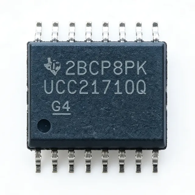
What Is the UCC21710QDWRQ1 and Why Should Power Designers Care?
The UCC21710QDWRQ1 from Texas Instruments is an automotive-grade, galvanically isolated single-channel gate driver designed for up to 1700V SiC MOSFETs and IGBTs. It delivers ±10A peak source and sink current, a 5700 Vrms isolation rating with a 1500 Vrms working voltage, a typical propagation delay of 60 ns, and CMTI of 100 V/ns (typical). The device is AEC-Q100 qualified, operates from -40°C to +150°C, and comes in a 16-pin SOIC (DW) surface-mount package. As of 2026-09-04, the part is active in lifecycle status, with 99999 units in stock at XAIPART, MOQ of 1, and pricing from $4.85 at qty 1 down to $3.10 at qty 1000.
A gate driver is the power amplifier that sits between the control stage (microcontroller or DSP) and the power stage (SiC MOSFETs or IGBTs). The UCC21710-Q1 adds SiO2 capacitive galvanic isolation across that link, protecting low-voltage control circuitry from high-voltage transients and ground loops. Its feature set — DESAT overcurrent protection, active Miller clamp, fault reporting, input/output side UVLO, and an isolated analog-to-PWM sensor — is engineered to reduce switching losses and increase system robustness in traction inverters, on-board chargers, DC-DC converters, motor drives, solar inverters, and industrial power supplies.
This guide consolidates everything a buyer or engineer needs: verified specifications, design-in guidance, packaging alternatives, availability data, and what to watch in this product segment. All data is anchored to the XAIPART verified product database and the TI datasheet at https://www.ti.com/lit/gpn/UCC21710-Q1.
What Are the Verified Key Specifications of the UCC21710QDWRQ1?
The following table lists the verified specifications from the XAIPART product database:
| Parameter | Value |
|---|---|
| Manufacturer | Texas Instruments |
| Category | Power MOSFET Drivers |
| Isolation Type | Capacitive Coupling (SiO2) |
| Isolation Rating | 5700 Vrms |
| Working Voltage | 1500 Vrms |
| Peak Output Current | ±10 A |
| Number of Channels | 1 |
| Input Supply Voltage | 3 V to 5.5 V |
| Output Supply Voltage | 12.8 V to 18 V |
| Propagation Delay | 60 ns (typical) |
| CMTI | 100 V/ns (typical) |
| Overcurrent Protection | Yes (DESAT) |
| Active Miller Clamp | Yes |
| Fault Reporting | Yes |
| Operating Temperature | -40°C to +150°C |
| Package | 16-SOIC (DW) |
| Mounting Type | Surface Mount |
| Automotive Grade | AEC-Q100 Qualified |
| Lifecycle Status | Active |
Three specifications define this part's positioning. First, the 5700 Vrms isolation rating with 1500 Vrms working voltage supports 1700V-class SiC and IGBT power stages. Second, the ±10A peak output current enables fast switching of large power transistors, directly reducing switching losses. Third, the 100 V/ns typical CMTI keeps the isolation barrier reliable in the noisy dv/dt environment of SiC switching.
How Do You Design In the UCC21710QDWRQ1? A Practical Technical Guide
Power Supply and Logic Interface
The input side accepts a 3 V to 5.5 V supply, making it compatible with typical microcontroller and DSP logic rails. The output side requires a 12.8 V to 18 V supply (VDD on pin 8, with VEE on pin 9), covering the gate-drive voltage windows of both IGBTs and SiC MOSFETs. Ensure both input-side and output-side supplies are well decoupled; the device includes input and output side power supply UVLO, which keeps the driver output safely defined during startup and brownout.
PCB Layout for Isolation and Switching Integrity
TI's guidance in the verified data is explicit: use short, low-inductance gate drive loops and provide adequate creepage and clearance for the isolation rating. Keep the OUT (pin 10) to power-transistor-gate loop as compact as possible, and route the return path (VEE/GND2) directly beneath or adjacent to the gate trace. Maintain the creepage and clearance distances across the isolation barrier consistent with the 5700 Vrms isolation and 1500 Vrms working voltage ratings [VERIFY_NEEDED: exact board-level creepage/clearance distances per datasheet tables].
DESAT Overcurrent Protection Setup
The DESAT function (pin 12) requires an external diode and resistor network to sense the collector-emitter (or drain-source) voltage of the power switch during the on-state. When the monitored voltage exceeds the DESAT threshold, the device initiates fast fault response — within 100 ns per the verified feature description — protecting the power stage from short-circuit damage. The shunt current sensing input (OC, pin 13) should be filtered to avoid false triggering from switching noise [VERIFY_NEEDED: recommended DESAT blanking time and filter component values].
Active Miller Clamp Usage
Connect the CLMP pin (pin 11) to the gate of the power transistor. During high dv/dt events at the switch node, the Miller clamp prevents false turn-on by holding the gate low, which is essential when driving high-speed SiC MOSFETs where dv/dt can exceed the 100 V/ns CMTI capability of the surrounding environment.
Isolated Analog-to-PWM Sensing
The AIN (pin 6) and AOUT (pin 7) pair implements the isolated analog-to-PWM sensor, allowing temperature or voltage measurement across the isolation barrier without an additional isolated amplifier. This is valuable for thermal management in on-board chargers and for bus voltage monitoring in solar inverters.
Status and Fault Signaling
The FLT (pin 4) and RDY (pin 5) outputs report fault and ready status to the controller, enabling systematic fault handling in functional-safety-conscious automotive designs [VERIFY_NEEDED: fault response timing details beyond the 100 ns fast fault response figure].
How Do You Decode the Pinout of the UCC21710QDWRQ1?
The functionally key pins from the verified pinout table are summarized below. The full pin table lives on the UCC21710QDWRQ1 product page.
| Pin | Name | Function |
|---|---|---|
| 1 | IN | Input signal |
| 2 | VCC | Input supply voltage (3 V to 5.5 V) |
| 3 | GND | Input ground |
| 4 | FLT | Fault output |
| 5 | RDY | Ready output |
| 6 | AIN | Analog input (isolated sensing) |
| 7 | AOUT | Analog output (isolated sensing) |
| 8 | VDD | Output supply voltage (12.8 V to 18 V) |
| 9 | VEE | Output negative supply |
| 10 | OUT | Gate drive output |
| 11 | CLMP | Miller clamp |
| 12 | DESAT | Desaturation detection |
| 13 | OC | Overcurrent sense |
| 14 | GND2 | Output ground |
Note that pins 15 and 16 are no-connect (NC) pins per the verified pinout.
What Are the Best Alternatives to the UCC21710QDWRQ1?
Within the verified XAIPART database, the drop-in alternative is the UCC21710QDWQ1:
| Parameter | UCC21710QDWRQ1 | UCC21710QDWQ1 |
|---|---|---|
| Die / Function | UCC21710-Q1 isolated gate driver | Same die, identical function |
| Peak Output Current | ±10 A | ±10 A (same die) |
| Isolation Rating | 5700 Vrms | 5700 Vrms (same die) |
| Package | 16-SOIC (DW) | 16-SOIC (DW) |
| Packaging Format | Tape-and-reel ('R' suffix) | Tube packaging |
| Pin Compatibility | — | Pin-compatible, interchangeable |
Per the verified data, the UCC21710QDWRQ1 and UCC21710QDWQ1 are the same device; the 'R' suffix indicates tape-and-reel packaging while the non-R version ships in tube packaging. Both are electrically identical and pin-compatible, so they are interchangeable in designs. Choose tape-and-reel for automated assembly lines and tube packaging for prototyping or low-volume hand assembly. [DATA_NEEDED: pricing and stock for UCC21710QDWQ1].
Where Is the UCC21710QDWRQ1 Used? Verified Application Scenarios
Traction Inverters in Electric Vehicles
The ±10A peak current and 5700 Vrms isolation ensure reliable switching of high-voltage rails, while DESAT overcurrent protection safeguards the inverter during short circuits. AEC-Q100 qualification and the -40°C to +150°C range meet automotive reliability requirements, and the 100 V/ns CMTI prevents false triggering in the noisy motor-drive environment.
On-Board Chargers (OBCs)
In EV OBCs, the device drives SiC MOSFETs in the PFC and DC-DC stages. The 5700 Vrms isolation and 1500 Vrms working voltage handle AC-DC isolation requirements, and the isolated analog-to-PWM sensor enables temperature sensing across the barrier. UVLO protection ensures safe startup and shutdown, and the 16-SOIC package fits space-constrained designs.
Isolated DC-DC Converters
The 60 ns typical propagation delay enables high-frequency operation, and the active Miller clamp prevents false turn-on during high dv/dt transients. Fault reporting and DESAT protection enhance safety on high-voltage buses.
Industrial Motor Drives
The high CMTI (100 V/ns) ensures stable operation against fast transients from motor back-EMF, ±10A drive reduces torque ripple through faster switching, and DESAT with fault reporting prevents damage during overloads.
Solar Inverters
The isolation ratings handle DC bus voltages up to 1500V, and the isolated sensing channel can monitor temperature or voltage across the barrier, improving system monitoring in outdoor environments with wide temperature swings.
Industrial Power Supplies
The 5700 Vrms isolation provides safety isolation for AC-DC and DC-DC converters, the fast 60 ns propagation delay supports high-frequency operation, and UVLO plus overcurrent protection enhance reliability.
What Does a Typical Design Solution With the UCC21710QDWRQ1 Look Like?
Consider an EV on-board charger PFC stage driving a 1200V-class SiC MOSFET with the UCC21710QDWRQ1. The controller operates from a 3.3 V rail — within the verified 3 V to 5.5 V input supply range — connected to VCC (pin 2) with IN (pin 1) driven by the PWM output. The isolated output side uses a 15 V supply, within the 12.8 V to 18 V output supply range, feeding VDD (pin 8) with VEE (pin 9) referenced to the SiC source. OUT (pin 10) drives the gate through a low-inductance loop; CLMP (pin 11) connects to the gate for Miller clamping; DESAT (pin 12) monitors the drain through the external diode-resistor network; OC (pin 13) senses shunt current with an RC filter. FLT (pin 4) and RDY (pin 5) connect back to the controller for fault handling, and AIN (pin 6) accepts a heatsink temperature signal that is recovered as PWM on AOUT (pin 7) at the controller side.
Design validation focuses on verified parameters: confirm the 60 ns typical propagation delay fits the dead-time budget, confirm switch-node dv/dt stays within the 100 V/ns CMTI capability, and confirm worst-case junction temperature remains within the -40°C to +150°C operating range. [VERIFY_NEEDED: gate charge of the target SiC MOSFET for peak-current and switching-loss calculations; specific dead-time and thermal dissipation figures].
What Is the Market Position, Lifecycle Status, and Supply Situation of the UCC21710QDWRQ1?
Per the verified database, the UCC21710QDWRQ1 is in active lifecycle status and is available now at XAIPART with 99999 units in stock as of 2026-09-04, MOQ of 1. It is an AEC-Q100 qualified automotive-grade part from Texas Instruments, positioned in the Power MOSFET Drivers category. Verified pricing tiers as of 2026-09-04 are: $4.85 at qty ≥1, $4.36 at qty ≥10, $3.88 at qty ≥100, $3.49 at qty ≥500, and $3.10 at qty ≥1000. [DATA_NEEDED: market share, lifecycle forecast, and multi-year supply commitment data].
The FAQ data in the database also notes availability through authorized distributors such as DigiKey, Mouser, and LCSC; a database FAQ entry cites LCSC at $2.0848 as of 2026-08-19 [VERIFY_NEEDED: third-party distributor pricing and stock as this figure comes from a dated database FAQ rather than the current XAIPART price file].
What Should Buyers and Engineers Watch Next for This Component Class?
Anchor your roadmap decisions to the verified spec set. The 5700 Vrms isolation and 1500 Vrms working voltage position this driver for 1700V-class SiC and IGBT stages, so watch your bus voltage roadmap: designs staying at or below 1500V working voltage can standardize on this part without moving to higher-isolation SKUs. The ±10A peak drive and 60 ns typical propagation delay support high-frequency SiC switching; if you push switching frequency higher, verify thermal performance of the 16-SOIC (DW) package at your target ambient within the -40°C to +150°C range. The 100 V/ns typical CMTI provides headroom for fast SiC edges — track your switch-node dv/dt as SiC generations evolve. Finally, the supply picture is strong today (active lifecycle, 99999 units in stock as of 2026-09-04); for volume programs, secure pricing at the qty ≥1000 tier of $3.10 and consider qualifying the tube-packaged UCC21710QDWQ1 as a second sourcing option, since the verified data confirms it is the same die and pin-compatible.
How Do You Buy the UCC21710QDWRQ1 on XAIPART?
Order directly on the UCC21710QDWRQ1 product page — 99999 units in stock as of 2026-09-04, MOQ 1, with tiered pricing from $4.85 down to $3.10. For design resources, browse the XAIPART technical blog and other parts in the Power MOSFET Drivers category. Full electrical characteristics are in the official TI datasheet: UCC21710-Q1 datasheet.
Comments
Be the first to comment.
🔐 Please sign in to post a comment.
Don't have an account? Sign up