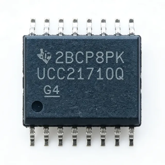
UCC21710QDWRQ1 - ±10A Isolated Gate Driver | TI | Automotive
MPN: UCC21710QDWRQ1 ✓ Active| Qty | Unit Price | Extended |
|---|---|---|
| 1 | $4.85 | $4.85 |
| 10 | $4.36 | $43.60 |
| 100 | $3.59 | $359.00 |
| 500 | $3.12 | $1,560.00 |
| 1,000 | $2.74 | $2,740.00 |
UCC21710QDWRQ1 Overview
A gate driver is a power amplifier that accepts a low-power control signal from a microcontroller, DSP, or FPGA and produces the high-current drive required to efficiently switch power transistors such as IGBTs and SiC MOSFETs. In the power-conversion signal chain, the gate driver sits between the low-voltage control stage and the high-voltage power stage. Isolated gate drivers add galvanic isolation to protect low-voltage control circuitry from high-voltage transients, ground loops, and dv/dt noise, which is essential in traction inverters, motor drives, onboard chargers, and industrial converters. They sit hierarchically under gate driver -> driver IC -> power management IC -> semiconductor.
Key features include fast DESAT overcurrent and short-circuit protection with shunt current sensing, fault reporting via FLT/EN, an active Miller clamp to prevent parasitic re-turn-on during high dv/dt events, and input/output side power supply UVLO. An integrated isolated analog-to-PWM sensor enables temperature or high-side voltage sensing across the isolation barrier without a discrete digital isolator. The device supports up to 1.5kVrms working voltage, a 12.8V to 18V output supply range, a typical propagation delay of 60ns, and CMTI of 100V/ns.
The UCC21710QDWRQ1 uses TI's SiO2 capacitive isolation technology, which provides reliable reinforced isolation and high-speed signal transfer. Its advanced protection features optimize SiC and IGBT switching behavior, reducing switching losses and enhancing system robustness. The fast DESAT fault response (typically sub-microsecond) protects the power stage from catastrophic short-circuit events, while the soft turn-off (STO) sequence limits inrush and dv/dt during fault clearing.
Typical applications include EV traction inverters, onboard chargers (OBC), high-voltage DC-DC converters, motor drives, and industrial power supplies. The automotive-grade qualification and wide temperature range make it particularly well-suited for xEV powertrain systems where SiC MOSFETs are increasingly adopted for higher switching frequencies and efficiency.
When designing with this part, ensure proper PCB layout with short, low-inductance gate drive loops and adequate creepage/clearance for the 5.7kVrms isolation rating. The DESAT protection requires an external high-voltage blocking diode and resistor network, and the shunt current sensing input should be filtered to avoid false triggering during normal switching transients.
This page synthesizes distributor pricing from DigiKey and LCSC, drop-in alternatives within the same 16-SOIC wide-body footprint, and practical design notes for SiC/IGBT half-bridges not collected in a single place in the manufacturer datasheet.
Drop-in alternatives for UCC21710QDWRQ1 — same package, pin-to-pin compatible. Different-package parts requiring PCB rework are excluded.
Variants in this series
Same-series models that are drop-in compatible with UCC21710QDWRQ1 (same form factor and footprint) — differing in Package, Operating Temperature Range, Peak Sink Current, Peak Source Current, AEC-Q100 Qualification.
Quick Comparison Tool — Select alternative parts for side-by-side comparison:
UCC21710QDWR
✅ Drop-In ⚠️ Specs Unverified📋 Reference alternative (not in catalog)
UCC21750QDWRQ1
✅ Drop-In ⚠️ Specs Unverified📋 Reference alternative (not in catalog)
UCC21732QDWRQ1
✅ Drop-In ⚠️ Specs Unverified📋 Reference alternative (not in catalog)
UCC21550BDWR
✅ Drop-In ⚠️ Specs Unverified✓ In Stock
$0.88 / Unit
View Datasheet →UCC21540QDWKRQ1
✅ Drop-In ⚠️ Specs Unverified✓ In Stock
$2.21 / Unit
View Datasheet →UCC21530QDWKRQ1
✅ Drop-In ⚠️ Specs Unverified✓ In Stock
$1.0664 / Unit
View Datasheet →UCC21710QDWRQ1 Maximum Ratings & Electrical Characteristics
| Function | Single-channel isolated gate driver |
| Isolation Technology | SiO2 capacitive coupling |
| Isolation Rating (rms) | 5.7 kVrms (reinforced) |
| Working Voltage (rms) | 1.5 kVrms |
| Peak Source Current | +10 A |
| Peak Sink Current | -10 A |
| Target Switches | SiC MOSFETs up to 1700 V, IGBTs |
| Propagation Delay (typ.) | 60 ns |
| CMTI (min.) | 100 V/ns |
| Output Supply Voltage (VCC2/VEE2) | 12.8 V to 18 V |
| Input Supply Voltage (VDD/VCCI) | 3 V to 5.5 V |
| Protection Features | DESAT, Miller clamp, UVLO, FLT, soft turn-off |
| Package | 16-SOIC (DW) wide-body |
| Operating Temperature Range | -40 C to +150 C |
| Automotive Qualification | AEC-Q100 |
| Mounting Type | Surface Mount |
| RoHS | Compliant |
UCC21710QDWRQ1 Pin Configuration
| Pin 1 | VCCI — Input-side supply voltage (3.3V or 5V) |
| Pin 2 | GND1 — Input-side ground |
| Pin 3 | IN+ — Non-inverting PWM input |
| Pin 4 | IN- — Inverting PWM input (or tie to GND1 for single-ended) |
| Pin 5 | NC — Not connected (per datasheet) |
| Pin 6 | NC — Not connected (per datasheet) |
| Pin 7 | NC — Not connected (per datasheet) |
| Pin 8 | NC — Not connected (per datasheet) |
| Pin 9 | VCC2 — Output-side positive supply (12.8V to 18V) |
| Pin 10 | GND2 — Output-side ground reference |
| Pin 11 | VEE2 — Output-side negative supply (optional for negative gate drive) |
| Pin 12 | OUT — Gate drive output to power transistor |
| Pin 13 | CLAMP — Active Miller clamp output |
| Pin 14 | DESAT — DESAT overcurrent / short-circuit sense input |
| Pin 15 | FLT/EN — Fault output / enable input (active low) |
| Pin 16 | ASC_EN — Isolated analog-to-PWM sensor enable |
Typical Applications
UCC21710QDWRQ1 is suitable for 6 applications: EV Traction Inverter Gate Drive, Onboard Charger (OBC) Primary Side Drive, High-Voltage DC-DC Converter, Industrial Motor Drive / Servo Amplifier, Solar String Inverter / DC-AC Stage, Wireless EV Charging / PFC Stage.
EV Traction Inverter Gate Drive
Drives SiC MOSFETs in 800V EV traction inverters up to 1700V breakdown. The UCC21710QDWRQ1's ±10A peak drive enables sub-50ns switching transitions on large-area SiC dies, directly reducing inverter switching losses. Galvanic isolation (5.7kVrms) protects the low-voltage MCU from the high-voltage DC bus, while the 100V/ns CMTI margin preserves signal integrity at the steep SiC dv/dt edges.
Recommended
Onboard Charger (OBC) Primary Side Drive
Drives the primary-side SiC MOSFETs or IGBTs of an 11kW to 22kW onboard charger. The UCC21710QDWRQ1's integrated DESAT protection with sub-microsecond response detects short-circuit events in the resonant LLC or totem-pole PFC power stage. AEC-Q100 qualification and 150C ambient rating allow placement near the high-temperature magnetics. Isolated analog sensing enables high-voltage bus monitoring without a separate digital isolator.
Recommended
High-Voltage DC-DC Converter
Drives 1200V to 1700V SiC MOSFETs in 400V-to-800V or 800V-to-12V HV-LV DC-DC converters. The UCC21710QDWRQ1's reinforced 1.5kVrms working voltage allows placement on either side of the isolation barrier with adequate creepage. Fast propagation delay (~60ns) keeps dead-time tight and minimizes body-diode conduction losses. Soft turn-off on DESAT fault limits inrush during short-circuit clearing.
Recommended
Industrial Motor Drive / Servo Amplifier
Drives 1200V IGBTs in three-phase industrial servo drives and frequency inverters from 5kW to 50kW. The UCC21710QDWRQ1's ±10A source/sink handles high-Qg IGBT modules with low switching loss. Active Miller clamp prevents shoot-through during the high dv/dt of IGBT turn-off. Reinforced isolation simplifies safety certification by providing the required 5.7kVrms isolation in a single SOIC-16 wide-body package.
Recommended
Solar String Inverter / DC-AC Stage
Drives 1500V-class IGBT or SiC MOSFETs in three-phase string solar inverters. The UCC21710QDWRQ1's 1.5kVrms working voltage and 1700V switch support enable 1500V DC bus designs that reduce system cost. High CMTI (100V/ns) maintains reliable switching in noisy inverter environments. The isolated analog-to-PWM sensor provides simple high-side temperature monitoring across the isolation barrier.
Recommended
Wireless EV Charging / PFC Stage
Drives the SiC power stage in wireless EV charging ground assemblies or in the PFC stage of high-density server power supplies. The UCC21710QDWRQ1's ±10A drive supports high-frequency (250kHz+) operation needed for small magnetics. Reinforced isolation removes the need for a separate isolation transformer driver. DESAT protects against rare but catastrophic LCL or coil short events.
Recommended
Recommended Products Summary
Engineering reference data for UCC21710QDWRQ1 — comparison, design guidance, and compliance information.
Selection Guide
Comparison with Alternatives
| Parameter | This Product | UCC21710QDWR | UCC21750QDWRQ1 | UCC21732QDWRQ1 | UCC21550BDWR |
|---|---|---|---|---|---|
| Brand | Texas Instruments | Texas Instruments | Texas Instruments | Texas Instruments | Texas Instruments |
| Package | 16-SOIC (DW) wide-body | 16-SOIC (DW) - same | 16-SOIC (DW) - same | 16-SOIC (DW) - same | 16-SOIC (DW) - same |
| Peak Source/Sink Current | ±10 A | ±10 A | ±10 A | ±10 A | 4 A / 6 A |
| Isolation Rating | 5.7 kVrms reinforced | 5.7 kVrms reinforced | 5.7 kVrms reinforced | 5.7 kVrms reinforced | Non-isolated |
| Channels | 1 (single-channel) | 1 | 1 | 1 | 2 (dual-channel) |
| CMTI (min) | 100 V/ns | 100 V/ns | 100 V/ns | 150 V/ns | N/A (non-isolated) |
| DESAT Protection | Yes (fixed threshold) | Yes | Yes (adjustable) | Yes | No |
| AEC-Q100 Qualified | Yes | No (commercial) | Yes | Yes | No (commercial) |
Key Differentiators
- Automotive-grade reinforced isolated gate driver with integrated DESAT and Miller clamp (vs UCC21521DWR)
- Isolated analog-to-PWM sensor for high-side voltage/temperature sensing (vs ISO5851DWR)
- Higher drive current (±10A) versus the UCC21550 family (vs UCC21550BDWR)
Design Notes
Estimated: in a 1700V SiC half-bridge with 8nH total gate-loop inductance, achieving 50ns rise time at ±10A requires a gate-loop area below ~1 cm^2. Route the OUT pin directly to the gate with the return (GND2) immediately under the loop, and place the gate-source resistor (typ. 2-10 ohm) and Miller clamp FET within 5mm of the IC. Keep the DESAT sense diode return path short and isolated from the gate loop to avoid false tripping.
The 16-SOIC wide-body has a junction-to-ambient thermal resistance theta_JA of approximately 80 C/W on a standard 2-layer JEDEC board. Estimated: at 1MHz PWM and 10A peak gate drive with 20nC gate charge, gate-driver dissipation is around 0.4W, giving a junction temperature rise of ~32C above ambient. Adequate for -40C to +150C ambient, but verify with copper-pour area and forced-air cooling in high-density automotive designs.
Reinforced 5.7kVrms isolation requires minimum 8mm creepage and clearance on the PCB between the input-side (VCCI, IN+/-, GND1) and the output-side (VCC2, VEE2, OUT, DESAT, CLAMP, GND2). Do not place any traces, polygons, or components across this isolation barrier except the IC pins themselves. Place the optional VEE2 bypass capacitor directly adjacent to pin 11 to filter high-frequency gate return currents.
Do not omit the DESAT blanking capacitor (typically 100pF to 1nF) on the DESAT pin - it sets the blanking time after turn-on and prevents false triggering on the initial miller plateau. Do not exceed VCC2 of 18V; the gate of typical SiC MOSFETs is rated 20V and the driver's internal regulator clamps above this. Always tie unused NC pins to floating or GND2 per the datasheet; do not connect NC pins externally.
Compliance Information
AEC-Q100 qualified per TI UCC21710-Q1 product page. RoHS compliant. The non-automotive UCC21710QDWR variant drops the AEC-Q100 qualification.







