The XC7K325T-2FFG676I is a high-performance AMD Kintex-7 Field Programmable Gate Array fabricated on a 28nm HKMG process, delivering 326,080 logic cells, 840 DSP slices, 16,404,480 bits of block RAM, and 400 user I/Os in a 676-ball FCBGA package. It operates from a 0.97V to 1.03V core supply, reaches a maximum operating frequency of 470.37 MHz at the -2 speed grade, and is rated for industrial temperatures of -40°C to 100°C (TJ). It supports mainstream standards including PCIe Gen3 and 10 Gigabit Ethernet. As of 2026-08-30, the device is in active lifecycle status with deep stock (99,999 units) at XAIPART, priced from $98 at 1,000-unit volume with MOQ of 1. The 'I' suffix denotes the industrial temperature grade; the pin-compatible XC7K325T-2FFG676C covers the commercial 0°C to 85°C range.
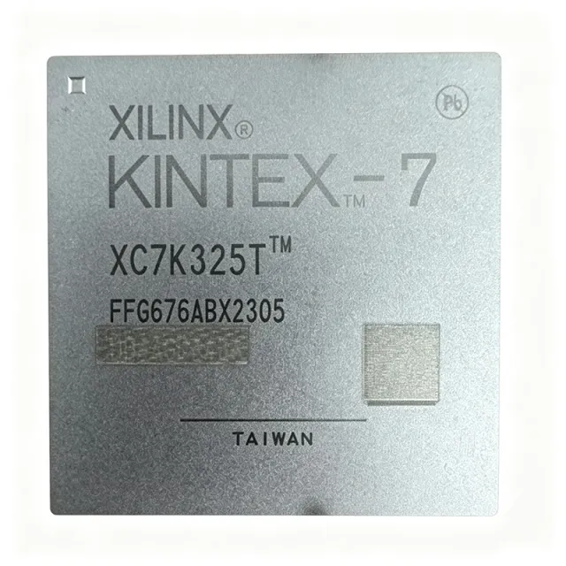
What Is the XC7K325T-2FFG676I and Why Do Engineers Choose It?
The XC7K325T-2FFG676I belongs to AMD's (formerly Xilinx) Kintex-7 family, which sits between the cost-optimized Artix-7 and the high-performance Virtex-7 families. Per the verified database, this device provides 326,080 logic elements/cells organized into 25,475 LABs/CLBs, 16,404,480 total RAM bits, 840 DSP slices, and 400 user I/Os. Clock generation is handled by 10 MMCMs and 4 PLLs in advanced clock management tiles (CMTs). The device is surface-mount, packaged in a 676-BBGA FCBGA, and RoHS compliant.
Engineers choose this part when they need an optimal balance of price, performance, and power: hardened memory controllers, high-speed transceivers, and PCIe blocks reduce external component count, while the -2 speed grade balances throughput against power consumption [VERIFY_NEEDED: exact transceiver count and per-lane data rates are not provided in the verified data].
How Do You Select the Right Speed Grade and Temperature Grade?
Selection hinges on two suffix decisions. First, the speed grade: the -2 grade in this part supports a maximum operating frequency of 470.37 MHz. The XC7K325T-1FFG676I offers a lower -1 speed grade with reduced maximum frequency; choose -1 only for cost-sensitive designs that do not need 470.37 MHz-class timing. The XC7K325T-3FFG900E offers a faster -3 grade but uses a 900-BBGA package, so it is not pin-compatible. Second, the temperature grade: the 'I' suffix covers -40°C to 100°C (TJ) for industrial, outdoor, aerospace, and defense environments, while the 'C' suffix (XC7K325T-2FFG676C) covers 0°C to 85°C for commercial applications. For any environment that may fall below 0°C, the 'I' version is required.
How Should You Design In the XC7K325T-2FFG676I?
Power: the core supply must be held within 0.97V to 1.03V. The pinout also defines VCCAUX at 1.8V and per-bank VCCIO_0 supplies, so plan a multi-rail power tree with proper sequencing [VERIFY_NEEDED: power sequencing requirements are not specified in the verified data]. Provide decoupling on every rail and adequate heatsinking or airflow to keep junction temperature within the -40°C to 100°C (TJ) limit; the 676-ball FCBGA package offers strong thermal and electrical performance, but board-level thermal design remains the designer's responsibility.
I/O and signal integrity: with 400 user I/Os arranged in banks, assign bank voltages (e.g., VCCIO_0) early to match connected devices. Differential pairs such as IO_L1P_T0/IO_L1N_T0 (pins A1/A2) and IO_L2P_T0/IO_L2N_T0 (pins C1/C2) support high-speed interfacing to ADCs, DACs, and PHYs.
Configuration: plan the configuration interface early in the design to ensure reliable programming and reconfiguration [VERIFY_NEEDED: specific configuration modes and boot devices are not detailed in the verified data].
Which Pins Matter Most for Bring-Up?
The verified pinout identifies the essential power and I/O anchor pins: VCCINT (pin B1, 0.97V–1.03V core), VCCAUX (pin D1, 1.8V auxiliary), VCCIO_0 (pin F1, I/O bank 0 supply), and GND returns (pins B2, D2, F2). User differential I/O begins at bank 0 with IO_L1P_T0/IO_L1N_T0 on A1/A2, IO_L2P_T0/IO_L2N_T0 on C1/C2, and IO_L3P_T0/IO_L3N_T0 on E1/E2. Always validate the full 676-ball pinout against the package datasheet before layout release [VERIFY_NEEDED: complete package pinout verification against the official AMD package file].
What Are the Proven Applications for This FPGA?
Verified application data shows six strong fits: software-defined radio (840 DSP slices for digital up/down conversion and channel filtering; PCIe Gen3 for host transfer), high-performance computing (326,080 logic cells and 16.4 Mb block RAM for custom arithmetic units; 10G Ethernet for low-latency cluster links), medical imaging (real-time filtering and reconstruction for ultrasound, CT, MRI), aerospace and defense (industrial -40°C to 100°C range for radar, electronic warfare, and secure communications), communications infrastructure (10G Ethernet and PCIe Gen3 for base stations, switches, routers), and test and measurement (oscilloscopes, logic analyzers, signal generators interfacing to high-speed ADCs/DACs via the 400 user I/Os).
What Are the Alternatives to the XC7K325T-2FFG676I?
Based solely on verified database alternatives, the pin-compatible drop-in option is the XC7K325T-2FFG676C (identical resources, commercial temperature range). The XC7K325T-1FFG676I is the same-package, lower-speed option. The XC7K325T-3FFG900E is faster but uses a different 900-BBGA package and is not pin-compatible. The CWC2P300T-FFG676I is a domestic (domestically produced) FPGA alternative that is pin-compatible but has different logic resources. The XC7K325T-2FFG676 shares package and speed grade with an unspecified temperature grade. Detailed spec-by-spec comparison data for these alternatives is not present in the verified dataset [DATA_NEEDED: full specification tables for alternative part numbers].
What Is the Market Position, Lifecycle, and Supply Situation?
The verified database lists the XC7K325T-2FFG676I lifecycle status as active. Supply is strong: XAIPART shows 99,999 units in stock with MOQ of 1 as of 2026-08-30. Pricing scales from $123.63 (qty 1) to $118 (qty 10+), $110 (qty 100+), $105 (qty 500+), and $98 (qty 1,000+) as of 2026-08-30. Distributor data (DigiKey, LCSC) as of 2026-08-21 also indicated in-stock availability. [DATA_NEEDED: long-term lifecycle/discontinuation roadmap from the manufacturer].
What Should Buyers Watch Going Forward?
Anchor your roadmap to verified facts: the part is active, deeply stocked, and RoHS compliant. Watch three things. First, price breaks are meaningful — buying at 1,000+ quantity saves 20.7% versus single-unit pricing ($98 vs $123.63 as of 2026-08-30). Second, confirm temperature grade at order time; the -2FFG676C vs -2FFG676I mix-up is the most common substitution error. Third, if your design needs more than -2 performance, remember the -3 upgrade forces a package change (900-BBGA), which is a full PCB respin. Fourth, request the transceiver count and configuration details for your specific build before finalizing the BOM [VERIFY_NEEDED: transceiver count].
Comments
Be the first to comment.
🔐 Please sign in to post a comment.
Don't have an account? Sign up