The Renesas 9FGL0851CKILF is an 8-output 3.3 V PCIe Gen 1 through Gen 5 HCSL clock generator in a 48-pin VFQFPN (KILF) 7x7 mm package. Each of its eight differential outputs runs at the 100 MHz PCIe base frequency from a 25 MHz fundamental reference, includes a dedicated OE# pin for per-output power gating, and supports integrated 100 ohm or 85 ohm termination — eliminating four external components per output and 32 resistors per board versus a discrete fanout design. Typical power consumption is 112-206 mW at 3.3 V, and an optional 1.05 V VDDIO rail saves roughly 35% power. The device supports Common Clocked, SRNS, and SRIS clocking architectures and two spread spectrum levels (0.25% and 0.5% down-spread) plus spread off, compliant with PCI Express Base Specification Rev 5.0 and RoHS. On XAIPART, the part is currently available: 16,870 units in stock, MOQ 1, priced from $8.1563 at qty 1 down to $4.7578 at qty 1000 as of 2026-11-02. One lifecycle note matters for buyers: the XAIPART database lists the part as active, while the Renesas product page marks it Obsolete as of 2026-10-06 and points to the 9FGL0851BKILF as the recommended forward fit. Both sources are cited here verbatim; buyers should confirm date codes with distributors before volume commitments.
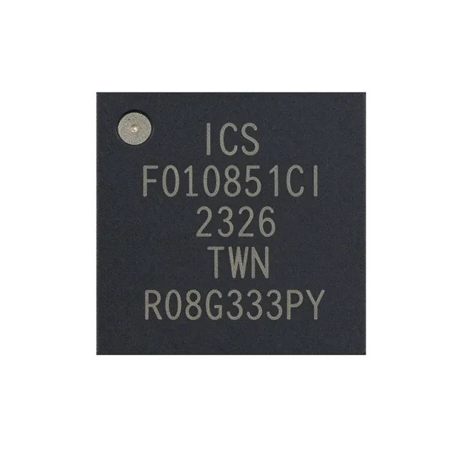
What Is the Renesas 9FGL0851CKILF and Why Do Server Designers Use It?
The 9FGL0851CKILF is the 8-output member of the Renesas 9FGL02x1 / 04x1 / 06x1 / 08x1 PCIe clock generator family. It is a PLL-based frequency synthesizer: an internal PLL multiplies the 25 MHz fundamental reference to the 100 MHz PCIe base rate, and per-output dividers and HCSL drivers distribute eight differential pairs. Renesas designed it to replace a discrete fanout buffer plus resistor termination network on server and high-performance computing boards, and the integrated termination is the headline feature.
Each HCSL output supports both 100 ohm termination (standard PCIe) and 85 ohm termination (mobile PCIe and specific OEM platforms), selected by the TERM_SEL strap on pin 38. With on-die resistors, you remove four external components per output — 32 components on an 8-output design — which shrinks the keep-out zone near chipset and switch BGA packages where routing external resistor pairs is impractical.
The output count maps directly onto a typical server clock tree: one CPU root complex, a downstream PCIe switch uplink, and 2-3 NVMe or NIC endpoints. Because the part supports CC, SRNS, and SRIS architectures per the PCIe Base Specification, it covers the Separate Reference No Spread and Separate Reference Independent Spread schemes that Gen 4 and Gen 5 platforms require.
Takeaway: If your board needs eight PCIe HCSL pairs from one 25 MHz reference and you want to cut 32 termination resistors, this device was purpose-built for exactly that topology.
How Do You Design In the 9FGL0851CKILF? Layout, Power, and Strapping Guide
Design-in follows three areas: reference routing, power architecture, and output termination.
Reference routing. Place the 25 MHz crystal or clock source within 200 mils of the REF_IN pin (pin 1) to minimize reference jitter. Keep the reference return path on REF_GND (pin 2) clean and local.
Power architecture. The core runs from 3.3 V on the VDD pins (3, 12, 28, 41). The optional VDDIO rail (pins 4 and 20) accepts 1.05 V and saves approximately 35% power versus running the outputs at 3.3 V — worthwhile on boards that already have a 1.05 V low-voltage rail shared with memory and chipset silicon. Place the device on the same 3.3 V plane as the chipset PCIe clock tree. Typical power consumption is 112-206 mW at 3.3 V depending on output loading, so no dedicated thermal solution is needed; the 7x7 mm VFQFPN dissipates this adjacent to an accelerator ASIC without concern.
Output termination. Set TERM_SEL (pin 38) for 100 ohm (standard PCIe slots and PHYs) or 85 ohm (mobile-derived OEM silicon). The datasheet reference design guideline is 5 inches total trace length; only add the 33 ohm series resistors on each HCSL output to dampen reflections if your layout exceeds that guideline.
Spread spectrum and power gating. Configure down-spread via the SS_SEL0 (pin 36) and SS_SEL1 (pin 37) strapping pins: spread off, 0.25%, or 0.5%. Down-spread reduces EMI peak energy, which helps dense server and NAND storage boards pass radiated emissions without additional shielding. Each output has its own active-low OE# pin (OE0# through OE7#), CLKREQ#-compatible, so firmware or the chipset can gate idle PCIe links individually — critical for server platforms managing slot power.
Package and grounding. The 48-VFQFPN follows JEDEC MO-220. Pin 48 is not connected on the die side but the exposed pad connects to GND internally, so solder the exposed pad to the board ground plane for the lowest-inductance return.
Takeaway: Keep the 25 MHz reference within 200 mils, use VDDIO at 1.05 V when a low-voltage rail exists for a ~35% power cut, and skip external series resistors unless traces exceed the 5-inch reference guideline.
What Are the Key Pins of the 9FGL0851CKILF? (48-VFQFPN Pinout Highlights)
The full 48-pin table lives on the 9FGL0851CKILF product page, but the functionally critical pins are: pin 1 REF_IN (25 MHz fundamental reference input), pin 3 VDD (3.3 V core), pin 4 VDDIO (1.05 V optional output supply), pins 6/7 OUT0_P/OUT0_N through pins 33/34 OUT7_P/OUT7_N (the eight HCSL differential pairs), the eight active-low OE# pins (8, 11, 16, 19, 24, 27, 32, 35), pins 36/37 SS_SEL0/SS_SEL1 (spread spectrum strapping), pin 38 TERM_SEL (100/85 ohm termination select), and the GND/NC pins including pin 48 with its internally grounded exposed pad. Pin 1 orientation follows standard QFN top-left convention.
Takeaway: Verify the three strap pins (SS_SEL0, SS_SEL1, TERM_SEL) against your schematic before tape-out — they define EMI behavior and termination impedance with no firmware recovery path.
What Are the Best Drop-In Alternatives to the 9FGL0851CKILF?
The verified drop-in alternatives are all same-family Renesas parts sharing the 48-VFQFPN (KILF) footprint. A cross-brand (TI or Diodes Inc.) drop-in equivalent was not confirmed in the verified cross-reference data; functionally similar PCIe Gen 5 clock generators from those vendors use different package pinouts and are not pin-compatible. For drop-in replacement, stay within the 9FGL family.
| Parameter | 9FGL0851CKILF | 9FGL0851BKILF | 9FGL0841AKILF | 9FGL0651BKILF | 9FGL0451BKILF | 9FGL0841CKILF |
|---|---|---|---|---|---|---|
| Package / footprint | 48-VFQFPN (KILF), 7x7 mm | Same VQFN-48 KILF footprint and pinout | Same footprint | Smaller package | Smaller package | Same footprint |
| Output count | 8 | 8 | 8 | 6 | 4 | 8 |
| PCIe generation support | Gen 1-5 | Gen 1-6 (backward compatible to Gen 1-5) | Gen 1-4 only | [Sibling of Gen 6-capable B revision family] | [Sibling of Gen 6-capable B revision family] | Gen 1-5 only, no Gen 6 |
| VDD / VDDIO scheme | 3.3 V core, 1.05 V optional | Same | Not stated in verified data | Same VDD/VDDIO scheme | Same VDD/VDDIO scheme | Not stated in verified data |
| Role vs. 9FGL0851CKILF | Base part | Recommended replacement; adds Gen 6 | Older revision register | 6-output sibling | 4-output sibling | Alternative same-footprint 8-output part |
For Gen 6 platforms or new designs, the 9FGL0851BKILF is the clear choice: same footprint and pinout, adds Gen 6, backward compatible. The only design impact is firmware-side verification of the new revision identifier register — no PCB rework or BOM changes. The 9FGL0841BKILFT (available on the XAIPART MPN list) is also drop-in compatible if Gen 6 is not required. Note per the family datasheet that 9FGL0851 and 9FGL0841 differ in spread spectrum default settings; both are pin-compatible in the 48-VFQFPN. Where fewer outputs suffice, the 9FGL0651BKILF (6 outputs) and 9FGL0451BKILF (4 outputs) keep the same VDD/VDDIO scheme in smaller packages.
Takeaway: Standardize new designs on the 9FGL0851BKILF; use 9FGL0841-family parts for last-time-buy coverage on Gen 1-5 platforms.
What Is the Lifecycle and Supply Situation for the 9FGL0851CKILF?
Two verified sources report different lifecycle states, and buyers should understand both:
- XAIPART database: Active. The part is listed with 16,870 units in stock, MOQ 1, tiered pricing from $8.1563 (qty 1) through $5.8906 (qty 10), $5.2109 (qty 100), $4.9844 (qty 500), and $4.7578 (qty 1000) as of 2026-11-02.
- Renesas product page: Obsolete. Verified 2026-10-06, the manufacturer marks the 9FGL0851CKILF Obsolete; samples are no longer orderable directly, and Renesas recommends the 9FGL0851BKILF or the 9FGL0841 family (both PCIe Gen 1-6 capable) for active designs. Distributor listings tracked via Octopart show 5 distributors, LCSC at approximately $5.00 per unit as of 2026-10-06, and Components-House listing 4009 pieces in stock. Bulk distributor pricing ranges approximately $4.50 at qty 10 down to roughly $2.98 at qty 1000 depending on date code and inventory depth — note these distributor figures differ from XAIPART's verified tiered pricing above, and both are cited as published.
The practical reading: this is last-time-buy territory. Factory lead time no longer exists, so above a few hundred pieces, confirm stock depth, date code, and RoHS traceability case-by-case with the distributor. Existing stock may command a premium over original MSRP as channels deplete.
Takeaway: If you must keep the C-version in an existing BOM, buy your full program volume now and qualify the 9FGL0851BKILF as the forward fit in parallel.
What Should Buyers and Designers Watch Next for PCIe Clocking?
Three trends anchored to the verified specs:
1. Gen 6 migration. The C-version tops out at PCIe Gen 5 (PCI Express Base Specification Rev 5.0 compliance). The recommended replacement, 9FGL0851BKILF, extends to Gen 6 in the same footprint. Any new PCB should drop in the B-version now so a future Gen 6 platform upgrade needs no respin.
2. SRIS as the default for multi-root platforms. The device's support for CC, SRNS, and SRIS architectures reflects where Gen 4/Gen 5 platforms have moved: separate reference clocks with independent spread. Verify your platform's required architecture against the strap configuration before committing a design.
3. Low-voltage I/O rails. The 1.05 V VDDIO option delivering ~35% power savings signals the direction of platform design: clock ICs sharing low-voltage rails with memory and chipset silicon. On thermally constrained M.2 and U.2 form factors, that power delta is a design input, not an afterthought.
Takeaway: Design new boards around the Gen 6-capable B-version, use SRIS-compatible strapping, and exploit the 1.05 V VDDIO rail wherever the platform provides it.
Where Should You Buy the 9FGL0851CKILF?
XAIPART lists 9FGL0851CKILF with 16,870 units in stock, MOQ 1, and tiered pricing as of 2026-11-02 ($8.1563 at qty 1; $5.8906 at qty 10; $5.2109 at qty 100; $4.9844 at qty 500; $4.7578 at qty 1000). The full family datasheet (9FGL02x1-04x1-06x1-08x1, 37 pages, free Renesas login for the latest revision) is available from the official Renesas product page. For broader component sourcing across clock and timing ICs, browse the XAIPART component catalog, and for more engineering deep-dives see the XAIPART blog — including guides such as the ATMXT336S-CCUR maXTouch controller guide for comparable spec-and-sourcing treatment of other interface ICs.
Takeaway: Order volume from XAIPART stock while it lasts, verify date codes given the obsolete manufacturer status, and line up the 9FGL0851BKILF as the successor.
কমেন্ট
প্রথম কমেন্ট দিন
🔐 অনুরোধ করুন সাইন ইন মন্তব্য পোস্ট করার জন্য
অ্যাকাউন্ট নেই? সাইন আপ