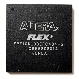
LFE2-50E-6F484C - 48K LUT ECP2 FPGA | Lattice
MPN: LFE2-50E-6F484C ✓ সক্রিয়LFE2-50E-6F484C সারাংশ
An FPGA is a programmable semiconductor whose digital logic, interconnect, and I/O behavior are defined after fabrication through a configuration bitstream. Within the product hierarchy, the LFE2-50E-6F484C is a field-programmable gate array, specifically a member of the Lattice ECP2 family and the broader integrated-circuit and semiconductor categories. Compared with a fixed-function ASIC, it permits design revisions, field updates, and adaptation to multiple hardware configurations without changing the PCB.
Key features include a nominal 50,000-cell FPGA implementation, 6,000 LUTs, and 396,288 bits of distributed RAM. The device provides 339 user I/O according to distributor listings, making the 484-ball package suitable for designs that need more external connections than a smaller FPGA can offer. Its 1.2 V operating class supports low-voltage digital systems, while the -6 ordering code identifies the device's performance grade.
The ECP2 architecture is intended to combine programmable logic with embedded memory resources in a single package. Distributed RAM can be used for buffers, lookup functions, small state machines, and data transformations without requiring external memory for every small storage requirement. The available verified sources do not state the exact number of DSP blocks, PLL count, supported I/O standards, maximum clock frequency, or internal memory organization, so these values must be confirmed in the manufacturer datasheet before design release.
Typical uses include industrial automation, test and measurement, communications interfaces, embedded control, video or display control, and general-purpose signal processing. The large I/O count is particularly useful when a design must bridge multiple buses, converters, memories, LEDs, connectors, and communication transceivers while retaining a reconfigurable logic fabric.
Designers should confirm power sequencing, decoupling, configuration interface requirements, ball assignments, and high-speed layout constraints against the official LatticeECP2/M family data sheet. Because the supplied web results do not expose a complete 484-ball pin map, the package drawing should not be inferred from a generic BGA layout.
This page consolidates the verified distributor specifications, family-level substitute information, application guidance, and design cautions so engineers can compare the LFE2-50E-6F484C against pin-compatible ECP2 options without treating package similarity as proof of complete interchangeability.
এর জন্য ড্রপ-ইন বিকল্প LFE2-50E-6F484C — একই package, pin-to-pin compatible। ভিন্ন package-এর যেসব পার্টে PCB rework প্রয়োজন সেগুলো বাদ দেওয়া হয়েছে।
LFE2-50E-6FN484C
✅ ড্রপ-ইন📋 রেফারেন্স বিকল্প (ক্যাটালগে নেই)
LFE2-50E-6FN484I
✅ ড্রপ-ইন📋 রেফারেন্স বিকল্প (ক্যাটালগে নেই)
LFE2-50SE-7FN484C
✅ ড্রপ-ইন📋 রেফারেন্স বিকল্প (ক্যাটালগে নেই)
LFE2-50E-5F484C
✅ ড্রপ-ইন📋 রেফারেন্স বিকল্প (ক্যাটালগে নেই)
LFE2-35SE-6F484C
✅ ড্রপ-ইন📋 রেফারেন্স বিকল্প (ক্যাটালগে নেই)
LFE2-50E-6F484C সর্বোচ্চ রেটিং ও বৈদ্যুতিক বৈশিষ্ট্য
| Device Type | ECP2 field-programmable gate array (FPGA) |
| Logic Elements | 48,000 logic elements |
| Lookup Tables | 6,000 LUTs |
| Nominal Cell Count | 50,000 cells |
| Distributed RAM | 396,288 bits |
| Maximum User I/O | 339 I/O |
| Core Supply Voltage | 1.14 V to 1.26 V |
| Nominal Operating Voltage | 1.2 V |
| Speed Grade | -6 |
| প্যাকেজ | 484-BBGA |
| Package Form | Square BGA |
| Terminal Count | 484 terminals |
| মাউন্টিং টাইপ | Surface mount |
| DSP Capability | DSP-equipped ECP2 FPGA |
LFE2-50E-6F484C square bga পিন কনফিগারেশন গাইড
LFE2-50E-6F484C (square bga প্যাকেজ)-এর পিন কনফিগারেশন। এই ডিজিটাল IC-তে GPIO, কমিউনিকেশন ইন্টারফেস (UART, SPI, I2C) এবং পাওয়ার পিন রয়েছে। বিকল্প পিন ফাংশন ও কনফিগারেশন অপশনের জন্য প্রস্তুতকারকের ডেটাশিট দেখুন। এমবেডেড সিস্টেম ডিজাইন ও PCB লেআউটের জন্য অপরিহার্য।

এর জন্য বিস্তারিত পিনআউট ডেটা পাওয়া যায়নি LFE2-50E-6F484C.
দেখুন ডেটাশিট সম্পূর্ণ পিন কনফিগারেশনের জন্য।
সাধারণ ব্যবহার
LFE2-50E-6F484C এর জন্য উপযুক্ত 6 অ্যাপ্লিকেশনs: Industrial Automation Controller, Communications Interface Gateway, Test and Measurement Instrumentation, Embedded System Control Hub, Display and Video Interface Controller, Programmable Signal Processing.
Industrial Automation Controller
The LFE2-50E-6F484C fits industrial automation when a controller needs substantial programmable logic and a large connector count. Its 6,000 LUTs and 396,288 bits of distributed RAM can support state machines, sequencing logic, interface translation, and local data buffering, while up to 339 user I/O can connect field inputs, outputs, communications transceivers, and status indicators. The 1.14 V to 1.26 V operating range suits low-voltage digital designs. Before deployment, verify the exact temperature grade, I/O standards, isolation requirements, and industrial compliance expectations in the manufacturer documentation because those details are not present in the supplied snippets.
সুপারিশকৃত
Communications Interface Gateway
The LFE2-50E-6F484C can implement protocol conversion, packet framing, buffering, and interface bridging in communications equipment. The device combines 48,000 logic elements with 396,288 bits of distributed RAM, providing enough distributed resources for multiple finite-state machines and line-buffer functions without making external RAM the only option for small working sets. Its 339 user I/O are useful for parallel buses and control signals. The -6 speed grade should be checked against the required clock and timing margins, and all I/O voltage standards must be confirmed directly from the ECP2 family data sheet.
সুপারিশকৃত
Test and Measurement Instrumentation
The LFE2-50E-6F484C is suitable for programmable test and measurement front ends that combine timing, control, and data-acquisition functions. Its 48,000 logic elements can implement sequencers, pattern generators, counters, acquisition control, and interface logic, while the 396,288-bit distributed RAM can support compact buffers and lookup data. A high count of 339 user I/O allows connection to sensors, ADC interfaces, relay drivers, displays, and test fixtures through the 484-BBGA package. Timing closure remains critical in high-speed instrumentation, so engineers should verify clocking resources, pin standards, output slew behavior, and configuration requirements in the official documentation.
সুপারিশকৃত
Embedded System Control Hub
The LFE2-50E-6F484C can serve as the programmable control hub in an embedded system that needs more parallel I/O and dedicated logic than a microcontroller provides. The device can implement hardware-assisted control, peripheral bridges, dedicated timing, and state management while a microcontroller executes higher-level software. Its 6,000 LUTs and 396,288 bits of distributed RAM make it appropriate for fixed datapaths and local buffering, and the 339 user I/O simplify connections among sensors, converters, memory, and external transceivers. The system designer must confirm startup configuration behavior, I/O-bank voltage limits, and reset architecture before committing the FPGA to a critical control path.
সুপারিশকৃত
Display and Video Interface Controller
The LFE2-50E-6F484C is appropriate for display, monitor, and video interface designs requiring flexible timing and multiple control outputs. Its programmable logic can generate pixel and timing signals, translate interface formats, and coordinate data paths, while 396,288 bits of distributed RAM can support compact line or frame data structures. The 339 user I/O provide capacity for display-control signals and companion interface devices. However, the supplied sources do not specify supported DVI or HDMI interfaces, PLL quantities, or maximum video timing, so those capabilities should not be assumed; consult the ECP2 family data sheet and validate the selected display PHY externally.
সুপারিশকৃত
Programmable Signal Processing
The LFE2-50E-6F484C can implement parallel signal-processing pipelines where deterministic hardware operation, reusable logic, and high I/O density are important. Its 6,000 LUTs can support filters, correlators, packetizers, and digital state machines, while the ECP2 family's DSP capability supports higher-density arithmetic pipelines when the required blocks and throughput are confirmed. The -6 speed grade provides a defined performance class, and 339 user I/O suit parallel data acquisition and control. Verify the exact DSP-block count, supported clock frequencies, and I/O timing in the manufacturer data sheet before using this device for a timing-critical DSP replacement.
সুপারিশকৃত
সুপারিশকৃত পণ্যের সারসংক্ষেপ
এর জন্য ইঞ্জিনিয়ারিং রেফারেন্স ডেটা LFE2-50E-6F484C — তুলনা, ডিজাইন গাইডেন্স এবং কমপ্লায়েন্স তথ্য।
নির্বাচন গাইড
বিকল্পের সাথে তুলনা
| পারামিটার | এই পণ্য | LFE2-50E-6FN484C | LFE2-50E-6FN484I | LFE2-50SE-7FN484C | LFE2-50E-5F484C | LFE2-35SE-6F484C |
|---|---|---|---|---|---|---|
| Package | 484-BBGA | 484-BBGA - same | 484-BBGA - same | FPBGA-484 - same package class | 484-pin FBGA - same package class | 484-BBGA - same |
| Brand | Lattice Semiconductor | Lattice Semiconductor | Lattice Semiconductor | Lattice Semiconductor | Lattice Semiconductor | Lattice Semiconductor |
| Device Family | Lattice ECP2 | Lattice ECP2 | Lattice ECP2 | Lattice ECP2 | Lattice ECP2 | Lattice ECP2 |
| Speed Grade | -6 | -6 | -6 | -7 | -5 | -6 |
মূল পার্থক্যসমূহ
- Directly matches the verified -6 ECP2 configuration (বনামLFE2-50E-5F484C)
- Provides 48,000 logic elements and 6,000 LUTs with 339 I/O (বনামLFE2-35SE-6F484C)
- Provides a documented 1.14 V to 1.26 V core-supply range (বনামLFE2-50SE-7FN484C)
- Combines 396,288 bits of distributed RAM with 339 user I/O (বনামLFE2-50E-6FN484C)
ডিজাইন নোট
Do not treat any 484-BBGA ECP2 device as automatically interchangeable merely because the package has the same ball count. The verified comparison source warns that family membership does not establish pin compatibility, and ordering suffixes can encode speed, temperature, qualification, or other device characteristics. Before substitution, compare the manufacturer ball tables, configuration pins, I/O-bank requirements, power rails, and speed-grade timing. This is particularly important for LFE2-50E-6FN484C and LFE2-50E-5F484C, whose ordering codes differ from the target.
Plan the 1.14 V to 1.26 V core rail and any required I/O rails as separate power-design problems. The supplied snippets do not identify the number of voltage domains, current limits, sequencing order, or configuration-supply requirements, so these values must be taken from the official family data sheet. Place local high-frequency decoupling at the supply and ground balls indicated by the reference layout, preserve the required plane connectivity, and verify startup behavior across the complete -6 speed-grade operating range before releasing the PCB.
A 484-ball BGA requires a package-specific escape strategy, and the verified data does not include the complete ball map. Create the PCB footprint from the manufacturer package drawing rather than from a generic BGA land pattern, and assign every ball to power, ground, configuration, user I/O, or a documented no-connect function. Confirm pad-stack dimensions, solder-mask definition, via-in-pad policy, and assembly X-ray requirements with the package drawing and the board fabricator before high-volume production.
Use the -6 timing grade as a constraint, not as a substitute for interface analysis. For each high-speed interface, verify input and output timing, clock quality, voltage standards, skew, and termination requirements against the manufacturer data sheet. If the design uses differential pairs, route them as controlled-impedance nets over a continuous reference plane and avoid splits or unnecessary stubs. The verified sources do not identify the supported I/O standards or maximum clocks, so do not infer them from the generic ECP2 family description.
Verify configuration startup, bitstream generation, and system initialization before schematic sign-off. A valid FPGA bitstream must match the exact device, speed grade, package, configuration mode, and any application-specific features, so moving from the LFE2-50E-6F484C to a -5, -7, or differently suffixed candidate can require a new programming file. Include a reliable configuration source and recovery path in the architecture, and use the manufacturer-supported toolchain and device database corresponding to the selected part.
কমপ্লায়েন্স তথ্য
The verified FindIC comparison describes LFE2-50E-5F484C as lead-free, but no explicit RoHS, REACH, halogen-free, conflict-minerals, or AEC-Q100 declaration for the target was supplied. The target is an FPGA rather than an automotive-qualified device in the provided data.