Amplifier ICs
Products (796)

LMV344QIPWRQ1 - Quad 1MHz Rail-to-Rail Op-Amp | TI Automotive
The Texas Instruments LMV344QIPWRQ1 is an automotive-grade (AEC-Q100), quad-channel CMOS operational amplifier delivering 1 MHz gain-bandwidth and 75 mA of high output current from a single 2.7 V to 5.5 V supply, packaged in a 14-pin TSSOP (PW) for surface-mount assembly. An operational amplifier is a high-gain DC-coupled voltage amplifier that, with external feedback networks, performs signal amplification, buffering, filtering, and comparison functions. Within the power-management hierarchy, the LMV344 belongs to the general-purpose low-voltage op-amp family (LMV341/LMV342/LMV344 single/dual/quad), itself a subset of CMOS amplifiers within the broader analog signal-chain category. Key features include rail-to-rail output swing, which maximizes dynamic range on low-voltage 3.3 V and 5 V rails; 75 mA output current capability, roughly 10x a general-purpose op amp, enabling direct driving of low-impedance loads such as ADC inputs, capacitive loads through isolation resistors, and transmission lines; and operation up to 125C ambient, supporting under-hood and body-electronics environments. The quad configuration saves board space and BOM cost versus four single-channel devices. The CMOS input architecture provides low input bias current and low quiescent power, while the rail-to-rail output stage minimizes headroom losses near the supply rails. The -Q1 suffix denotes AEC-Q100 qualification and PPAP support for automotive production, distinguishing it from the commercial LMV344. Typical applications include automotive sensor signal conditioning, battery-current and voltage monitoring front ends, driving ADCs in body-control modules, LED indicator drivers, and audio buffers in instrument clusters. The 75 mA drive also suits speaker or actuator buffer duties at low frequencies. Design tip: with 75 mA drive capability, verify power dissipation in the small TSSOP-14 package when sourcing high current continuously, and add an isolation resistor (10-50 ohm) when driving large capacitive loads to preserve phase margin. Pricing references are as of 2026-08-29.
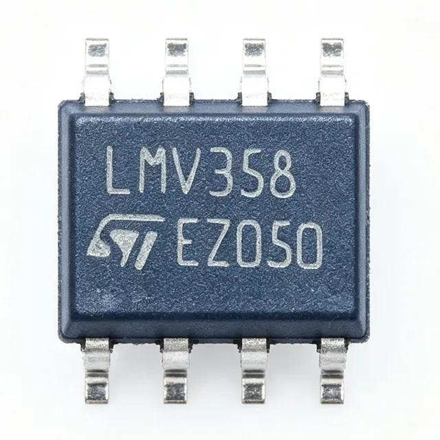
LMV358IDT - Dual Low-Power Op Amp | STMicroelectronics
The LMV358IDT is a dual low-power operational amplifier from STMicroelectronics, designed for battery-powered and portable applications. It operates from a single supply voltage ranging from 2.7V to 5.5V, with a typical quiescent current of 210 µA per amplifier. The device is offered in the SOIC-8 package, making it suitable for space-constrained designs. Data verified as of 2026-08-05. An operational amplifier (op amp) is a high-gain voltage amplifier with differential inputs and a single-ended output. It is a fundamental building block in analog electronics, used in signal conditioning, filtering, and amplification tasks. The LMV358IDT belongs to the low-power op amp category, which prioritizes minimal power consumption for battery-operated devices. In the hierarchy of analog components, it sits under linear ICs, which are part of the broader integrated circuits family. Key features of the LMV358IDT include a low supply current of 210 µA per channel, a wide supply voltage range of 2.7V to 5.5V, and a rail-to-rail output stage that swings within 10 mV of the supply rails. The input common-mode voltage range extends to ground, allowing single-supply operation. The device also features a gain bandwidth product of 1.3 MHz and a slew rate of 0.45 V/µs, sufficient for audio and sensor signal conditioning. The LMV358IDT uses a bipolar technology with a class-AB output stage, providing low crossover distortion. The input stage is a PNP transistor pair, enabling the input common-mode range to include ground. The output stage can source and sink current, with a short-circuit current of 160 mA. The device is internally frequency compensated for unity-gain stability, simplifying design. Typical applications include battery-powered instrumentation, portable medical devices, sensor signal conditioning, and active filters. The low quiescent current extends battery life, while the rail-to-rail output maximizes dynamic range in single-supply systems. The wide supply range also allows operation from 3.3V or 5V logic rails. When designing with the LMV358IDT, ensure proper decoupling with a 0.1 µF capacitor close to the supply pin. The input common-mode range includes ground, but for best performance, keep inputs within the specified range. The output can drive capacitive loads up to 100 pF without oscillation, but larger loads may require a series resistor. This page synthesizes distributor pricing, drop-in alternatives, and practical design notes not found in the STMicroelectronics datasheet, providing a comprehensive resource for engineers.

LMV358SG-13 - Dual 1MHz Rail-to-Rail Op Amp, 8-SO | Diodes Inc
The Diodes Incorporated LMV358SG-13 is a dual-channel, low-voltage, rail-to-rail output operational amplifier supplied in an 8-pin SOIC package and shipped on 13-inch reel packaging. Per the manufacturer datasheet, the part provides a 1 MHz gain-bandwidth product, a 1 V/µs typical slew rate, and operates from a single 2.7 V to 5.5 V supply, targeting general-purpose and cost-sensitive analog designs. A rail-to-rail output operational amplifier is a type of operational amplifier (OP-Amp) whose output voltage can approach both supply rails, unlike traditional amplifier topologies whose swing is limited to 1.5-2 V below each rail. Within the broader hierarchy, this device belongs to the linear amplifier family, which sits under integrated circuits and power management/analog signal chain categories. Rail-to-rail capability enables designs to maximize dynamic range in low-voltage single-supply systems such as battery-powered portable equipment. Key features include a 1 MHz gain-bandwidth product, 1 V/µs slew rate, low-voltage 2.7 V to 5.5 V single-supply operation, and CMOS input architecture suitable for general-purpose signal conditioning. The LMV321/LMV358/LMV324 family from which this part derives was designed to effectively reduce cost and footprint at low voltage levels, with the SG-13 suffix indicating 8-SOIC package and 13-inch reel quantity. This makes the part especially attractive for high-volume consumer and industrial designs. Internally the device uses CMOS input stages that support low input bias current and a common-mode range that includes the negative rail, while the output stage is designed to swing within millivolts of either rail. Compared with bipolar-input rail-to-rail op amps, the LMV358 family typically delivers lower input bias current at the cost of slightly higher input-referred voltage noise. Typical applications include portable consumer electronics, battery-powered sensor interfaces, signal conditioning for ADC front-ends, general-purpose active filters, headphone driver stages, and transducer pre-amplification. The dual-channel configuration allows space-efficient implementation of difference amplifiers, instrumentation front-ends, or dual-pole Sallen-Key filters. When designing with this part, ensure input common-mode voltage stays within the specified range, place a 0.1 µF decoupling capacitor close to the supply pin, and verify output drive capability against the load. The rail-to-rail output stage requires minimum output current loading to maintain linearity near the rails. This page synthesizes distributor pricing, drop-in alternatives, and practical design notes not found in the manufacturer datasheet, giving a more complete engineering reference for component selection.

LMV761MFX/NOPB - 120ns Precision Comparator w/ Shutdown | TI | SOT-23-6
The Texas Instruments LMV761MFX/NOPB is a single-channel, 120-ns, low-voltage precision comparator with shutdown and a push-pull output stage, housed in a 6-pin SOT-23 (DBV) package. It operates from a 2.7 V to 5 V single supply, draws a typical quiescent current well below 1 mA in active mode, and integrates a SHDN pin that drops supply current to a sub-microampere level when pulled low. The part is specified over the -40C to +125C industrial temperature range and is lead-free / RoHS compliant (NOPB suffix). A comparator is a high-gain differential amplifier whose output swings fully high or fully low depending on which of its two inputs is more positive. Precision comparators such as the LMV761 are distinguished from general-purpose comparators by very low input offset voltage, low input bias current, and tight propagation delay, making them the reference building block for threshold detection, zero-crossing detection, and analog signal conditioning. The LMV761 belongs to the linear / comparator IC category, sits in the signal-chain hierarchy between analog front-ends and digital logic, and is widely used in battery-powered and space-constrained designs. Key features of the LMV761MFX/NOPB include a 120 ns typical propagation delay, push-pull CMOS output (no pull-up resistor required), rail-to-rail input common-mode range, an active-low shutdown pin for power management, internal hysteresis for clean switching on slow signals, and ESD protection on the pins. The push-pull topology drives CMOS/TTL loads directly with symmetric rise/fall times, which is critical when the comparator output feeds a high-impedance logic input or a microcontroller interrupt. Architecturally, the LMV761 uses a bipolar-CMOS input stage that yields low input bias current combined with low offset, followed by a fast latch and CMOS output drivers. The shutdown circuit is implemented as a gated bias path that collapses the input stage current when SHDN is low, while preserving the output in a defined high-impedance state so downstream circuitry can hold the last logic level. Typical applications include battery management (over-voltage / under-voltage detection), threshold detectors in industrial sensor modules, line drivers and zero-crossing detectors for power-line monitoring, alarm and security subsystems, and general signal conditioning ahead of an MCU ADC. Designers favor it for any 3.3 V or 5 V system that needs a fast, low-power, board-space-saving comparator. When designing with this part, place a 0.1 uF bypass capacitor within a few millimeters of VCC, keep input trace lengths short to minimize parasitic feedback that causes oscillation, and ensure the SHDN pin (when unused) is tied high through a resistor, never left floating. The push-pull output cannot be wire-ORed with another comparator output; if that topology is required, select an open-drain variant instead. This page synthesizes distributor pricing, drop-in same-package alternatives, comparison parameters, and practical PCB-level design notes that complement the manufacturer datasheet without replacing it.

LMV841MGX/NOPB - 4.5MHz RRIO CMOS Op-Amp, SC-70-5 | TI
The Texas Instruments LMV841MGX/NOPB is a single-channel CMOS input, rail-to-rail input and output (RRIO), low-power operational amplifier that operates over a wide 2.7 V to 12 V supply range. The device is housed in a space-saving 5-pin SOT-SC70 (DCK) package and offers 4.5 MHz unity-gain bandwidth, low offset voltage, and a CMOS input stage. According to the manufacturer datasheet, the LMV84x family is optimized for high-impedance sensor interfaces and battery-powered applications. A CMOS-input op-amp (operational amplifier) is a linear amplifier whose input stage is built using CMOS transistors rather than bipolar junction transistors. CMOS inputs provide extremely high input impedance (very low bias current), making them ideal for interfacing with high-impedance sensors such as photodiodes, electrochemical cells, and piezoelectric transducers. Rail-to-rail input and output (RRIO) capability allows the input common-mode signal and the output swing to reach within millivolts of both supply rails, maximizing dynamic range when operating from low-voltage supplies. These characteristics position the LMV841 within the broader hierarchy of operational amplifier -> amplifier IC -> analog signal chain -> integrated circuit. Key features include a 4.5 MHz gain-bandwidth product, low input bias current due to the CMOS input stage, rail-to-rail input and output swing, low supply current consumption for battery operation, and operation from 2.7 V to 12 V single supply. The CMOS input stage virtually eliminates input bias current errors that would otherwise limit high-impedance sensor designs, while the RRIO capability preserves dynamic range in low-voltage single-supply systems. The 5-pin SC-70 package measures only 2.0 mm x 1.25 mm, enabling high-density analog front-end designs. Typical applications include battery-powered instrumentation, photodiode transimpedance amplifiers, handheld medical devices, sensor signal conditioning, active filters, and portable audio signal chains. The wide supply range allows direct interfacing to lithium-ion cells (3.6 V nominal, 4.2 V peak) as well as 9 V industrial rails without level shifting. When designing with the LMV841, place a 0.1 uF decoupling capacitor within 5 mm of the supply pin to minimize noise coupling. Avoid placing large resistive loads directly at the output when operating near the rails, as the output drive capability degrades within approximately 50 mV of either rail under heavy loading. This page consolidates distributor stock and pricing data, drop-in alternative part numbers in the same SC-70-5 footprint, and practical SC-70 PCB layout guidance that augments the manufacturer datasheet for accelerated component selection.

LMV932MMX/NOPB - Dual 1.8V RRIO Op Amp 1.5MHz | TI
The Texas Instruments LMV932MMX/NOPB is a dual low-voltage, low-power operational amplifier from the LMV93x-N family, operating from a 1.8V to 5.5V supply with rail-to-rail input and output (RRIO) performance in a space-saving 8-pin VSSOP package. It provides 1.5MHz gain-bandwidth and can source up to 5mA of output current, making it well suited to battery-powered and portable signal conditioning. An operational amplifier (op amp) is a high-gain voltage amplifier with differential inputs and a single-ended output, the fundamental building block of analog signal chains. Within the power-management hierarchy of a system, general-purpose op amps such as this one sit between sensors and ADCs, performing amplification, filtering, buffering, and level shifting. The LMV93x-N family spans a single (LMV931-N), dual (LMV932-N), and quad (LMV934-N) to cover channel-count scaling. Key features include guaranteed operation down to 1.8V for single-cell Li-Ion or two-cell alkaline end-of-life conditions, rail-to-rail input common-mode that extends to both supply rails, and rail-to-rail output swing that maximizes dynamic range at low supply voltages. The NOPB suffix confirms lead-free, RoHS-compliant packaging. Temperature range is -40C to +125C, and the MMX suffix denotes the VSSOP-8 (DGK) surface-mount package suited to area-constrained PCBs. The rail-to-rail input stage typically uses complementary PMOS/NMOS differential pairs to avoid common-mode crossover distortion near the rails, allowing sensor signals at or near ground or VCC to be processed accurately. The output stage swings within millivolts of the rails under light load, maximizing ADC input utilization at 1.8V operation. Typical applications include mobile phone and tablet audio or sensor front ends, battery-powered instrumentation, active filters in portable medical devices, and low-voltage ADC driver stages. The compact VSSOP footprint makes the part a good fit for dense multi-channel boards. Design consideration: at 1.8V supply, output current capability and headroom are limited; keep load impedances above several kilohms and verify bandwidth requirements, since 1.5MHz gain-bandwidth means closed-loop gains of 10 or more restrict usable signal bandwidth to well under 150kHz.
LT1001CD - Precision Op-Amp 8-SOIC | Texas Instruments
The Texas Instruments LT1001CD is a precision operational amplifier with industry-leading DC accuracy, supplied in an 8-pin SOIC (D) package. It features a maximum input offset voltage of 110 uV, a unity-gain bandwidth of 0.8 MHz, and a low offset voltage drift of 0.3 uV/C. The single-channel amplifier is built for instrumentation, precision signal conditioning, and industrial measurement front ends. A precision op-amp is a type of operational amplifier designed to minimize the input-referred errors (offset voltage, bias current, drift, and noise) that limit DC accuracy. In the system hierarchy, the LT1001CD sits at the precision tier of general-purpose amplifiers, above standard 741-class parts and below chopper-stabilized zero-drift amplifiers. It is the workhorse of 16-bit and lower data-acquisition front ends, weigh scales, strain-gauge bridges, and thermocouple conditioning circuits where 10-100 uV of error must be resolved over industrial temperature ranges. Key features of the LT1001CD include 110 uV maximum input offset voltage, 4 nA maximum input bias current, 102 dB minimum open-loop gain, and 0.3 uV/C offset voltage drift. The device operates from +/-3 V to +/-18 V dual supplies or 6 V to 36 V single supply. Its bipolar input stage supports true differential sensing across the full input common-mode range, including ground-referenced signals when operated from a single supply. The C-grade commercial temperature range is 0C to +70C. Architecturally, the LT1001CD uses a precision bipolar input stage with active bias compensation, allowing it to maintain low offset and bias current over temperature without chopper-induced switching artifacts. The internal compensation network is unity-gain stable, eliminating the need for external compensation capacitors. The result is a versatile amplifier that combines 741-class simplicity with significantly tighter DC specifications. Typical applications include precision weighing scales, strain-gauge and load-cell amplifiers, thermocouple and RTD signal conditioning, medical instrumentation front ends, 16-bit SAR ADC input buffers, industrial process-control analog inputs, and reference-voltage buffering for precision DACs. The 8-SOIC package is footprint-compatible with industry-standard dual op-amps, simplifying board reuse in legacy designs. When designing with the LT1001CD, take care to provide adequate supply decoupling (100 nF ceramic close to each supply pin) and route sensitive bias-current paths to avoid leakage. Optional pins 1 and 8 support external offset nulling via a 10 kOhm potentiometer; if unused, leave them open. The input common-mode range extends to the negative supply, making true ground sensing possible on a single rail. This page synthesizes distributor pricing, drop-in alternatives, and practical design notes not found in the manufacturer datasheet alone. The information is anchored to the official Analog Devices LT1001 datasheet and cross-checked against Rochester Electronics, DigiKey, and JAK Electronics stock data as of 2026-10-22.
LT1012CD - Precision Op Amp, 25µV Offset, 8-SOIC | Texas Instruments
The Texas Instruments LT1012CD is a precision operational amplifier featuring 25 µV input offset voltage, 40 pA input bias current, and 200 µV typical offset in an 8-pin SOIC package. Originally designed by Linear Technology and now produced by Texas Instruments and authorized partners, the LT1012CD delivers picoampere-level bias currents over the full -55°C to +125°C temperature range with extremely high common-mode and power supply rejection ratios. A precision operational amplifier (op-amp) is a high-gain DC-coupled electronic voltage amplifier with a differential input and, usually, a single-ended output. Precision op-amps are characterized by low input offset voltage, low input bias current, low noise, and high common-mode rejection ratio (CMRR), making them suitable for amplifying small signals from sensors, transducers, and high-impedance sources. The LT1012 belongs to the broader category of linear integrated circuits and is positioned as a universal precision op-amp that combines the low-bias performance of BIFET/JFET-input amplifiers with the low-offset and low-drift characteristics of precision bipolar designs. Key features of the LT1012CD include 200 µV maximum input offset voltage, 40 pA maximum input bias current, 0.2 V/µs typical slew rate, and the ability to deliver 5 mA of output current while maintaining a voltage gain of one million. The device operates over a wide supply range (typically ±2 V to ±20 V) and offers extremely high CMRR and PSRR, with practically unmeasurable warm-up drift, making it ideal for precision instrumentation. The LT1012CD uses Linear Technology's advanced bipolar process technology that achieves sub-picoampere bias currents through active bias-current cancellation, while the precision bandgap-based input stage provides the low offset and low drift. The amplifier is internally compensated, eliminating the need for external compensation components in most applications, simplifying PCB layout and reducing BOM cost. Typical applications include precision thermocouple amplification, strain-gauge and weigh-scale signal conditioning, medical instrumentation, high-impedance sensor buffers, precision integrators for analog computation, and battery-powered portable instrumentation where the LT1012 achieves precision operation on two Ni-Cad batteries with only 1 mW of power dissipation. When designing with the LT1012CD, note that its 0.2 V/µs slew rate makes it suitable for DC and low-frequency signals but inadequate for high-speed or wide-bandwidth applications. For those applications, a faster op-amp such as the LT1028 or OP-27 should be considered. Standard 8-SOIC layout conventions apply, with input pins (IN+, IN-) at pins 3 and 2, output at pin 6, and power pins at pins 7 (V+) and 4 (V-). This page synthesizes distributor pricing, drop-in alternatives, and practical design notes that go beyond the manufacturer datasheet to support fast engineering decisions.
LT1013CD - Dual Precision 1MHz Op Amp | Texas Instruments
The Texas Instruments LT1013CD is a low-power dual precision operational amplifier with a 4 V to 44 V supply range, 1 MHz gain-bandwidth product, 0.4 V/us slew rate, and two amplifiers in an 8-pin SOIC package. The device combines high gain, low noise, low supply current, and low-offset-voltage temperature coefficient in one circuit. According to the Texas Instruments product page, LT1013CD is the lead-free SOIC orderable version of the LT1013 family. An operational amplifier is an analog signal-processing semiconductor that uses high open-loop gain to amplify voltage differences accurately. Within the broader hierarchy, an operational amplifier is a linear amplifier, analog IC, and signal-conditioning component. The LT1013 fits precision instrumentation because its dual configuration supports common differential, summing, filtering, threshold, or transimpedance stages while reducing board area. Verified product information identifies high gain, low noise, low supply current, and a low-offset-voltage temperature coefficient as principal family characteristics. The device can operate from a single 5 V supply, has a common-mode input range that includes ground, and produces output swings to within a few millivolts of ground, as stated in the supplied comparison-source material. These properties are useful in battery-powered measurements where larger supply headroom would be inconvenient. The LT1013 family supports broad supply operation from 4 V to 44 V, allowing the same precision amplifier architecture to serve low-voltage instrumentation and higher-voltage industrial signal chains. Its 1 MHz gain-bandwidth product supports moderate-bandwidth closed-loop functions rather than high-speed waveform or communications applications. The 0.4 V/us slew rate likewise favors low-frequency precision conditioning over wideband pulse acquisition. Analog Devices lists battery-powered precision instrumentation, strain-gauge signal conditioners, thermocouple amplifiers, instrumentation amplifiers, 4 mA to 20 mA current-loop transmitters, multiple-limit threshold detection, and active filters as representative LT1013 applications. These uses benefit from dual-channel operation, low supply current, precision behavior, and the ability to work across single and split supplies. When designing with the LT1013CD, preserve the required bypass capacitance, maintain common-mode and output headroom, and confirm that closed-loop bandwidth matches the 1 MHz family characteristic. Check noise, offset, supply current, and common-mode limits against the actual precision requirements. Pricing shown for LCSC is $0.4097 as of 2026-10-22; other distributor prices and current stock must be confirmed at purchase. This page combines verified manufacturer and distributor information, packaging details, applications, pricing context, and engineering guidance. It also identifies which parameters remain unavailable in the supplied evidence instead of estimating them, enabling engineers to make a more defensible LT1013CD selection.

LT1013CP - Dual Precision Op Amp, 4-44V | Texas Instruments
The Texas Instruments LT1013CP is a dual precision operational amplifier featuring high gain, low supply current, low noise, and a low offset-voltage temperature coefficient, supplied in an 8-pin PDIP (P) package. It operates from a single 4V to 44V supply (or dual ±2V to ±22V supplies), draws only 0.5 mA typical supply current per amplifier, and delivers 150 µV maximum input offset voltage at 25°C (LT1013A grade). The input common-mode range includes ground and the output swings to within a few millivolts of ground while sinking current, eliminating crossover distortion. A dual precision op amp is a two-channel integrated operational amplifier that combines matched transistor pairs and laser-trimmed thin-film resistors to achieve DC accuracy comparable to chopper-stabilized designs while consuming milliwatts of power. Within the broader component taxonomy, dual op amps sit under operational amplifiers -> amplifiers -> analog ICs -> semiconductor. The LT1013 was the first precision dual op amp in the 8-pin industry-standard pinout, upgrading legacy devices such as the MC1458/MC1558, LM158, and OP-221 with significantly lower noise and better DC stability. Key features include 150 µV max input offset voltage (LT1013A) with 2.5 µV/°C max offset voltage temperature coefficient, 0.5 mA typical supply current per amplifier, single-supply operation from 4V to 44V, ground-sensing input range, and output swing to within millivolts of ground. The NPN input stage delivers low input bias current and low voltage noise density suitable for transducer and instrumentation front-ends. Typical applications include battery-powered precision instrumentation, strain-gauge signal conditioners, thermocouple amplifiers, 4 mA to 20 mA current-loop transmitters, active filters, multiple limit threshold detection, and instrumentation amplifier building blocks. The wide supply range and ground-sensing inputs make it ideal for single-supply industrial and process-control systems. When designing with this part, observe the input common-mode limit: although the inputs include ground, the upper common-mode limit is approximately 1.5V below the positive rail. Place a 0.1 µF bypass capacitor close to the supply pin and add a 10 µF bulk capacitor on the supply rail to maintain low-impedance power across the LT1013's full bandwidth.
LT1013DP - Dual Precision Op Amp, 4-44V, 8-PDIP | TI
The Texas Instruments LT1013DP is a dual precision operational amplifier with a low-power, wide 4 V to 44 V supply range, supplied in an 8-pin PDIP package. The device provides two amplifier circuits in the standard dual-op-amp configuration and is designed for instrumentation and precision signal-conditioning applications. According to the TI product page, the LT1013 family is specified for ±15 V and single 5 V supply operation, while the LT1013D version supports single-supply operation with input voltage range extending to ground and output swing to ground while sinking current. What is a precision operational amplifier? A precision op amp is a voltage-feedback amplifier used to amplify small differential signals while controlling offset, bias current, drift, and output behavior. Within the signal-chain hierarchy, the LT1013DP is a dual amplifier IC that can serve as an instrumentation amplifier building block, a buffer, an active-filter element, or a precision gain stage. Its dual channel count allows two signal paths or a differential signal-conditioning structure in one package. Key verified features include a 4 V to 44 V supply range, dual precision operation, and the industry-standard 8-pin configuration identified by Analog Devices as the first precision dual op amp in that configuration. The LT1013DP is listed by DigiKey as a two-circuit, 8-PDIP amplifier. The Analog Devices product page specifically identifies battery-powered precision instrumentation, strain-gauge signal conditioners, thermocouple amplifiers, instrumentation amplifiers, 4 mA to 20 mA current-loop transmitters, multiple-limit threshold detection, active filters, and multiple-gain blocks as application areas. The LT1013DP is especially relevant where a low-power amplifier must operate across a broad supply range or support single-supply signal paths whose input and output approach ground. Compared with a conventional dual precision amplifier in a different package, its 8-PDIP format favors through-hole prototyping, educational platforms, legacy industrial equipment, and repair assemblies where pin compatibility and mechanical replacement matter. The product family is not limited to ±15 V operation; the verified product description confirms single 5 V operation as well. The principal design trade-off is that a PDIP package is larger and less suitable for high-density surface-mount assemblies than a modern small-outline package. Designers should still verify the exact ordering variant, pinout, common-mode limits, output swing, input bias current, offset voltage, drift, noise, and supply-current limits against the manufacturer datasheet before production release. The verified product family is described as low power, but the precise quiescent-current value is not supplied in the provided web data and should be treated as [DATA_NEEDED: quiescent current]. This page synthesizes the verified LT1013 family descriptions, distributor identification, package information, application references, and cross-reference search results. It distinguishes exact verified facts from parameters that require the full manufacturer datasheet, helping engineers evaluate the LT1013DP for precision instrumentation, bridge sensing, thermocouple signal conditioning, current-loop transmission, filtering, and legacy through-hole amplifier designs.

LT1014DN - Quad Precision Op Amp, 14-PDIP | Texas Instruments
The Texas Instruments LT1014DN is a quad precision operational amplifier in a 14-pin PDIP through-hole package, featuring low offset voltage of 50 µV, 0.3 µV/°C offset drift, and 8 million typical open-loop gain. The device operates from a 5V to 44V wide supply range and supports both dual ±15V and single 5V rails, making it one of the most flexible precision quads for instrumentation designs. An operational amplifier is a high-gain DC-coupled electronic voltage amplifier with differential inputs that produces an output potential relative to ground. Precision op amps such as the LT1014 family are characterized by very low input offset voltage, low bias current, low noise, and high common-mode rejection ratio (CMRR). Within the broader taxonomy, the LT1014 sits at the intersection of instrumentation amplifiers and general-purpose amplifiers, positioned above simple comparators but below specialized zero-drift or chopper-stabilized amplifiers. Its four channels per package make it a workhorse for multi-channel signal conditioning where matched channel-to-channel DC behavior is required. Key specifications include 50 µV maximum offset voltage, 0.3 µV/°C offset drift, 0.15 nA offset current, 117 dB CMRR, 120 dB power supply rejection ratio (PSRR), and a guaranteed 500 µA maximum supply current per amplifier. The output stage swings to within millivolts of both rails, and the common-mode input range includes the negative supply (ground in single-supply operation). Noise performance is 0.55 µV peak-to-peak from 0.1 Hz to 10 Hz, making the LT1014 well-suited for low-frequency precision applications. The LT1014 architecture uses bipolar junction transistor input stages with laser-trimmed thin-film resistors to achieve low offset without external nulling. Notably, no offset null terminals are provided in the quad configuration, which is why the factory-trimmed 50 µV maximum is critical. The combination of low supply current (350 µA typical per amplifier) and 5V minimum supply makes the LT1014 unusually capable for both line-powered instrumentation and battery-powered precision circuits. Typical applications include 4-20 mA current loop transmitters, strain gauge signal conditioners, thermocouple amplifiers, multiple limit threshold detection, active filters, and battery-powered precision instrumentation. The 14-pin PDIP package is favored for breadboard prototyping, laboratory instrumentation, and through-hole industrial designs where socket replacement is desirable. When designing with the LT1014DN, observe that no offset null pins are present, so system offset must be tolerated or corrected downstream. The 14-PDIP package has higher thermal resistance than surface-mount equivalents, so multi-amp loads at high supply voltages may require derating. For new designs where SMT is acceptable, consider the LT1014DSW or similar surface-mount variants. This page synthesizes distributor pricing, drop-in compatible alternatives, and practical design notes not found in a single manufacturer datasheet, with cross-references curated for engineers evaluating multi-channel precision analog front ends.
LT1016CN8#PBF - 10ns UltraFast Precision Comparator | Analog Devices
The Analog Devices LT1016CN8#PBF is an UltraFast 10 ns precision comparator that interfaces directly to TTL and CMOS logic while operating from either ±5V or a single 5V supply. Housed in an 8-pin PDIP (N8) through-hole package, the device features tight offset voltage specifications, high gain, matched complementary outputs, and a LATCH pin for retaining input data at the outputs. Quiescent negative supply current is only 3 mA, allowing the negative supply pin to be driven from virtually any voltage through a simple resistive divider without affecting performance. A precision comparator is an analog circuit that compares two input voltages and switches its output based on which is larger, with the speed and accuracy of this decision defining the part's usefulness in instrumentation, data acquisition, and timing applications. Within the broader taxonomy, the LT1016 sits in the linear IC family as a voltage comparator, a sibling category to operational amplifiers, references, and analog multipliers, all serving the analog signal-chain domain of mixed-signal systems. This background is essential when selecting among comparators, op-amps, and ADCs that include internal comparators. Key features of the LT1016CN8#PBF include a 10 ns propagation delay, complementary TTL/CMOS outputs that actively drive in both directions, an input offset voltage typically around 1 mV (max 3 mV at room temperature per the datasheet), and operation from ±5V to a single 5V rail. The unique output stage eliminates cross-conduction during transitions, which reduces dynamic current spikes and simplifies power-supply bypassing. Intern architecture uses a high-slew input stage followed by a regenerative latch and an output driver designed for 50 pF loads with minimal speed degradation. The LATCH pin allows the user to freeze the output state for asynchronous sampling in pipelined systems, and the part operates over the commercial 0°C to 70°C temperature range for the CN8 plastic DIP variant. Typical applications include high-speed A/D converter front-ends, line receivers and zero-crossing detectors, high-frequency triggers, pulse-width modulators, and crystal-oscillator squaring circuits. The matched complementary outputs make the part ideal for driving differential lines or for use as a window comparator when two LT1016s share a reference. Designers should choose low-ESR ceramic bypass capacitors placed within 5 mm of the supply pins to preserve the 10 ns specification; long supply traces add inductance that can cause ringing on the output edge. The negative supply pin may be left floating in single-supply operation, but bypassing is still recommended to keep digital switching currents out of the analog input stage. This page synthesizes distributor pricing, drop-in 8-PDIP alternatives, and practical design notes not found in the manufacturer datasheet alone, giving procurement and design engineers a single reference for sourcing, second-source selection, and board-level implementation of the LT1016CN8#PBF.
LT1028CP - 75MHz Ultralow-Noise Precision Op Amp | Analog Devices
The Analog Devices LT1028CP is an ultralow-noise, precision, high-speed operational amplifier with a 75 MHz gain-bandwidth product, 10 µV input offset voltage, and 0.1 µV/°C input offset drift. The device is supplied in an 8-pin PDIP package, making it suitable for through-hole precision analog designs. The suffix CP denotes the plastic PDIP-8 ordering option. An operational amplifier, or op amp, is an analog integrated circuit that amplifies the voltage difference between its inverting and non-inverting inputs. The LT1028 belongs to the precision op-amp category, combining high open-loop gain, low offset, low noise, and wide bandwidth. It is used where the measured signal is small and errors introduced by the amplifier must remain below the signal being measured. The LT1028's key features include a 75 MHz gain-bandwidth product, 30 million voltage gain, 10 µV offset voltage, and 0.1 µV/°C offset drift. Analog Devices describes these characteristics as combining ultralow noise with high-speed and precision performance. The result is useful in low-level sensor interfaces, precision filters, audio circuitry, infrared detectors, hydrophone amplifiers, and phase-locked-loop filters. Its speed makes the LT1028 more demanding than a general-purpose op amp. Short feedback paths, careful grounding, suitable bypass capacitors, and attention to capacitive loading help preserve the intended bandwidth and stability. Designers should also verify the power-supply requirements and compensation network against the manufacturer datasheet before applying it to a new board. Typical applications include high-end audio amplification, infrared-detector signal conditioning, hydrophone amplification, active filters, and precision measurement front ends. In these circuits, low noise reduces the circuit's input-referred error, while the 75 MHz bandwidth supports signal processing beyond the bandwidth of many precision amplifiers. The main design consideration is matching the amplifier's speed to the circuit. A high-bandwidth amplifier can amplify high-frequency noise and may require more careful layout than a slow precision op amp. Confirm the package pinout, common-mode range, supply voltage, output swing, and stability requirements against the LT1028 datasheet. This page consolidates the verified LT1028CP product information, application context, design guidance, and source links. It is intended to support preliminary part selection, while the manufacturer datasheet remains the controlling reference for final engineering and production decisions.

LT1037CL - Low-Noise Precision Op Amp | Texas Instruments
The Texas Instruments LT1037CL is a single, low-noise, high-speed precision operational amplifier in an 8-lead TO-99 package. Verified source data identifies a 60 MHz gain-bandwidth product, 2.5 nV/√Hz wideband noise, a 2 Hz 1/f corner, 10 µV offset voltage, 0.2 µV/°C drift, and up to 130 dB common-mode and power-supply rejection. These characteristics position the LT1037CL for precision signal conditioning, low-level sensing, instrumentation, audio, and feedback-control circuits where both noise and DC accuracy matter. An operational amplifier, or op amp, is a voltage-controlled differential amplifier that uses high open-loop gain to amplify the difference between two input voltages. The larger product hierarchy is operational amplifier -> voltage-feedback amplifier -> analog signal-conditioning IC -> semiconductor. The LT1037 combines low-voltage noise, high bandwidth, and precision offset performance in one analog building block. It is particularly useful when a design must preserve small signals through a moderate-gain stage rather than merely provide basic amplification. The verified LT1037 family specifications emphasize unusually low wideband noise at 2.5 nV/√Hz, with less noise than a 400 ohm resistor according to the Analog Devices product page. The listed 1/f corner of 2 Hz helps low-frequency noise remain small, while the 60 MHz gain-bandwidth product supports faster closed-loop operation. The decompensated LT1037 is described as stable for closed-loop gains of 5 or greater, an important constraint when selecting feedback networks. Typical uses include low-level sensor interfaces, precision current-feedback and voltage-feedback stages, audio preamplification, laboratory instrumentation, and feedback loops requiring rapid response. The 8-lead TO-99 package supports through-hole insertion and is mechanically distinct from surface-mount equivalents. Designers should preserve the required gain condition and verify the complete pinout against the manufacturer datasheet before assembly. A key design consideration is that low noise alone does not guarantee low total error. Offset voltage, drift, input bias current, common-mode range, supply voltage, and stability must be evaluated together. The verified excerpts do not provide every operating limit or pin-level detail, so final circuit design should use the manufacturer datasheet rather than distributor summaries. This page combines verified product facts, source URLs, cross-reference limitations, and engineering-focused selection guidance. It is intended to help buyers distinguish the LT1037CL from generic precision op amps while avoiding unsupported alternative or compliance claims.
LT1037CP - 60MHz Low-Noise Precision Op Amp | Analog Devices
The Texas Instruments LT1037CP is a low-noise, high-speed, precision operational amplifier specified for a 60 MHz gain-bandwidth product, 11 V/µs minimum slew rate, and input noise density as low as 2.5 nV/√Hz, supplied in an 8-pin PDIP package. The LT1037 family combines wideband speed with precision performance suitable for instrumentation, audio, and low-level signal-chain designs. An operational amplifier is an analog integrated circuit that amplifies the voltage difference between its inverting and non-inverting inputs. In the broader hierarchy, this precision op amp belongs to the amplifier IC and linear-semiconductor categories. The LT1037CP is particularly useful when a circuit requires both low input noise and high closed-loop bandwidth rather than only rail-to-rail input/output operation. According to the manufacturer material supplied for the LT1037 family, low-noise performance reaches 2.5 nV/√Hz wideband noise, with a 2 Hz 1/f corner frequency and 60 nV peak-to-peak noise from 0.1 Hz to 10 Hz. Precision specifications include 10 µV offset voltage, 0.2 µV/°C drift, and 130 dB common-mode and power-supply rejection. The LT1037 is a decompensated amplifier that is stable for closed-loop gains of 5 or greater. The LT1037CP is specified with an 11 V/µs minimum slew rate for the LT1037 and LT1037A, while the family data also describes a typical differential voltage gain of 20 V/µV at 25°C with a 2 kΩ load and ±12 V supplies. Its high speed makes feedback-component selection and PCB layout important: parasitic capacitance, excessive loop gain, and poor grounding can reduce practical stability. Typical applications include low-noise audio preamplification, precision measurement front ends, sensor signal conditioning, laboratory instrumentation, and high-speed analog filtering. The device is most suitable where closed-loop gain can be configured at 5 V/V or higher, because the decompensated architecture is not intended for unity-gain operation. When replacing or fitting this amplifier, verify the exact package, pinout, supply limits, gain stability, offset grade, and input bias-current requirements. The provided data confirms an 8-pin PDIP package and single-amplifier configuration, but complete production specifications and the package drawing should be checked against the manufacturer datasheet before layout release. This product page consolidates the verified LT1037 family specifications, package identity, pricing lead, and design considerations into an engineer-oriented reference while clearly separating confirmed values from parameters that require manufacturer-data confirmation.
LT1112S8 - Dual Picoamp Op Amp, 750kHz | Analog Devices
The Analog Devices LT1112S8 is a dual, low-power precision operational amplifier with picoamp input bias characteristics, a 750 kHz gain-bandwidth product, and an 8-pin SO package. Verified results identify a 60 µV maximum offset voltage for the prime grade, 0.5 µV/°C maximum offset drift, 250 pA maximum input bias current, 0.3 µVP-P 0.1-to-10 Hz noise, and 400 µA maximum supply current per amplifier. These values make the LT1112 family appropriate for precision current-to-voltage measurement, low-leakage sensor interfaces, instrumentation, and signal-conditioning circuits. An operational amplifier is an analog integrated circuit that amplifies the voltage difference between its non-inverting and inverting inputs while using negative feedback to establish closed-loop gain. The dual LT1112 contains two amplifiers in one package. In the broader semiconductor hierarchy, it is an operational amplifier, an analog amplifier IC, and a low-power precision signal-conditioning component designed for accurate signal conditioning rather than high-current power delivery. The verified LT1112 family emphasizes a combination of low cost and precision. Its low bias current reduces measurement error in high-impedance sources, while low input noise supports resolution-sensitive measurements. The 750 kHz gain-bandwidth product is sufficient for many low-frequency precision loops and modest signal-bandwidth requirements. Standard pinout, surface-mount availability, and the low-cost grade are specifically identified in the retrieved LT1112S8 information. The family description states that the LT1112 dual and LT1114 quad amplifiers combine low cost with outstanding precision specifications. The verified S8 package information and standard pinout support use in compact analog circuits. The specified offset voltage and drift are important when measuring small differential signals because input-referred offset can appear directly as measurement error, while drift changes that error with temperature. Typical uses include photodiode and other high-impedance sensor interfaces, precision current-to-voltage conversion, low-level signal amplification, instrumentation, and audio or analog test equipment. The low input bias current is especially useful when source leakage would otherwise disturb the measured node. The 750 kHz bandwidth should be checked against required signal bandwidth and closed-loop stability requirements. When laying out the circuit, use short input traces, clean grounding, and supply bypassing close to the device. Do not infer input common-mode, supply, or absolute maximum limits from the snippets; consult the manufacturer datasheet before final design release. The retrieved distributor result confirms the purchasable leaded, tape-and-reel ordering code LT1112S8#PBF, while the base MPN remains LT1112S8.

LT1114S - Quad Low Power Precision Op Amp | Analog Devices
The Analog Devices LT1114S is a quad low-power precision operational amplifier that combines picoampere-level input bias current with low offset voltage in a 16-pin SOIC package. The device delivers a 750 kHz gain-bandwidth product and a 0.27 V/µs slew rate while drawing minimal quiescent current per amplifier, suiting it to battery-powered precision signal chains. A precision op amp is a linear integrated circuit that amplifies low-level analog signals with high accuracy, characterized by low input offset voltage, low input bias current, low noise, and high open-loop gain. The LT1114S belongs to the operational amplifier family within the amplifier IC hierarchy, which falls under the broader category of analog signal conditioning ICs in mixed-signal semiconductor design. Quad packages integrate four independent op amps for channel-dense applications such as multi-sensor signal conditioning, instrumentation front-ends, and active filter banks. The LT1114S achieves 60 µV maximum offset voltage on the prime grade and 75 µV on the low-cost grade, with picoampere input bias current and low supply current per amplifier. It operates from ±1 V to ±20 V supplies, has a 750 kHz gain-bandwidth product, and 0.27 V/µs slew rate. The device includes industry-standard pinout in the SOIC-16 (S16) package, enabling direct drop-in upgrades of legacy quad precision op amps such as the OP-400, OP-497, and AD704. The LT1114S uses a bipolar input stage with bias-current cancellation that delivers picoampere input bias current without the noise penalty of CMOS JFET inputs. Its trimmed input stage and on-chip temperature compensation keep offset voltage low across the -40 °C to +85 °C industrial temperature range, supporting precision measurement systems that must hold calibration over thermal cycling. Typical applications include precision instrumentation amplifiers, strain-gauge and thermocouple signal conditioning, multi-channel data-acquisition front-ends, medical instrumentation, and active analog filters. The wide supply range also supports ±15 V industrial systems. When designing with the LT1114S, choose the prime grade when offset voltage and drift directly impact system accuracy; choose the low-cost grade when budget dominates and 75 µV offset is acceptable. The LT1114S is pin-compatible with the OP-400, OP-497, and AD704 quads, allowing board-level upgrades with no PCB rework. This page synthesizes distributor pricing, drop-in upgrade alternatives, and practical design notes not found in the manufacturer datasheet, helping engineers select and source the LT1114S for precision analog designs.

LT111A - 250ns Voltage Comparator | Analog Devices
The Analog Devices LT111A is a general-purpose voltage comparator with 1.0 mV maximum input offset voltage, 5.0 nA maximum input offset current, and a maximum response time of 250 ns. It operates from a single 5 V supply through ±15 V supplies and is available in the verified TO-5 package. A voltage comparator is an integrated circuit that determines whether an input voltage is above or below a reference level, producing a logic output suitable for control, monitoring, or switching decisions. The LT111A belongs to the comparator family within analog integrated circuits and power-management control systems. Unlike an operational amplifier intended primarily for linear amplification, the comparator is optimized for fast, saturated output transitions and threshold decisions. The LT111A improves on the LM111 general-purpose comparator according to the manufacturer datasheet. Its headline specifications include 1.0 mV maximum input offset voltage, 5.0 nA maximum input offset current, and 250 ns maximum response time. The input stage accepts differential input signals up to ±30 V, while the output can drive loads up to 50 mA referenced to ground or either supply, as stated in the datasheet search data. The component includes offset balancing and strobe capability. A separate output ground pin allows the output reference to be selected independently of the circuit ground, which is useful when interfacing to systems with different output-return requirements. The output can also be combined for OR-style logic, although exact implementation depends on the surrounding circuit and output configuration. Typical uses include precision threshold detection, sensor signal conditioning, window comparison, overvoltage indication, zero-crossing detection, and industrial control systems. The 250 ns response is suitable for systems that need faster decisions than general-purpose slow comparators while retaining wide input-voltage capability. Designers must account for the obsolete lifecycle status, supply arrangement, input common-mode limits, output polarity, and thermal constraints. The verified manufacturer result identifies LT111A as obsolete and directs users to contact Analog Devices for a replacement product. New designs should therefore confirm availability, lifecycle status, and any recommended replacement before committing to production. This page consolidates the verified manufacturer specifications, obsolete-status notice, package information, design guidance, and sourcing limitations for engineers comparing the LT111A with legacy comparator systems.
LT111AH Military Voltage Comparator | Analog Devices
The Analog Devices LT111AH is a military-grade, single voltage comparator supplied in an 8-terminal round TO-5 package. It compares one input voltage level with another and provides a logic-level output suitable for threshold, window, zero-crossing, and sensing functions. The verified product data identifies it as an IC voltage comparator, specifies an 8-wire terminal configuration, and states a maximum operating temperature of 125°C. Exact input common-mode limits, output-current capability, propagation delay, and offset parameters are not present in the supplied records. A voltage comparator is an analog integrated circuit that compares two input voltages and changes its output when the difference crosses a defined threshold. Within the broader semiconductor hierarchy, a comparator belongs to the linear IC family and the amplifier IC category. Unlike a general-purpose operational amplifier, its principal purpose is fast, deliberate state transition according to the polarity of its differential input rather than linear amplification. The LT111AH is associated with the LT111 comparator family and is offered in a military temperature grade. The H suffix distinguishes this ordering code from other package, temperature, or accuracy variants, but the supplied excerpts do not expose the underlying ordering-code table needed to state every suffix characteristic. Its TO-5 construction uses wire-form leads and suits legacy or ruggedized assemblies where a through-hole metal package is preferred. The round package also requires care during insertion because lead orientation determines correct comparison-input and output connections. Verified distributor records classify the part as a comparator and show commercial listings through DigiKey, Octopart, Xecor, and other suppliers. The available Cytech Systems result reports zero stock and $0.0000 reference prices, so those values cannot be interpreted as a usable quotation. The Linear Technology page indexed by linear-electronic.com reports 3,320 pieces in stock, but that vendor record is not treated as an authoritative global stock figure. Pricing and availability should therefore be confirmed at order time. The LT111AH can be evaluated for industrial control, instrumentation, alarm detection, and legacy equipment, provided the system supply stays within the family limits. External resistors and protection networks may be needed to constrain inputs or accelerate an open-collector output, but exact values cannot be selected responsibly without verified input thresholds, output architecture, supply range, and timing specifications. This page combines the verified source excerpts with explicit data gaps rather than inferring unseen electrical limits. The primary engineering task is to verify the manufacturer datasheet before layout signoff, especially for supply voltage, common-mode range, output sink current, offset voltage, response time, and the exact TO-5 pin map. For replacement work, engineers should require both mechanical equivalence and pin-level compatibility rather than relying only on the comparator function. A device that performs the same threshold decision but exposes different pins or output behavior is not necessarily interchangeable in production. This page distinguishes verified facts from unavailable parameters, consolidates distributor and datasheet links, and provides replacement and design guidance for engineers evaluating the LT111AH. Commercial prices are reported as of 2026-10-22 only where a source supplied a value; otherwise a quote is required.
LT1167IS8 - Precision InAmp, Single-Resistor Gain, SOIC-8 | Analog Devices
The Analog Devices LT1167IS8 is a low-power, precision instrumentation amplifier (InAmp) that requires only one external resistor to set any gain from 1 to 10,000, housed in an 8-pin SOIC package. Key specifications include 7.5 nV/√Hz input voltage noise density at 1 kHz, 60 µV maximum offset voltage, 1.2 V/µs slew rate, 1 MHz gain-bandwidth product, and 0.9 mA typical supply current on ±2.3V to ±18V supplies. An instrumentation amplifier is a specialized differential amplifier topology designed to extract a small differential signal riding on a large common-mode voltage. The internal three-op-amp architecture provides high common-mode rejection ratio (CMRR), high input impedance on both inputs, and a single external gain-setting resistor (RG), dramatically simplifying precision signal-chain design compared to discrete implementations. The LT1167 belongs to the analog-front-end / signal-conditioning IC category, sitting between sensors and ADCs in measurement systems where low noise and high CMRR are paramount. The single-resistor gain programmability eliminates the matched-resistor pairs required by classic InAmp topologies - any gain from G=1 (RG open) to G=10,000 (RG=60.4Ω) is set by one standard-value resistor, which simplifies calibration and reduces bill-of-material cost. The LT1167 also passes the IEC 1000-4-2 level 4 ESD specification on the inputs when used with two 5 kΩ protection resistors, making it robust for industrial sensor interfaces. Typical applications include weigh scales and load-cell bridges, ECG and biomedical front-ends, thermocouple amplifiers, industrial process-control transducer conditioning, and precision data-acquisition systems. The wide ±2.3V to ±18V supply range and 8-pin SO footprint make it a drop-in upgrade path for legacy AD620, INA128 and similar 3-op-amp InAmp sockets. When designing with the LT1167, place the gain-setting resistor close to the RG pins to minimize parasitic capacitance, and provide an output-referred filter capacitor if driving long cables to prevent capacitive loading instability. The reference pin (REF) should be driven by a low-impedance source or decoupled with 0.1 µF to ground for optimal CMRR. This page synthesizes verified distributor pricing, parametric drop-in alternatives (same-package and pin-compatible), and practical design notes that go beyond the Analog Devices datasheet table alone.

LT1210CR - 1.1A, 35MHz Current Feedback Amplifier | Analog Devices
The Analog Devices LT1210CR is a current feedback operational amplifier delivering a minimum 1.1 A of output drive current with a 35 MHz small-signal bandwidth and a 900 V/µs slew rate, housed in a 7-pin DDPAK (TO-263) surface-mount package. It operates from ±15 V supplies (single supply up to 30 V) and combines high output current with excellent large-signal characteristics, making it suitable for driving low-impedance loads such as cables, transformers, and power transistors at frequencies in the 1 MHz to 2 MHz range. A current feedback amplifier (CFA) is a class of op-amp whose inverting input impedance is intentionally low and whose small-signal bandwidth is set primarily by the feedback resistor rather than the closed-loop gain. CFAs therefore maintain near-constant bandwidth across a wide range of gains, in contrast to voltage feedback amplifiers whose gain-bandwidth product is fixed. Within the power-management and signal-chain taxonomy, the LT1210CR sits in the high-current buffer / line-driver niche: amplifier -> operational amplifier -> current feedback amplifier -> power op-amp -> analog signal chain IC. Key features of the LT1210CR include a 10 MΩ high input impedance, ±15 V supply operation, short-circuit protection, thermal shutdown, and an optional shutdown pin that pulls the quiescent current below 200 µA. The shutdown pin is internally biased to the positive rail, which allows simple open-drain (open-collector) logic control using a 5 V buffer. A wide supply range and stable operation with large capacitive loads make the device rugged in real-world cable-driving and piezo-driver circuits. Architecturally, the LT1210 uses a complementary output stage and current-mode feedback topology to achieve high slew rate independent of gain-setting resistor values. The combination of 35 MHz bandwidth and 900 V/µs slew rate allows full-power operation up to several MHz before slewing-induced distortion dominates, which is uncommon in standard op-amps of similar output current capability. Typical applications include video and RGB line drivers, twisted-pair line drivers, low-impedance cable drivers, piezo transducer drivers, headphone amplifiers, motor driver signal stages, and power-MOSFET gate drivers. The 7-pin DDPAK (TO-263) package provides a low thermal resistance (θJA ≈ 30 °C/W on a 1 in² copper pour) so that the 1.1 A output stage can be used continuously without external heatsinking at moderate ambient temperatures. When designing with the LT1210CR, pay close attention to the feedback resistor value — a 1 kΩ resistor typically yields 35 MHz bandwidth in the non-inverting configuration. Place supply bypass capacitors (≥ 0.1 µF ceramic in parallel with ≥ 4.7 µF tantalum or electrolytic) within 5 mm of the supply pins to maintain stability at high output currents. This page synthesizes distributor pricing, drop-in alternatives, and practical design notes not found in the manufacturer datasheet alone, helping engineers evaluate the LT1210CR against competing high-current op-amps.
LT1216CS - 23MHz Quad Precision Op Amp | Analog Devices
The Analog Devices LT1216CS is a quad precision operational amplifier with 23 MHz typical gain-bandwidth product, 50 V/µs typical slew rate, and four amplifiers in a 16-pin SOIC package. Designed by Linear Technology and offered by Analog Devices, the device combines low-noise signal-chain performance with single-supply operation. An operational amplifier is an analog building block used to amplify voltage differences, buffer signals, drive analog-to-digital converters, and implement active filters. The LT1216 belongs to the precision-op-amp hierarchy, where accurate DC behavior and fast large-signal response are useful in instrumentation, industrial measurement, communications, and test systems. It is a general-purpose precision amplifier rather than a power regulator or switching device. The verified specifications identify a 23 MHz gain-bandwidth product, 50 V/µs slew rate, and fast settling of 250 ns to 0.01% for a 2 V step. The manufacturer describes the LT1216 as a quad version of the LT1215 dual amplifier and states that the devices operate from any supply greater than 2.5 V and less than 36 V total. These figures support both precision low-frequency work and higher-bandwidth signal conditioning. The LT1216 family emphasizes DC precision and high-frequency performance. Its 23 MHz bandwidth provides useful signal amplification bandwidth, while the 50 V/µs slew rate improves response to step-like signals. The manufacturer’s published settling data gives 250 ns typical settling to 0.01% after a 2 V step and 480 ns after a 10 V step to 1 mV, making circuit simulation and feedback-loop design important. Typical uses include instrumentation amplifiers, active filters, buffer stages, communication interface circuits, data-converter front ends, and precision control systems. The quad format can reduce the number of external amplifier packages when four independent channels are required, although input, output, supply, and common-mode limits must still be checked independently. For PCB design, keep input and feedback traces short, use a solid ground reference, place compensation or decoupling components according to the manufacturer’s application guidance, and verify stability with the selected gain and load. For replacements, the LT1215 is a dual-package family member but is not a pin-compatible substitute for this 16-pin quad device; package and pin count must be checked before any redesign. This product page consolidates verified manufacturer and distributor information, package details, technical specifications, practical design considerations, and replacement guidance to support faster engineering evaluation.

LT1230CS - Quad 100MHz Current Feedback Amplifier | ADI
The Analog Devices LT1230CS is a quad 100 MHz current-feedback amplifier with four amplifiers in a 14-pin SOIC package, a 4 V to 30 V supply range, and operation from single or dual supplies. Its 100 MHz bandwidth supports high-speed signal conditioning, while the current-feedback architecture is suited to low-gain stages with high slew rate. The device is identified by the CS commercial-temperature ordering code. A current-feedback amplifier is a voltage-feedback amplifier variation that controls bandwidth and stability through feedback impedance. Current-feedback amplifiers belong to the broader operational-amplifier, analog-amplifier, and semiconductor hierarchies. They are frequently selected where conventional voltage-feedback amplifiers require gain compensation across multiple closed-loop gains or where rapid large-signal response is more important than rail-to-rail input or output operation. The verified source data identifies 100 MHz bandwidth, a 2500 V/µs slew-rate figure for the CS#TR variant, 30 mA output-drive capability, 0.04% differential gain, and 0.1° differential phase. It also reports 25 MΩ input impedance with 3 pF input capacitance. These figures make the LT1230CS appropriate for video, communications, instrumentation, and general high-speed analog interfaces when the circuit operates within the verified supply and package limits. The CS package is a 14-pin SOIC measuring 0.154 inch, or 3.90 mm, in body width. The quad topology lets one device provide four high-speed amplifier sections while reducing package count, although common power, ground, bypass, and thermal-management requirements still apply. Supply decoupling should be placed close to the device, and unused amplifier sections should be configured according to the manufacturer guidance rather than left floating. Typical applications include video buffering, high-speed data acquisition, communications-interface signal conditioning, active filtering, and instrumentation. The LT1230CS is particularly relevant where the required bandwidth and slew behavior outweigh the need for rail-to-rail operation. Designers should verify package pin assignments, recommended feedback networks, output loading, and supply sequencing against the official manufacturer datasheet before layout release. This page combines verified manufacturer and distributor information with package, application, and design guidance. Because no verified internal pricing or complete pin-level datasheet extract was supplied, missing engineering values are marked rather than inferred. The result is intended to help engineers identify whether the LT1230CS fits a design before obtaining the complete official datasheet and validating the application circuit.