Amplifier ICs
Products (795)

TSV524IQ4T - Quad 1.15MHz CMOS Op-Amp, RRIO | STMicroelectronics
The STMicroelectronics TSV524IQ4T is a quad CMOS operational amplifier that delivers a 1.15 MHz gain-bandwidth product while consuming only 45 µA per channel at 5 V, in a 16-pin QFN (3x3) package. It operates from a single 2.7 V to 5.5 V supply with rail-to-rail input and output (RRIO) swing, and offers a slew rate of 0.89 V/µs with an input bias current of just 1 pA and a typical input offset voltage of 1 mV. What is a CMOS operational amplifier? A CMOS op-amp is a type of analog integrated circuit that uses complementary metal-oxide-semiconductor transistors in its input and gain stages. Compared to bipolar op-amps, CMOS op-amps typically offer higher input impedance, lower input bias current, and lower quiescent power consumption, making them well-suited for battery-powered and high-impedance sensor interfaces. The TSV524IQ4T sits in the broader taxonomy: operational amplifier -> amplifier IC -> analog IC -> semiconductor. Its RRIO capability means the output can swing within millivolts of both supply rails, maximizing dynamic range in low-voltage single-supply systems. Key features include the high merit factor (1.15 MHz GBW for only 45 µA supply current), 1 pA typical input bias current that simplifies high-impedance sensor signal chains, 100 pF capacitive load drive capability, and the tiny 3x3 mm QFN-16 footprint that enables dense multi-channel designs. An exposed pad (EP) on the package provides a low thermal-resistance path to the PCB, useful when several channels drive continuous loads. Architecturally, the TSV524IQ4T uses a CMOS input stage with rail-to-rail input common-mode range achieved through complementary N/P differential pairs. The output stage is a class-AB CMOS topology that delivers rail-to-rail output swing. This design optimizes the speed-to-power ratio for applications where low quiescent current matters more than raw bandwidth. Typical applications include battery-powered sensor signal conditioning, portable instrumentation, active filters, transducer interfaces, and current-sensing amplifiers. The wide supply range and RRIO capability make it a strong fit for single-cell Li-ion (3.0-4.2 V) and 3.3 V system designs. When designing with this device, note that the QFN-16 package requires careful PCB layout - the exposed thermal pad must be soldered to a sufficiently large copper area to meet the published thermal resistance and to maintain mechanical reliability. Decouple each supply pin with a 100 nF ceramic capacitor placed as close to the IC as possible. This page synthesizes distributor pricing, verified pin-to-pin drop-in alternatives, and PCB/thermal design guidance for the TSV524IQ4T that complements the manufacturer datasheet.
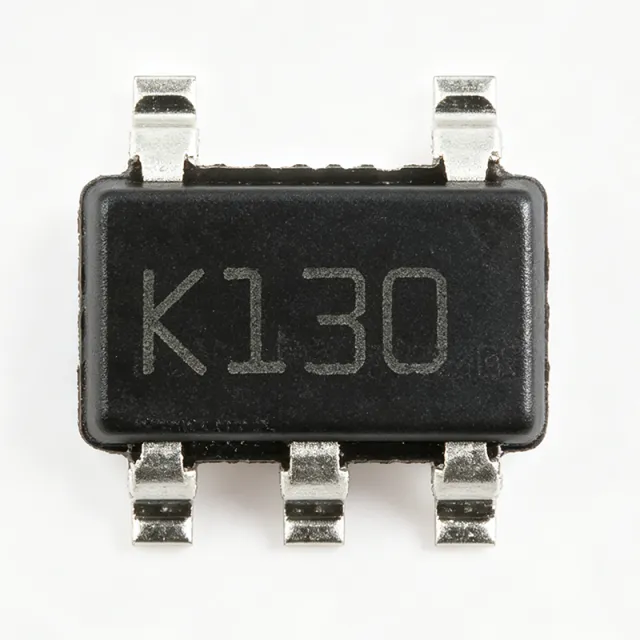
TSV991ILT - 20MHz Rail-to-Rail Op Amp | STMicroelectronics
The STMicroelectronics TSV991ILT is a single, high-speed, rail-to-rail input/output operational amplifier offering a gain-bandwidth product of 20 MHz and a slew rate of 10 V/µs. It operates from a supply voltage range of 2.5 V to 5.5 V, making it suitable for battery-powered and low-voltage applications. The device is available in the compact SOT-23-5 package, ideal for space-constrained designs. An operational amplifier (op-amp) is a high-gain voltage amplifier with differential inputs and a single-ended output. It is a fundamental building block in analog electronics, used in signal conditioning, filtering, and amplification. The TSV991ILT belongs to the family of general-purpose op-amps, which are characterized by their versatility and ease of use. In the hierarchy of analog components, op-amps are part of the broader category of linear integrated circuits, which also includes comparators and voltage regulators. Key features of the TSV991ILT include rail-to-rail input and output stages, which maximize the dynamic range in low-voltage applications. The device also features a low input offset voltage of 1.5 mV (max) and a low input bias current of 1 pA (typ), ensuring high accuracy in precision circuits. The 20 MHz bandwidth and 10 V/µs slew rate enable the amplifier to handle high-frequency signals, making it suitable for video and communication applications. The TSV991ILT is built on STMicroelectronics' advanced BiCMOS process, which combines the benefits of bipolar and CMOS technologies. This process achieves a good balance between speed, power consumption, and noise performance. The amplifier's quiescent current is typically 1.1 mA, providing a favorable trade-off between speed and power efficiency for battery-operated devices. Typical applications include active filters, signal conditioning, portable instrumentation, and audio processing. The rail-to-rail output capability allows the amplifier to drive ADC inputs directly, maximizing the usable input range. In sensor interfaces, the low input bias current minimizes errors when interfacing with high-impedance sensors. When designing with the TSV991ILT, ensure proper power supply decoupling with a 0.1 µF ceramic capacitor placed close to the VCC pin. The input common-mode voltage range extends beyond the supply rails, but care should be taken to avoid exceeding the absolute maximum ratings. The output can swing within 50 mV of the rails, which is beneficial for single-supply operation. This page synthesizes distributor pricing, drop-in alternatives, and practical design notes not found in the STMicroelectronics datasheet, providing a comprehensive resource for engineers evaluating the TSV991ILT.

TSX9292IST - 16MHz RR 16V CMOS Op-Amp, Dual | STMicroelectronics
The STMicroelectronics TSX9292IST is a dual operational amplifier featuring 16 MHz gain-bandwidth product, 27 V/µs slew rate, and 0.0003 % THD+N, housed in an 8-pin MiniSO (Mini Small Outline) package. It operates from a single 4 V to 16 V supply and provides rail-to-rail input and output swing, making it suitable for low-voltage, single-supply, and high-fidelity signal-chain designs. The two on-chip amplifiers are decompensated and stable for gains greater than +2 (or inverting gains less than -1), and each channel draws a typical 2.8 mA quiescent current. A CMOS operational amplifier (op-amp) is a high-gain DC-coupled differential amplifier built on a CMOS process. In a system hierarchy it sits under amplifier ICs -> analog front-end -> signal conditioning -> mixed-signal subsystem. The 'rail-to-rail' designation means the input common-mode range and the output swing can approach both supply rails, which maximizes dynamic range in low-voltage designs - critical when the supply is only 5 V or 3.3 V and every millivolt of headroom counts. Key features include 16 MHz GBP, 27 V/µs slew rate, 0.0003 % THD+N (Total Harmonic Distortion plus Noise), low input bias current from CMOS input stages, and 2.8 mA per-channel quiescent current. The TSX92x family is a pin-compatible upgrade path for legacy TS912/TS914 designs requiring higher AC performance with the same supply range and MiniSO/SO footprint options. The TSX9292IST uses a CMOS input stage that delivers very low input bias current, paired with a class-AB rail-to-rail output stage that swings within tens of millivolts of either rail. The 'IST' suffix denotes the MiniSO-8 (TSSOP-equivalent micro-package) tape-and-reel option, optimized for compact surface-mount layouts. Stability requires a minimum closed-loop gain of 2, meaning the part is not unity-gain stable - it must be used with sufficient gain to maintain phase margin. Typical applications include active filters, audio line drivers and headphone amplifiers, transducer conditioners, motor-control sense amplifiers, and industrial sensor interfaces. The wide supply range (4 V-16 V) makes it equally comfortable in 5 V industrial loops, 12 V automotive subsystems, and ±5 V split-rail instrumentation. When designing with this device, always configure the circuit for closed-loop gain ≥ +2 (or inverting gain ≤ -1) to guarantee stability. Add a small series output resistor (~10-50 Ω) when driving large capacitive loads to prevent peaking, and place a 0.1 µF decoupling capacitor close to each supply pin. Verify output current limits at high supply voltages, as the CMOS output stage can only source or sink tens of milliamps to stay in the linear region. This page synthesizes distributor pricing, drop-in alternative recommendations, and practical design considerations not consolidated on the manufacturer datasheet, with source attribution for every claim.