Amplifier ICs
Products (230)

ADA4807-2ARMZ - 180MHz Rail-to-Rail Op Amp | Analog Devices
The ADA4807-2ARMZ from Analog Devices is a dual-channel, low-power, low-noise, rail-to-rail voltage feedback operational amplifier. It delivers a gain bandwidth product of 180 MHz while consuming only 1 mA of supply current per amplifier, making it ideal for battery-powered and high-density applications. The device operates from a single 2.7 V to 5 V supply or dual ±1.35 V to ±2.5 V supplies, and it features rail-to-rail input and output stages that maximize dynamic range in low-voltage systems. An operational amplifier (op amp) is a high-gain voltage amplifier with differential inputs and a single-ended output, used to condition analog signals in applications such as filtering, amplification, and buffering. The ADA4807-2 is a voltage feedback amplifier, a common topology that offers stable operation with resistive feedback and is well-suited for high-speed signal processing. As a rail-to-rail input/output amplifier, it can handle input voltages that extend to both supply rails and swing its output close to the rails, which is critical in single-supply systems where headroom is limited. Key features of the ADA4807-2ARMZ include an ultra-low input voltage noise density of 3.1 nV/√Hz and current noise density of 0.7 pA/√Hz, which are among the lowest for high-speed rail-to-rail amplifiers. The device also provides a high slew rate of 225 V/µs, enabling fast signal transitions, and a wide -3 dB bandwidth of 180 MHz for small-signal applications. The amplifier is stable for gains of 1 or greater, and it includes a disable feature that reduces quiescent current to 0.3 µA when the output is placed in a high-impedance state, making it suitable for power-sensitive designs. Technically, the ADA4807-2 uses a complementary bipolar process that achieves low distortion and high linearity. The input stage employs a rail-to-rail architecture with a common-mode range that includes both rails, while the output stage uses a class-AB configuration to minimize crossover distortion. The device is specified for operation over the extended industrial temperature range of -40°C to +125°C, and it is available in the compact 8-lead MSOP package (ARMZ suffix), which is ideal for space-constrained PCBs. Typical applications include portable instrumentation, active filters, analog-to-digital converter (ADC) drivers, and buffering in data acquisition systems. The low noise and high bandwidth make it particularly well-suited for driving high-resolution ADCs, such as the AD7980 or AD4000 series, where signal integrity is paramount. In portable devices, the low quiescent current extends battery life, while the rail-to-rail output ensures maximum signal swing. When designing with the ADA4807-2ARMZ, ensure proper power supply decoupling with 0.1 µF ceramic capacitors placed close to the V+ and V- pins. The disable pin (PD) can be used for power sequencing; applying a voltage 3.4 V below the positive supply enables the device, while pulling it high disables the output. For optimal noise performance, use low-value resistors in the feedback network to minimize thermal noise contribution.
ADA4807-2ARMZ-RL7 - 180MHz Rail-to-Rail Op Amp | Analog Devices
The ADA4807-2ARMZ-RL7 is a dual, low power, low noise, rail-to-rail input/output voltage feedback amplifier from Analog Devices. It operates from a single 2.7V to 11V supply or dual ±1.35V to ±5.5V supplies, delivering 180 MHz bandwidth and a slew rate of 225 V/µs while consuming only 1 mA of quiescent current per amplifier. The device is housed in an 8-lead MSOP package, making it ideal for space-constrained, battery-powered applications. An operational amplifier (op amp) is a high-gain voltage amplifier with differential inputs and a single-ended output, used to condition signals in analog circuits. The ADA4807-2 is a voltage feedback amplifier, a type of op amp where the output voltage is proportional to the differential input voltage, offering high bandwidth and low distortion. It belongs to the family of rail-to-rail amplifiers, which can swing its output close to the supply rails, maximizing dynamic range in low-voltage systems. This device is part of the broader category of linear amplifiers, which are fundamental building blocks in signal processing chains. Key features include an ultra-low input voltage noise of 3.1 nV/√Hz and current noise of 0.7 pA/√Hz, making it one of the lowest-noise high-speed rail-to-rail amplifiers available. The rail-to-rail input and output capability allows full-scale signal swing, while the disable pin (active low) reduces quiescent current to a high-impedance state for power saving. The amplifier also features a wide supply range, making it versatile for both single and dual supply operation. Technically, the ADA4807-2 uses a bipolar process and a complementary input stage to achieve rail-to-rail operation. The device is designed for high-speed signal conditioning, with a gain bandwidth product of 180 MHz and a slew rate of 225 V/µs, enabling it to handle fast transients. The low noise and high speed make it suitable for driving high-resolution ADCs, active filters, and video applications. The output can drive capacitive loads up to 100 pF without oscillation, and the device is specified over the extended industrial temperature range of -40°C to +125°C. Typical applications include high-resolution data acquisition systems, battery-powered instrumentation, active filters, and ADC drivers. In data acquisition, the low noise and high bandwidth ensure accurate signal capture, while in battery-powered devices, the low quiescent current extends battery life. The rail-to-rail output maximizes the dynamic range of the ADC input, improving overall system performance. When designing with this device, ensure proper power supply decoupling with 0.1 µF capacitors close to the supply pins. The disable pin can be used for power sequencing, but must be driven to a logic low to enable the amplifier. For optimal noise performance, use low-value resistors in the feedback network to minimize thermal noise.

ADA4817-1ARDZ - 1GHz FastFET Op Amp | Analog Devices
The ADA4817-1ARDZ is a high-speed, unity-gain stable, voltage feedback operational amplifier with FET inputs, manufactured by Analog Devices. It features a -3 dB bandwidth of 1050 MHz, a slew rate of 870 V/µs, and a low input bias current of 2 pA. The device is offered in an 8-lead SOIC-EP package, making it suitable for high-speed signal processing applications. An operational amplifier (op amp) is a high-gain voltage amplifier with differential inputs and a single-ended output. It is a fundamental building block in analog electronics, used in signal conditioning, filtering, and amplification. The ADA4817-1ARDZ belongs to the FastFET amplifier family, which combines the high input impedance of FET inputs with the high speed of bipolar amplifiers, enabling it to buffer high-impedance sources without loading them. Key features of the ADA4817-1ARDZ include a low input bias current of 2 pA, low input capacitance, and a high slew rate of 870 V/µs. The device also offers a 0.1% settling time of 9 ns, making it ideal for fast-settling applications such as data acquisition systems and ADC drivers. The unity-gain stability ensures reliable operation in buffer configurations without external compensation. The ADA4817-1ARDZ is built on Analog Devices' proprietary eXtra fast complementary bipolar (XFCB) process, which enables its high bandwidth and low noise performance. The amplifier's low input bias current and low input capacitance make it suitable for photodiode amplifiers and other high-impedance sensor interfaces. The device operates over a wide supply voltage range, providing design flexibility. Typical applications include high-speed data acquisition, medical instrumentation, and high-speed signal processing. The amplifier's high bandwidth and fast settling time make it suitable for driving high-speed ADCs, while its low input bias current is ideal for transimpedance amplifiers in optical receivers. When designing with the ADA4817-1ARDZ, it is important to consider the thermal performance of the SOIC-EP package. The exposed pad should be soldered to a large copper area to ensure adequate heat dissipation. Additionally, proper decoupling of the power supply pins is essential to maintain high-frequency performance.
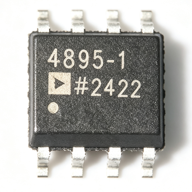
ADA4895-1ARZ - Low Noise, G≥10 Stable Op Amp | Analog Devices
The ADA4895-1ARZ is a single, high speed voltage feedback operational amplifier from Analog Devices, designed for gain ≥ 10 stability with low input noise and rail-to-rail output. It operates over a supply range of 3 V to 10 V (or ±1.5 V to ±5 V) and delivers a quiescent current of 3 mA per amplifier. The device is available in an 8-lead SOIC package and operates over the extended industrial temperature range of −40°C to +125°C. An operational amplifier (op amp) is a high-gain voltage amplifier with differential inputs and a single-ended output, used in signal conditioning, filtering, and amplification circuits. The ADA4895-1 belongs to the class of high speed voltage feedback amplifiers, which are characterized by their wide bandwidth and fast slew rate, making them suitable for applications requiring high-frequency signal processing. Within the amplifier hierarchy, it sits between general-purpose op amps and specialized RF amplifiers, offering a balance of noise performance and speed. Key features of the ADA4895-1ARZ include a 1/f noise of 2 nV/√Hz at 10 Hz, a spurious-free dynamic range (SFDR) of −72 dBc at 2 MHz, and a gain-bandwidth product of 235 MHz. The rail-to-rail output stage allows maximum output swing, and the low quiescent current of 3 mA makes it power-efficient for battery-powered designs. The device is stable for gains of 10 or greater, which simplifies compensation in non-inverting and inverting configurations. Technically, the ADA4895-1 uses a voltage feedback architecture with a complementary bipolar process, achieving low input voltage noise and high linearity. The amplifier's input stage is optimized for low noise, while the output stage provides rail-to-rail swing with low distortion. The device also features a disable pin (on the SOT-23 version) for power saving, though the SOIC version does not include this feature. Typical applications include ultrasound imaging, low noise preamplifiers, and active filters. In ultrasound systems, the low noise and high bandwidth enable accurate signal detection. In preamplifier circuits, the 2 nV/√Hz noise floor preserves weak signals. The rail-to-rail output is beneficial in single-supply applications where output swing is critical. When designing with the ADA4895-1ARZ, ensure that the gain is set to at least 10 to maintain stability. Use proper decoupling capacitors on the power supply pins, and consider the thermal performance of the SOIC package in high-power applications. The device is RoHS compliant and lead-free.
ADA4895-1ARZ-RL7 - 1nV/√Hz, G≥10 Stable Op Amp | Analog Devices
The ADA4895-1ARZ-RL7 is a single, high speed voltage feedback operational amplifier from Analog Devices, designed for gain-of-10 or greater stability. It features ultra-low input voltage noise of 1 nV/√Hz (typical) and a 1/f noise corner of 2 nV/√Hz at 10 Hz, making it an excellent choice for low-noise preamplifier and ultrasound applications. The amplifier operates over a wide supply range of 3 V to 10 V, with rail-to-rail output swing and a quiescent current of only 3 mA per amplifier, balancing high performance with power efficiency. An operational amplifier (op amp) is a high-gain voltage amplifier with differential inputs and a single-ended output, used in signal conditioning, filtering, and mathematical operations. The ADA4895-1 belongs to the class of high-speed voltage feedback amplifiers, which are optimized for wide bandwidth and fast slew rate, making them suitable for applications requiring large dynamic range and precision. Within the hierarchy of analog ICs, it sits under linear amplifiers, which are fundamental building blocks in electronic systems. Key features include a small signal bandwidth of 236 MHz at a gain of +10, a slew rate of 943 V/μs, and a settling time of 22 ns to 0.1%. The spurious-free dynamic range (SFDR) is -72 dBc at 2 MHz, ensuring low distortion in high-frequency signal paths. The device is available in an 8-lead SOIC package (ARZ suffix), with tape and reel packaging (RL7) for automated assembly. The ADA4895-1 utilizes a voltage feedback architecture with complementary bipolar transistors, achieving low noise and high speed simultaneously. The rail-to-rail output stage maximizes dynamic range, while the wide supply voltage range supports both 5 V and 10 V systems. The amplifier is stable for gains of 10 or greater, which simplifies compensation in non-inverting and inverting configurations. Typical applications include ultrasound imaging front-ends, low-noise preamplifiers for sensors, and high-speed signal conditioning in test and measurement equipment. Its low noise and high bandwidth make it ideal for amplifying small signals from photodiodes, microphones, and other transducers. When designing with this amplifier, ensure that the gain is set to at least 10 to maintain stability. Use proper power supply decoupling with 0.1 μF ceramic capacitors close to the supply pins, and consider the thermal performance of the SOIC package in high-power applications.
ADA4895-2ARZ - Dual 1nV/√Hz High Speed Op Amp | Analog Devices
The ADA4895-2ARZ is a dual, high speed voltage feedback amplifier from Analog Devices, designed for gain ≥10 stable operation with exceptional low noise performance. It features a 1/f noise of 2 nV/√Hz at 10 Hz, a large signal bandwidth of 146 MHz at gain +10, and a slew rate of 943 V/μs, settling to 0.1% in 22 ns. The amplifier operates over a wide supply voltage range of 3 V to 10 V, making it ideal for high dynamic range, precision, and high speed systems. The ADA4895-2 is available in a 10-lead MSOP package (ARZ suffix), which is compact and suitable for space-constrained designs. A high speed operational amplifier (op amp) is a voltage amplifier with a gain-bandwidth product typically exceeding 10 MHz, designed to amplify signals with fast slew rates and wide bandwidths. It is a fundamental building block in analog signal processing, used in applications such as active filters, buffers, and instrumentation. The ADA4895-2 belongs to the category of voltage feedback amplifiers, which offer high input impedance and ease of use in feedback configurations. Within the hierarchy of amplifiers, it sits as a high speed op amp, a subset of operational amplifiers, which are essential components in analog and mixed-signal systems. Key features of the ADA4895-2 include a low quiescent current of 3 mA per amplifier, rail-to-rail output, and a spurious-free dynamic range (SFDR) of -72 dBc at 2 MHz. The low input noise and high SFDR make it suitable for ultrasound, low noise preamplifiers, and other sensitive applications. The amplifier also features a wide supply range, allowing flexibility in system design. The rail-to-rail output enables maximum output swing, which is critical for single-supply operation and maximizing dynamic range. Technically, the ADA4895-2 uses a voltage feedback architecture with a complementary input stage, providing low offset voltage and high common-mode rejection. The device is fabricated using a high-speed complementary bipolar process, ensuring excellent AC performance. The amplifier is stable at gains of 10 or higher, which is specified for applications requiring high closed-loop gain. The 146 MHz bandwidth at gain +10 and 943 V/μs slew rate enable fast signal processing, while the 22 ns settling time to 0.1% ensures accurate response in pulsed applications. Typical applications include ultrasound imaging systems, low noise preamplifiers, and high speed data acquisition. In ultrasound, the low noise and high bandwidth allow for precise signal amplification from transducers. In preamplifiers, the low 1/f noise is critical for maintaining signal integrity at low frequencies. The wide supply range and rail-to-rail output make it suitable for battery-powered and single-supply systems. When designing with the ADA4895-2, ensure proper power supply decoupling with 0.1 μF and 10 μF capacitors close to the supply pins. The gain-setting resistors should be placed close to the inverting input to minimize parasitic capacitance. For optimal noise performance, use low-value resistors and keep the feedback network impedance low.
ADA4895-2ARZ-RL7 - Dual 1nV/√Hz G≥10 Stable Amp | Analog Devices
The ADA4895-2ARZ-RL7 is a dual, high speed voltage feedback amplifier from Analog Devices, designed for gain-of-10 or greater stability. It features low input noise of 1 nV/√Hz, rail-to-rail output, and a quiescent current of only 3 mA per amplifier. The device operates from a wide supply voltage range of 3 V to 10 V, making it suitable for systems requiring large dynamic range, high gain, precision, and high speed. The ADA4895-2 is available in a 10-lead MSOP package, offering a compact solution for space-constrained applications. A voltage feedback amplifier is a type of operational amplifier where the output voltage is fed back to the inverting input to control gain. The ADA4895-2 is specifically optimized for high-speed signal conditioning, providing a small signal bandwidth of 236 MHz at a gain of +10 and a slew rate of 943 V/μs. It settles to 0.1% in 22 ns, making it ideal for applications requiring fast and accurate signal processing. The rail-to-rail output stage allows maximum output swing, which is critical for driving ADCs and other mixed-signal devices. Key features of the ADA4895-2 include a 1/f noise of 2 nV/√Hz at 10 Hz, a spurious-free dynamic range of -72 dBc at 2 MHz, and a low input bias current of 11 µA. The amplifier is gain-of-10 stable, ensuring stability in high-gain configurations without external compensation. The low noise and high bandwidth make it an excellent choice for ultrasound, low noise preamplifiers, and drivers of high-performance ADCs. The ADA4895-2 utilizes a complementary bipolar process, achieving a balance between speed, noise, and power consumption. The dual configuration provides two independent amplifiers in a single package, saving board space and reducing component count. The wide supply range and rail-to-rail output enhance design flexibility, allowing the amplifier to interface with various ADC and DAC voltage levels. Typical applications include ultrasound imaging, low noise preamplifiers, ADC drivers, and active filters. The amplifier's high slew rate and fast settling time ensure accurate reproduction of high-frequency signals, while the low noise preserves signal integrity in sensitive measurement systems. When designing with the ADA4895-2, ensure proper power supply decoupling with 0.1 µF capacitors close to the supply pins. The gain-setting resistors should be placed near the amplifier to minimize parasitic capacitance and maintain stability. The thermal resistance of the MSOP package should be considered for high-power applications, although the low quiescent current minimizes self-heating.
ADA4896-2ARMZ - 1nV/√Hz Low Noise Dual Op Amp | Analog Devices
The ADA4896-2ARMZ is a dual, high-speed, voltage feedback operational amplifier from Analog Devices, offering an exceptional combination of low noise, low power, and rail-to-rail output. Housed in a compact 8-lead MSOP package, this amplifier is unity-gain stable and operates from a single 3V to 10V supply or dual ±1.5V to ±5V supplies. With a quiescent current of only 3 mA per amplifier, it delivers a bandwidth of 230 MHz and a slew rate of 120 V/µs, making it ideal for power-sensitive, high-performance signal conditioning. An operational amplifier (op amp) is a high-gain voltage amplifier with differential inputs and a single-ended output, used to perform mathematical operations like amplification, filtering, and signal conditioning. The ADA4896-2 is a voltage feedback op amp, a type that offers high input impedance and ease of use in inverting and non-inverting configurations. It belongs to the family of high-speed amplifiers, which are optimized for wide bandwidth and fast settling, essential in applications like ADC drivers, video processing, and active filters. As a rail-to-rail output amplifier, it can swing its output close to the supply rails, maximizing dynamic range in low-voltage systems. Key features of the ADA4896-2ARMZ include an ultra-low voltage noise density of 1 nV/√Hz at 100 kHz and 2.4 nV/√Hz at 10 Hz (1/f noise), a spurious-free dynamic range (SFDR) of -80 dBc at 2 MHz, and a low input bias current of 1.5 µA. The amplifier also provides a high open-loop gain of 100 dB and a common-mode rejection ratio (CMRR) of 100 dB, ensuring accurate signal processing. Its rail-to-rail output stage can drive loads as low as 50 Ω, and it is fully specified over the industrial temperature range of -40°C to +125°C. Technically, the ADA4896-2 uses a complementary bipolar process that achieves low noise without compromising speed or power. The amplifier's architecture includes a precision input stage that minimizes offset voltage (typically 0.5 mV) and drift, while the output stage provides high current drive capability. The device is designed for stable operation with capacitive loads up to 100 pF, and its internal compensation ensures unity-gain stability. The MSOP-8 package offers excellent thermal performance with a junction-to-ambient thermal resistance of 190°C/W, allowing operation in space-constrained designs. Typical applications include low-noise ADC drivers, high-speed active filters, photodiode amplification, and medical instrumentation. In ADC driver circuits, the ADA4896-2's low noise and high SFDR preserve signal integrity, while its rail-to-rail output maximizes the ADC's input range. For photodiode transimpedance amplifiers, the low input bias current and low noise enable precise detection of weak optical signals. In medical devices like ECG and EEG monitors, the amplifier's low noise and low power consumption are critical for battery-operated, high-resolution signal acquisition. When designing with the ADA4896-2ARMZ, ensure proper power supply decoupling with 0.1 µF ceramic capacitors placed close to the supply pins. The input common-mode voltage range extends to the negative rail, but for best performance, keep inputs within the specified range. The output can swing to within 50 mV of the rails, but for driving heavy loads, consider the output current capability. For optimal noise performance, use low-value resistors in the feedback network, as resistor noise can dominate.
ADA4896-2ARMZ-RL7 - Dual Low Noise RRO Op Amp | Analog Devices
The ADA4896-2ARMZ-RL7 is a dual, unity-gain stable, low noise, rail-to-rail output, high speed voltage feedback amplifier from Analog Devices. It operates on a supply voltage range of 3 V to 10 V (or ±1.5 V to ±5 V) and features a quiescent current of 3 mA per amplifier. The device is available in an 8-lead MSOP package, making it suitable for space-constrained applications. What is a voltage feedback amplifier? A voltage feedback amplifier is a type of operational amplifier where the output voltage is fed back to the inverting input through a feedback network. It is characterized by its high input impedance, low output impedance, and high open-loop gain. Voltage feedback amplifiers are widely used in signal conditioning, filtering, and buffering applications due to their ease of use and stability. They form a subset of operational amplifiers, which are fundamental building blocks in analog signal processing. Key features of the ADA4896-2 include a low 1/f noise of 2.4 nV/√Hz at 10 Hz, a spurious-free dynamic range (SFDR) of -80 dBc at 2 MHz, and a unity-gain bandwidth of 230 MHz. The rail-to-rail output stage allows maximum output swing, and the low quiescent current makes it ideal for battery-powered systems. The amplifier also features a wide supply voltage range and is specified for operation over the industrial temperature range of -40°C to +125°C. The ADA4896-2 uses a complementary bipolar process technology, providing excellent DC precision and AC performance. The device is designed to drive high-speed ADCs and other capacitive loads, with a slew rate of 120 V/µs. Its low distortion and low noise make it suitable for high-performance signal chains. Typical applications include ADC drivers, active filters, instrumentation, and portable audio equipment. The low noise and high bandwidth make it ideal for medical imaging, communications, and test and measurement systems. When designing with the ADA4896-2, ensure proper power supply decoupling with 0.1 µF capacitors close to the supply pins. The rail-to-rail output stage requires careful consideration of the load impedance to maintain stability.
ADA4897-1ARZ - 1nV/√Hz Low Noise Op Amp | Analog Devices
The ADA4897-1ARZ from Analog Devices is a unity-gain stable, low noise, rail-to-rail output, high speed voltage feedback amplifier in an 8-lead SOIC package. It operates from a 3V to 10V supply and delivers a 230 MHz bandwidth with a 120 V/µs slew rate. The device features an ultra-low wideband voltage noise of 1 nV/√Hz and a low 1/f noise of 2.4 nV/√Hz at 10 Hz, making it ideal for high-performance signal conditioning. An operational amplifier (op amp) is a high-gain voltage amplifier with differential inputs and a single-ended output. It is a fundamental building block in analog electronics, used in applications ranging from signal conditioning to active filtering. The ADA4897-1 is a voltage feedback amplifier, a type of op amp that uses a voltage-controlled voltage source topology, offering high bandwidth and low distortion. It belongs to the family of high-speed amplifiers, which are optimized for fast settling and wide bandwidth, and is part of the broader category of linear integrated circuits. Key features include a low input offset voltage of 0.5 mV (typical), a quiescent current of only 3 mA per amplifier, and a spurious-free dynamic range (SFDR) of -80 dBc at 2 MHz. The rail-to-rail output stage allows maximum output swing, and the device is unity-gain stable, simplifying design in buffer and follower configurations. The ADA4897-1 also offers low distortion of -115 dBc at 100 kHz with a 2 V p-p output, ensuring high signal fidelity. Technically, the ADA4897-1 uses a complementary bipolar process that achieves its low noise and high speed. The amplifier's input stage is optimized for low voltage noise, while the output stage provides rail-to-rail swing with low output impedance. The device is specified over the industrial temperature range of -40°C to +125°C, and it is available in an 8-lead SOIC package (ARZ suffix), which is suitable for space-constrained designs. Typical applications include low noise instrumentation, active filters, ADC drivers, and high-speed signal conditioning in test and measurement equipment. The low noise and high bandwidth make it particularly suited for medical imaging, communications, and industrial process control. In these applications, the ADA4897-1 ensures accurate signal reproduction with minimal added noise. When designing with the ADA4897-1, pay attention to power supply decoupling: place a 0.1 µF ceramic capacitor close to each supply pin and a 10 µF tantalum capacitor at the supply rails. Also, consider the thermal performance, as the SOIC package has a limited power dissipation capability; ensure the junction temperature stays below 150°C.
ADA4897-1ARZ-RL7 - 1nV/√Hz Low Noise Op Amp | Analog Devices
The ADA4897-1ARZ-RL7 is a unity-gain stable, low noise, rail-to-rail output, high speed voltage feedback amplifier from Analog Devices. It operates from a 3V to 10V supply and delivers a gain bandwidth product of 230 MHz with a slew rate of 120 V/µs. The device is available in an 8-pin SOIC package and is designed for applications requiring low noise and low power consumption. An operational amplifier (op amp) is a high-gain voltage amplifier with differential inputs and a single-ended output. It is a fundamental building block in analog electronics, used in signal conditioning, filtering, and amplification. The ADA4897-1 is a voltage feedback amplifier, which offers high bandwidth and low distortion, making it suitable for high-speed signal processing. Key features include ultra-low wideband noise of 1 nV/√Hz, low 1/f noise of 2.4 nV/√Hz at 10 Hz, and low distortion of -115 dBc at 100 kHz. The quiescent current is only 3 mA per amplifier, making it power-efficient. The rail-to-rail output stage allows maximum output swing, and the device is unity-gain stable, simplifying design. The ADA4897-1 uses a complementary bipolar process, achieving excellent noise performance and high speed. The input offset voltage is low, and the device has a high open-loop gain, ensuring accurate signal amplification. The amplifier is designed to drive capacitive loads and provides a spurious-free dynamic range of -80 dBc at 2 MHz. Typical applications include ultrasound, low noise PLLs, and high-speed instrumentation. The low noise and high bandwidth make it ideal for medical imaging, communications, and test equipment. The rail-to-rail output is beneficial in single-supply systems, and the low power consumption extends battery life in portable devices. When designing with this amplifier, ensure proper power supply decoupling with 0.1 µF capacitors close to the supply pins. The input common-mode range extends to the negative rail, but for best performance, keep inputs within the specified range. The output can swing close to the rails, but avoid heavy loads that may reduce output swing.
ADA4897-2ARMZ - Dual Low Noise RRO Op Amp | Analog Devices
The ADA4897-2ARMZ is a dual, unity-gain stable, low noise, rail-to-rail output, high speed voltage feedback amplifier from Analog Devices. It operates from a 3 V to 10 V supply and features a quiescent current of 3 mA per amplifier. The device is available in a 10-lead MSOP package, making it suitable for space-constrained applications. An operational amplifier (op amp) is a high-gain voltage amplifier with differential inputs and a single-ended output. It is a fundamental building block in analog signal processing, used in applications ranging from signal conditioning to active filtering. The ADA4897-2 belongs to the class of high-speed, low-noise amplifiers, which are essential in precision instrumentation and communication systems where signal integrity is critical. Key features of the ADA4897-2 include a low input voltage noise of 1 nV/√Hz, a 1/f noise corner of 2.4 nV/√Hz at 10 Hz, and a spurious-free dynamic range (SFDR) of 80 dBc at 2 MHz. The amplifier also provides a bandwidth of 230 MHz and a slew rate of 120 V/µs, enabling fast signal processing. The rail-to-rail output stage maximizes dynamic range, making it ideal for single-supply applications. The ADA4897-2 uses a voltage feedback architecture with complementary bipolar transistors, achieving low distortion and high linearity. The device is fully specified over the industrial temperature range of -40°C to +125°C. Its low power consumption and high speed make it a versatile choice for battery-powered and high-density systems. Typical applications include ultrasound equipment, low noise PLL filters, high performance ADC drivers, and high speed signal conditioning. The amplifier's low noise and high bandwidth ensure accurate signal reproduction in these demanding environments. When designing with the ADA4897-2, proper power supply decoupling is essential to maintain stability and minimize noise. Use 0.1 µF ceramic capacitors close to the supply pins and a 10 µF tantalum capacitor for bulk decoupling. The output can drive capacitive loads up to 100 pF without oscillation, but for larger loads, an isolation resistor may be required.
ADA4897-2ARMZ-RL7 - Dual 1nV/√Hz Low Noise Op Amp | Analog Devices
The ADA4897-2ARMZ-RL7 is a dual, unity-gain stable, low noise, rail-to-rail output, high speed voltage feedback amplifier from Analog Devices. It operates over a supply range of 3 V to 10 V and features a quiescent current of 3 mA per amplifier. The device is offered in a 10-lead MSOP package, making it suitable for space-constrained applications. An operational amplifier (op amp) is a high-gain voltage amplifier with differential inputs and a single-ended output. It is a fundamental building block in analog signal processing, used in applications such as filtering, amplification, and signal conditioning. The ADA4897-2 belongs to the class of high-speed, low-noise op amps, which are essential in precision instrumentation and communication systems. Key features include a voltage noise density of 1 nV/√Hz at 100 kHz, 1/f noise of 2.4 nV/√Hz at 10 Hz, and a spurious-free dynamic range (SFDR) of -80 dBc at 2 MHz. The amplifier provides a slew rate of 120 V/µs and a gain-bandwidth product of 230 MHz. It also features rail-to-rail output swing, enabling maximum dynamic range in low-voltage applications. The ADA4897-2 uses a complementary bipolar process, achieving low distortion and high linearity. The device is fully specified over the extended industrial temperature range of -40°C to +125°C. Its low noise and high speed make it ideal for driving high-resolution ADCs, ultrasound front-ends, and low-noise signal chains. Typical applications include ultrasound imaging, low-noise PLL loop filters, high-speed ADC drivers, and active filters. The dual configuration allows compact designs for stereo audio or multi-channel data acquisition. The rail-to-rail output ensures efficient use of the supply voltage, which is critical in battery-powered systems. When designing with this amplifier, ensure proper power supply decoupling with 0.1 µF ceramic capacitors close to the supply pins. The thermal pad (if present) should be connected to a low-impedance ground plane for optimal thermal performance. The input common-mode range extends to the negative rail, but not to the positive rail, so level shifting may be required for single-supply applications.
ADA4940-1ACPZ - Ultralow Power Differential ADC Driver | Analog Devices
The ADA4940-1ACPZ from Analog Devices is a high speed, low power differential amplifier designed to drive high performance analog-to-digital converters (ADCs). It operates from a single 3.3V to 5V supply or dual supplies, consuming only 1.25 mA quiescent current, making it ideal for battery-powered and portable applications. The device provides two closely balanced differential outputs from either differential or single-ended inputs, with a common-mode output voltage that is adjustable to match the ADC input range. A differential amplifier is an electronic amplifier that amplifies the difference between two input voltages while rejecting common-mode signals. In the context of ADC driving, it converts a single-ended signal into a balanced differential signal, improving noise immunity and increasing the dynamic range of the data acquisition system. The ADA4940-1 is fabricated on Analog Devices' advanced dielectrically isolated SiGe bipolar process, enabling high speed and low distortion. Key features include ultralow power consumption of 1.25 mA, low noise and low distortion, and a bandwidth of 34 MHz. The device supports resolutions up to 18 bits from DC to 1 MHz, making it suitable for precision data acquisition. The output common-mode voltage is adjustable via a dedicated pin, allowing direct interface to SAR and sigma-delta ADCs. The ADA4940-1 is available in a Pb-free, 3 mm × 3 mm, 16-lead LFCSP package, which is compact and suitable for space-constrained designs. Technical depth: The ADA4940-1 uses a differential architecture with internal feedback, providing excellent gain accuracy and low offset. The device features a disable pin that reduces supply current to 10 µA, enabling power cycling in portable systems. The input voltage noise is 3.9 nV/√Hz, and the distortion at 1 MHz is -100 dBc, ensuring high signal fidelity. The device operates over the industrial temperature range of -40°C to +125°C. Typical applications include driving SAR and sigma-delta ADCs in medical instrumentation, industrial process control, and portable data acquisition systems. The low power and small package make it ideal for battery-powered devices such as portable medical monitors and handheld test equipment. Design consideration: To achieve optimal performance, place a 0.1 µF decoupling capacitor close to each supply pin and use a ground plane to minimize noise. The output common-mode voltage should be set to the ADC's reference midpoint for best dynamic range.
ADA4940-1ACPZ-RL7 - Ultralow Power Differential ADC Driver | ADI
The ADA4940-1ACPZ-RL7 from Analog Devices is a low noise, low distortion fully differential amplifier designed to drive high-performance SAR and sigma-delta analog-to-digital converters (ADCs) with resolutions up to 18 bits. Operating on a mere 1.25 mA of quiescent current, it is an ideal choice for power-sensitive applications. The device is available in a compact 16-lead LFCSP-VQ (3x3 mm) package, making it suitable for space-constrained designs. A fully differential amplifier (FDA) is an amplifier that converts a single-ended input signal into a differential output, or amplifies a differential input while rejecting common-mode noise. It is a critical building block in precision data acquisition systems, providing the balanced drive required by high-resolution ADCs. The ADA4940-1 belongs to the family of differential amplifiers, which are a subset of operational amplifiers used specifically for driving ADCs and transmitting signals over long lines. Key features include ultralow power consumption of 1.25 mA quiescent current, low noise and distortion, and an adjustable output common-mode voltage. The device supports a wide supply range and provides excellent AC performance, making it suitable for applications from DC to 1 MHz. The ADA4940-1 is optimized for driving the PULSAR family of ADCs from Analog Devices, ensuring seamless integration. Technically, the ADA4940-1 employs a precision architecture that maintains low offset and high linearity. The adjustable common-mode output allows direct interface to ADC inputs, eliminating the need for external level shifting. The device also features a power-down mode to conserve energy in battery-powered systems. Its low power consumption does not compromise performance, making it a standout choice for portable instrumentation. Typical applications include driving SAR ADCs in medical imaging, industrial process control, and portable battery-powered devices. The ADA4940-1 is also used in communication systems where signal integrity is paramount. Its low power and small footprint make it ideal for multi-channel data acquisition systems. When designing with this device, ensure proper decoupling of the power supply pins and careful layout of the differential traces to minimize parasitic capacitance. The output common-mode voltage should be set to match the ADC's input range for optimal performance.
ADA4940-2ACPZ - Low Power Differential ADC Driver | Analog Devices
The Analog Devices ADA4940-2ACPZ is a dual, low power, fully differential amplifier designed for driving high-resolution SAR and sigma-delta ADCs. It operates from a single 3.3V to 7V supply or dual supplies up to ±3.5V, consuming only 1.25 mA quiescent current per amplifier. The device provides two closely balanced differential outputs from either differential or single-ended inputs, making it ideal for precision data acquisition systems. A fully differential amplifier (FDA) is an amplifier with differential inputs and differential outputs, used to convert single-ended signals to differential, buffer differential signals, and drive ADCs. It is a key building block in signal chains, sitting between the sensor/amplifier stage and the ADC, ensuring optimal signal integrity and common-mode rejection. The ADA4940-2 belongs to the family of differential amplifiers, which are a subset of operational amplifiers, which are part of the broader category of analog integrated circuits. Key features include a -3 dB bandwidth of 26 MHz, a slew rate of 45 V/µs, and a low input voltage noise of 3.9 nV/√Hz. The device achieves a spurious-free dynamic range (SFDR) of -110 dBc at 100 kHz and a THD of -110 dB at 100 kHz, ensuring high fidelity for precision applications. It also features an output common-mode voltage control pin (VOCM) for level shifting, and a power-down pin for standby operation. The ADA4940-2 is fabricated on Analog Devices' advanced dielectrically isolated SiGe bipolar process, providing excellent DC accuracy with a maximum input offset voltage of 150 µV and a typical offset drift of 0.5 µV/°C. The device is available in a Pb-free, 4 mm × 4 mm, 24-lead LFCSP package, which is compact and suitable for space-constrained designs. Typical applications include driving PULSAR ADCs, such as the AD7985 and AD7986, in medical imaging, industrial process control, and instrumentation. The low power consumption and high performance make it suitable for battery-powered portable devices and multi-channel data acquisition systems. When designing with the ADA4940-2, ensure proper supply decoupling with 0.1 µF capacitors close to the supply pins. The VOCM pin should be driven by a low-impedance source to set the output common-mode voltage, and the feedback network should be matched to maintain balance and minimize distortion.
ADA4940-2ACPZ-RL7 - Ultralow Power ADC Driver | Analog Devices
The ADA4940-2ACPZ-RL7 from Analog Devices is a dual, ultralow power, low distortion fully differential amplifier (FDA) designed to drive high-performance SAR and sigma-delta ADCs with resolutions up to 18 bits. Operating from a single 3.3V to 7V supply or dual supplies up to ±3.5V, it consumes only 1.25 mA of quiescent current per amplifier, making it ideal for battery-powered and power-sensitive applications. The device is housed in a 24-lead LFCSP (4mm x 4mm) package with an exposed pad for enhanced thermal performance. A fully differential amplifier (FDA) is an operational amplifier with differential inputs and differential outputs, providing balanced signals that reject common-mode noise and even-order harmonics. FDAs are essential in precision data acquisition systems, where they convert single-ended signals to differential for driving ADCs, improving dynamic range and reducing distortion. The ADA4940-2 belongs to the ADA4940 family, which includes the single-channel ADA4940-1 and the dual ADA4940-2, both offering the same low noise and low distortion performance. Key features include a low input voltage noise of 3.9 nV/√Hz, a spurious-free dynamic range (SFDR) of -110 dBc at 100 kHz, and a -3 dB bandwidth of 26 MHz. The output common-mode voltage is adjustable via a VOCM pin, allowing precise level shifting to match the ADC input range. The device also features a disable pin for power-down, reducing quiescent current to 10 µA, and an internal common-mode feedback loop that maintains output balance. The ADA4940-2 uses a precision bipolar process with laser-trimmed thin-film resistors, achieving low DC offset (typically 50 µV) and excellent gain accuracy. Its differential output swing is rail-to-rail, and it can drive capacitive loads up to 10 pF without oscillation. The device is fully specified over the -40°C to +125°C temperature range, ensuring reliable operation in industrial and automotive environments. Typical applications include driving SAR ADCs such as the AD7985 and AD7768, medical imaging systems, portable instrumentation, and communications receivers. The low power consumption and small footprint make it suitable for multi-channel data acquisition systems where board space and thermal budget are constrained. When designing with the ADA4940-2, ensure proper supply decoupling with 0.1 µF and 10 µF capacitors close to the VCC and VEE pins. The VOCM pin should be driven by a low-impedance source to avoid common-mode errors. For optimal distortion, keep the feedback resistor values between 200 Ω and 1 kΩ and minimize parasitic capacitance at the summing nodes.
ADA4941-1ARZ - 18-Bit Differential ADC Driver | Analog Devices
The ADA4941-1ARZ is a low power, single-ended input, differential output amplifier optimized for driving high resolution analog-to-digital converters (ADCs). Manufactured on Analog Devices' proprietary second-generation eXtra fast complementary bipolar (XFCB) process, it achieves 18-bit performance on low supply currents. The device is configured in an easy-to-use, single-ended-to-differential gain of +2 configuration, making it ideal for precision data acquisition systems. A differential ADC driver is an amplifier that converts a single-ended input signal into a differential output, which is required by many high-performance ADCs to improve noise immunity and dynamic range. The ADA4941-1 belongs to the class of differential amplifiers, which are essential building blocks in signal chains for precision measurement, medical imaging, and communications. By providing a balanced output, it enables the full-scale input range of the ADC to be utilized, enhancing the signal-to-noise ratio (SNR) and reducing even-order harmonics. Key features include ultralow distortion of 120 dBc THD at 10 kHz, low noise achieving 97 dB SNR at 100 kHz with 4 V p-p output, and extremely low power consumption on a 3 V supply. The device operates from a single supply, simplifying power design. It offers high input impedance, which minimizes loading on the preceding stage. The ADA4941-1 is available in an 8-lead SOIC package (ARZ suffix), suitable for space-constrained applications. Technically, the ADA4941-1 uses a differential architecture with an internal common-mode feedback loop that sets the output common-mode voltage to a reference level, typically mid-supply. This allows direct coupling to ADCs with a specified common-mode input range. The XFCB process provides high-speed complementary bipolar transistors with excellent matching, contributing to the low distortion and noise performance. The device is stable with capacitive loads, simplifying PCB layout. Typical applications include driving 16-bit and 18-bit PulSAR ADCs such as the AD7687, AD7690, and AD7691. It is also used in industrial process control, medical instrumentation, and communications systems where high resolution and low power are critical. The single-ended-to-differential conversion capability makes it versatile for interfacing sensors and transducers to differential ADCs. When designing with the ADA4941-1, ensure proper supply decoupling with 0.1 uF and 10 uF capacitors close to the VCC and VEE pins. The output common-mode voltage can be adjusted via the VOCM pin to match the ADC input range. For optimal performance, use precision resistors with low temperature coefficient for the gain-setting network.
ADA4941-1ARZ-RL7 - Differential ADC Driver | Analog Devices
The ADA4941-1ARZ-RL7 is a low power, single-ended input, differential output amplifier optimized for driving high resolution analog-to-digital converters (ADCs). Manufactured by Analog Devices on their proprietary second-generation eXtra fast complementary bipolar (XFCB) process, this device achieves 18-bit performance on low supply currents. It is configured in an easy-to-use, single-ended-to-differential gain of +2 configuration, making it ideal for driving 16-bit and 18-bit PulSAR ADCs such as the AD7687, AD7690, and AD7691. A differential ADC driver is an amplifier that converts a single-ended input signal into a differential output, which is required by many high-performance ADCs to improve noise immunity and dynamic range. The ADA4941-1 belongs to the category of differential amplifiers, which are a subset of operational amplifiers used in signal conditioning chains. These amplifiers are essential in precision data acquisition systems where the ADC's performance depends on the quality of the driving signal. Key features of the ADA4941-1 include ultralow distortion of 120 dBc THD at 10 kHz, low noise enabling 97 dB SNR at 100 kHz with a 4 V p-p output, and extremely low power consumption on a 3 V supply. The device operates from a single supply, simplifying power supply design. Its high input impedance minimizes loading on the source, and the differential output provides the balanced drive required by modern ADCs. Technically, the ADA4941-1 uses a single-ended to differential conversion with a fixed gain of +2, eliminating the need for external gain-setting resistors. The output common-mode voltage is set by an internal reference, ensuring proper ADC input range. The XFCB process provides high speed and low distortion while maintaining low power, making it suitable for battery-powered and portable instrumentation. Typical applications include driving 16-bit and 18-bit SAR ADCs in medical imaging, industrial process control, and precision data acquisition systems. The device is also used in communication systems where high dynamic range is required. Its low power consumption makes it ideal for portable and battery-operated equipment. When designing with the ADA4941-1, ensure that the input signal is within the common-mode input range and that the output is properly filtered to avoid aliasing. The device is available in an 8-lead SOIC package, and the RL7 suffix indicates tape and reel packaging for automated assembly.
ADA4945-1ACPZ - Low-Noise FDA ADC Driver | Analog Devices
The ADA4945-1ACPZ is a low-noise, low-distortion, fully differential amplifier (FDA) from Analog Devices, designed for driving high-performance ADCs in data acquisition and signal processing systems. It operates over a broad power supply range of 3 V to 10 V and is available in a compact 16-lead LFCSP (3x3 mm) package. The device features two selectable power modes, allowing designers to trade off power consumption against bandwidth and noise performance, making it highly flexible for a variety of applications. A fully differential amplifier (FDA) is an amplifier with differential inputs and differential outputs, typically used to convert single-ended signals to differential signals or to drive differential-input ADCs. FDAs are essential in high-speed signal chains because they provide common-mode rejection, reduce even-order harmonics, and improve signal integrity by maintaining a balanced signal path. The ADA4945-1 fits into the hierarchy of amplifiers: fully differential amplifier -> differential amplifier -> operational amplifier -> analog IC -> semiconductor. Key features of the ADA4945-1 include low DC offset and offset drift (0.1 µV/°C), excellent dynamic performance, and rail-to-rail output. The device also includes an output common-mode voltage control pin, enabling precise setting of the ADC input common-mode voltage. The two power modes (full power and low power) allow optimization for either maximum bandwidth or reduced power consumption, with a typical quiescent current of [DATA_NEEDED: quiescent current] in full power mode. Technically, the ADA4945-1 uses a high-voltage process to support 10 V operation, which is higher than many competing FDAs. This enables it to drive ADCs with larger input ranges and provides greater headroom. The device also features output limiting, which protects the ADC from overdrive conditions. The low noise and distortion characteristics make it ideal for precision measurement and communications applications. Typical applications include ADC drivers for high-speed data acquisition, medical imaging, communications receivers, and industrial instrumentation. The ADA4945-1 is particularly well-suited for driving ADCs such as the AD9680, AD9268, and AD9656, which are available on XAIPART. Its low offset drift ensures accurate DC performance over temperature, while the rail-to-rail output maximizes dynamic range. When designing with the ADA4945-1, it is important to properly set the output common-mode voltage using the VOCM pin and to select the appropriate power mode for the application. The device requires careful PCB layout to minimize parasitic capacitance and maintain signal integrity. Refer to the ADA4945-1 data sheet for detailed application circuits and layout guidelines.
ADA4945-1ACPZ-RL7 - Low Noise FDA ADC Driver | Analog Devices
The ADA4945-1ACPZ-RL7 from Analog Devices is a low-noise, low-distortion, fully differential amplifier (FDA) designed for driving high-performance ADCs. It operates over a broad power supply range of 3 V to 10 V and features two selectable power modes, allowing designers to optimize between power consumption and dynamic performance. The device is offered in a compact 16-lead LFCSP (3x3 mm) package, making it suitable for space-constrained applications. A fully differential amplifier (FDA) is an amplifier with differential inputs and differential outputs, providing balanced signals that reject common-mode noise and even-order harmonics. FDAs are essential in high-speed signal chains, particularly for driving ADCs, where they convert single-ended signals to differential, provide gain, and buffer the ADC input. The ADA4945-1 fits into the hierarchy: fully differential amplifier -> differential amplifier -> operational amplifier -> analog IC -> semiconductor. Key features include ultra-low DC offset and offset drift (0.1 µV/°C), high speed, and excellent distortion performance. The device achieves low noise and low distortion, making it ideal for data acquisition systems requiring high accuracy. The two power modes allow a trade-off between power dissipation and bandwidth, enabling efficient operation in battery-powered or high-performance systems. Technically, the ADA4945-1 uses a precision architecture with internal common-mode feedback, ensuring accurate output common-mode voltage control. It provides a wide input common-mode range and rail-to-rail output, simplifying interface with various ADC inputs. The device also includes a disable feature for power saving, and its small package minimizes board space. Typical applications include driving high-speed ADCs in communications, instrumentation, and medical imaging systems. It is also used in single-ended to differential conversion, level shifting, and as a buffer for precision references. The low offset drift ensures stable performance over temperature, critical for precision measurement. When designing with the ADA4945-1, ensure proper power supply decoupling with 0.1 µF and 10 µF capacitors close to the pins. The feedback network must be carefully matched to maintain balance and minimize distortion. The device's power mode selection should be based on the required bandwidth and power budget.
ADA4950-1YCPZ - Differential ADC Driver G=1/2/3 | ADI
The ADA4950-1YCPZ is a low power, selectable gain differential ADC driver from Analog Devices, Inc. It provides fixed gains of 1, 2, or 3 using on-chip feedback and gain resistors, eliminating the need for external resistor networks and reducing BOM area. The device is packaged in a 16-lead LFCSP-VQ (3x3 mm) and supports a single supply range of 3 V to 11 V or a dual supply range of ±1.5 V to ±5.5 V. It is designed for driving high performance analog-to-digital converters (ADCs) in both single-ended-to-differential and differential-to-differential configurations. A differential ADC driver is a specialized amplifier that converts a single-ended or differential analog signal into a balanced differential output centered at a desired common-mode voltage, which is essential for driving modern high-speed ADCs. These converters rely on differential inputs to improve common-mode noise rejection, reduce even-order harmonic distortion, and double the dynamic range compared with single-ended driver solutions. Within the signal chain hierarchy, the ADC driver sits between the anti-aliasing filter and the converter input, providing scaling, buffering, and level shifting. Key features of the ADA4950-1 include on-chip gain select pins for G=1, 2, 3, low power consumption enabled by the proprietary silicon-germanium (SiGe) complementary bipolar process, and 114 mA output current per channel. The internal feedback network maintains excellent gain accuracy without external precision resistors, and the low distortion and noise floor suit demanding data acquisition and communications applications. The SiGe complementary bipolar fabrication process provides the ADA4950-1 with a favorable speed-to-power ratio, making it possible to achieve wide bandwidths and low harmonic distortion while consuming less quiescent current than amplifiers built in older bipolar processes. The ADA4950-1 is the single-channel version; the ADA4950-2 is the dual-channel companion for multichannel systems. Typical applications include high-speed ADC input stages in instrumentation, IF sampling and baseband signal chains in software-defined radios, differential buffering for sensors, and ultrasound and radar preprocessing. The 3x3 mm LFCSP package supports compact board layouts. When designing with the ADA4950-1, connect the gain select pins according to the desired closed-loop gain and place 0.1 uF decoupling capacitors as close as possible to the supply pins. The output common-mode voltage must be set within the ADC input range to avoid clipping and preserve converter dynamic performance.
ADA4950-1YCPZ-RL7 - Selectable Gain Diff ADC Driver | Analog Devices
The ADA4950-1YCPZ-RL7 from Analog Devices is a low power, selectable gain differential ADC driver with on-chip feedback and gain resistors. It is a gain-selectable version of the ADA4932-1, offering gains of 1, 2, and 3 without external resistors. The device is housed in a 16-lead LFCSP-VQ (3x3 mm) package and is designed to drive high performance analog-to-digital converters (ADCs) in both single-ended-to-differential and differential-to-differential configurations. A differential amplifier is an electronic amplifier that amplifies the difference between two input voltages while rejecting common-mode signals. In the signal chain hierarchy, a differential ADC driver sits between the sensor or analog front-end and the ADC, converting single-ended signals to differential or buffering differential signals to provide the low impedance, high linearity drive required for high-resolution conversion. This function is critical in applications such as communications, instrumentation, and medical imaging where signal integrity directly impacts system performance. Key features of the ADA4950-1 include selectable gains of 1, 2, and 3 via a single gain pin, eliminating the need for external resistor networks and reducing component count. The device operates from a single 3.3V to 5V supply or dual supplies up to ±5V, and features a wide bandwidth suitable for driving ADCs with sample rates up to 100 MSPS. The low power consumption of 5.5 mA quiescent current makes it ideal for battery-powered and channel-dense systems. The output common-mode voltage is adjustable, allowing direct interface to ADC input ranges. Technically, the ADA4950-1 uses an internal feedback network with precision laser-trimmed resistors to achieve accurate gains and low distortion. The device provides a differential output with a common-mode reference pin (VOCM) that sets the output common-mode level, simplifying ADC interface design. The input voltage noise is 3.5 nV/√Hz, and the spurious-free dynamic range (SFDR) is excellent, ensuring high fidelity signal conversion. The LFCSP package with exposed pad offers good thermal performance and a compact footprint for space-constrained designs. Typical applications include driving high-speed ADCs in communications receivers, medical ultrasound equipment, and test and measurement instruments. The selectable gain feature allows the same board design to accommodate different input signal levels, reducing design time and BOM cost. The device is also suitable for differential signaling over twisted-pair cables in industrial and automotive systems. When designing with the ADA4950-1, ensure proper power supply decoupling with 0.1 µF and 10 µF capacitors close to the supply pins. The VOCM pin should be driven by a low-impedance source to set the output common-mode voltage accurately. The gain select pin (G1) must be tied to the appropriate logic level to achieve the desired gain, and the input pins should be AC-coupled if the source has a DC offset.
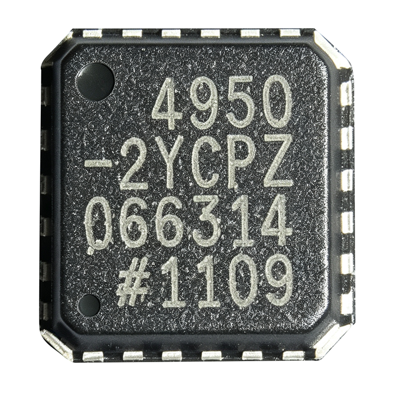
ADA4950-2YCPZ - Dual Differential ADC Driver | Analog Devices
The ADA4950-2YCPZ is a dual, gain-selectable differential amplifier from Analog Devices, designed as a high-performance ADC driver. It is a member of the ADA4950 family, which includes the ADA4950-1 (single) and ADA4950-2 (dual) versions. These amplifiers feature on-chip feedback and gain resistors, allowing fixed gains of 1, 2, and 3 without external components. The ADA4950-2 is fabricated using Analog Devices' proprietary silicon-germanium (SiGe) complementary bipolar process, which enables low distortion and low noise at low power consumption. The device operates from a single 3.3V to 11V supply or dual ±1.65V to ±5.5V supplies, and is available in a 24-lead LFCSP (4x4 mm) package. A differential amplifier is an electronic amplifier that amplifies the difference between two input voltages while rejecting common-mode signals. In the context of ADC driving, a differential amplifier converts a single-ended signal to a differential signal or buffers a differential signal, providing the necessary drive strength and level shifting to interface with high-performance analog-to-digital converters. The ADA4950-2 is specifically optimized for this role, offering low noise, low distortion, and high bandwidth to preserve signal integrity. Key features of the ADA4950-2 include a -3 dB bandwidth of 1.35 GHz (gain = 1), a slew rate of 2900 V/µs, and a low input voltage noise of 2.2 nV/√Hz. The device provides a differential output with a common-mode voltage set by an internal reference, simplifying interface to ADCs. It also features a power-down mode to conserve energy when not in use. The on-chip gain resistors eliminate the need for external resistor networks, reducing board space and component count. The ADA4950-2 is well-suited for a wide range of applications, including communications, instrumentation, and medical imaging. Its high bandwidth and low distortion make it ideal for driving high-speed ADCs in software-defined radios, radar systems, and test equipment. The low power consumption (typically 9.5 mA per amplifier) is beneficial for portable and battery-powered devices. When designing with the ADA4950-2, it is important to consider proper power supply decoupling and PCB layout to achieve optimal performance. The exposed pad on the LFCSP package should be soldered to a ground plane for thermal and electrical performance. Additionally, the input common-mode voltage range and output swing should be checked against the ADC's input requirements to ensure proper operation.