Battery Management
Products (65)

ADBMS6948 - 16-Channel Battery Monitor | Analog Devices
The ADBMS6948 is a 16-channel battery pack monitoring system from Analog Devices, designed for measuring up to 16 series-connected battery cells with exceptional accuracy. It features the industry's first parallel measurement architecture, enabling simultaneous cell voltage and pack current measurements. The device achieves a total measurement error (TME) of less than 3 mV over the full temperature range and lifetime, making it suitable for demanding automotive and energy storage applications. The ADBMS6948 operates over a measurement range of -2.5V to 5.5V, supporting various battery chemistries including NMC and LFP. It is available in a 64-lead LFCSP-SS (9x9 mm) package. A battery pack monitoring system is an integrated circuit that measures the voltage, current, and temperature of individual cells in a battery pack to ensure safe and efficient operation. It is a critical component in battery management systems (BMS), which are used in electric vehicles, energy storage systems, and backup power supplies. The ADBMS6948 belongs to the category of battery monitoring ICs, which are part of the broader power management integrated circuit (PMIC) family. These devices provide essential data for state-of-charge (SoC) and state-of-health (SoH) estimation, cell balancing, and protection against overvoltage, undervoltage, and overcurrent conditions. Key features of the ADBMS6948 include synchronous pack current and cell voltage measurements, short/over current detection with less than 2 μs response time, programmable detection time and threshold, dedicated outputs for MOSFET/contactor control, redundant measurement, algorithm, and fault pin, 10 general-purpose I/O (GPIO) channels, cell and board temperature measurements, and pack, load, and system diagnostic measurements. The device also includes an SPI interface with a maximum operating frequency of [DATA_NEEDED: SPI max frequency] MHz, enabling high-speed communication with a host microcontroller. The ADBMS6948's parallel measurement architecture is a significant advancement over traditional sequential measurement systems, as it allows simultaneous sampling of all cell voltages and pack current, improving the accuracy of power and energy calculations. This is particularly important in applications where load transients can cause voltage fluctuations, as the synchronous measurement ensures that the voltage and current readings are time-aligned. The device also features a dedicated FAULTB pin that generates an interrupt when any preprogrammed over or under thresholds on cell voltage, cell temperature, or delta measurements are violated, providing immediate fault notification to the system controller. Typical applications for the ADBMS6948 include mild hybrid electric vehicles, two-wheeler and three-wheeler electric vehicles, four-wheeler electric vehicle auxiliary batteries, backup battery systems, and energy storage systems (ESS). Its high accuracy and robust feature set make it ideal for automotive battery management, where safety and reliability are paramount. The device's ability to measure both cell voltages and pack current synchronously enables precise state-of-charge estimation, which is essential for maximizing battery life and performance. When designing with the ADBMS6948, it is important to consider the PCB layout to minimize noise and ensure accurate measurements. The device requires careful decoupling of the power supply and proper grounding to achieve the specified TME. Additionally, the SPI interface should be isolated if the battery pack is at a high potential relative to the host controller, using components such as the ADuM1441ARWZ digital isolator. The ADBMS6948 is recommended for new designs, indicating that it is a current product with ongoing support from Analog Devices.
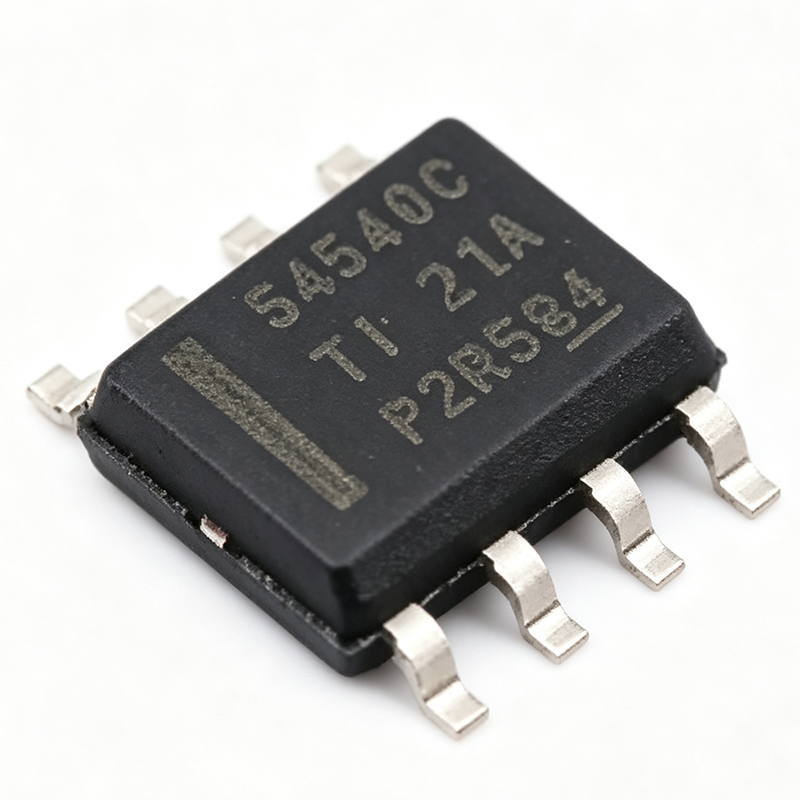
BQ24133QRGYRQ1 - 2.5A 1-3 Cell Buck Charger Q1 | TI
The Texas Instruments BQ24133QRGYR is an automotive-grade (AEC-Q100) stand-alone 1.6-MHz synchronous switched-mode Li-Ion and Li-Polymer battery charger with two integrated N-channel power MOSFETs, delivered in a 24-pin VQFN (RGY, 5.5x3.5 mm) package. It charges 1-cell, 2-cell, or 3-cell battery stacks at up to 2.5 A with a regulated 4.2 V/cell charge voltage. A switched-mode battery charger is a DC-DC converter-based power management IC that regulates charge current and battery voltage with far higher efficiency than linear chargers. Within the power-management IC hierarchy, the BQ24133 family sits between a generic buck regulator and a full battery management IC, adding charge termination, thermal regulation, and adapter-to-battery power path selection. Key features include a 1.6-MHz constant-frequency synchronous PWM controller delivering up to 92% efficiency, a 30-V input rating with adjustable input overvoltage protection, a 4.5-V to 17-V operating input range, and an automatic power path selector between the adapter and battery. High-accuracy regulation of input current, charge current, and charge voltage enables the device to safely work with limited-adapter-power systems, while dynamic power management protects overloaded sources. The device closely monitors battery pack temperature (TS pin with NTC) and permits charging only within a preset temperature window, an essential safety behavior for automotive and industrial lithium batteries. Integrated MOSFETs eliminate external discrete transistors, shrinking the solution footprint and reducing BOM count. Typical applications include automotive infotainment and telematics backup batteries, industrial handheld instruments, portable medical devices, and battery-backed servers or gateways requiring seamless adapter-to-battery transition. The power path feature keeps the system alive even with a deeply discharged battery. Design consideration: the 1.6-MHz switching frequency permits small inductors, but PCB layout of the power loop must be tight; place the inductor, input capacitor, and PGND connections per the datasheet layout guidelines to minimize EMI.

BQ24133RGYR - 2.5A 1.6MHz Sync Buck Charger | TI
The Texas Instruments BQ24133RGYR is a highly integrated stand-alone Li-Ion and Li-Polymer switched-mode battery charger with two integrated N-channel power MOSFETs. It operates as a 1.6-MHz synchronous buck charger delivering up to 2.5A charge current for 1-3 cell battery packs, housed in a 24-pin VQFN (RGY) package measuring 5.5x3.5 mm for space-constrained portable designs. A battery charger IC is a power-management device that safely controls charging current and voltage for rechargeable cells. The BQ24133 uses a synchronous buck converter topology to step down input voltage efficiently, minimizing heat compared to linear chargers. It belongs to the battery management IC hierarchy within power management semiconductors, essential for portable electronics, tools, and medical devices. Key features include high-accuracy regulation with plus/minus 1% charge voltage accuracy, a wide input range from a DC source as high as 17V including automotive car batteries, and an adjustable input overvoltage limit via the OVPSET pin with 30V rating on AVCC, ACP, and ACN pins. An integrated power path selector lets the system run from the adapter while charging the battery, and an external thermistor enables charging only within a safe temperature window. Technically, the constant-frequency synchronous PWM controller at 1.6 MHz permits small inductors and capacitors. Charge current is programmable via an external resistor, and cell count is configured for 1, 2, or 3 series cells. Thermal regulation reduces charge current when die temperature exceeds threshold, and a low-power sleep mode minimizes battery drain when input is removed. On high-voltage DC insertion, Q1 and Q2 remain off to protect the system. Typical applications include smartphones, tablets, digital cameras, power banks, solar-powered chargers, battery-powered industrial equipment, and medical devices. Design tip: ensure adequate copper pour for thermal dissipation and place input/output capacitors close to the IC; select the inductor based on the 1.6-MHz switching frequency to minimize ripple.
BQ24251RGER - 2A I2C Li-Ion Charger IC | Texas Instruments
The Texas Instruments BQ24251RGER is a 2A single-input, I2C/standalone switched-mode Li-Ion battery charger with power-path management, housed in a 24-pin VQFN (4x4 mm) package. It integrates a high-efficiency synchronous buck charger, power-path management, and USB/BC1.2 detection, enabling efficient charging from USB or AC adapters while powering the system independently of battery presence. A battery charger IC is a power management device that regulates the charging of rechargeable batteries, ensuring safe and efficient energy transfer. The BQ24251 belongs to the battery charger IC family, which falls under battery management ICs, a subset of power management integrated circuits (PMICs). These devices are essential in portable electronics, where they manage charge current, voltage, and thermal conditions to extend battery life and ensure safety. Key features include a selectable input current limit of 100 mA, 500 mA, 900 mA, 1.5 A, and 2 A, USB charging compliance, BC1.2-compatible D+/D- detection in host mode, and a separate power path that allows system startup from a deeply discharged or missing battery. The I2C interface enables dynamic control of charge parameters, while standalone mode supports autonomous operation without host intervention. The BQ24251 uses a switched-mode architecture with a high-efficiency synchronous buck converter, achieving up to 92% efficiency. It integrates power-path management, which prioritizes system load over battery charging, reducing battery cycling and enabling instant-on functionality. The device also includes safety features such as thermal regulation, overvoltage protection, and a watchdog timer. Typical applications include smartphones, tablets, portable media players, and other USB-powered devices. Its power-path management makes it ideal for applications requiring instant system operation even with a depleted battery, such as GPS units and handheld medical devices. When designing with the BQ24251, ensure proper PCB layout with adequate ground plane and input/output capacitor placement to minimize noise and optimize thermal performance. The I2C address and charge parameters should be configured according to the system requirements, and the watchdog timer must be serviced in host mode to avoid unintended shutdown.
BQ24610QRGERQ1 - 1-6 Cell Buck Battery Charger Q1 | Texas Instruments
The Texas Instruments BQ24610QRGERQ1 is an AEC-Q100 qualified, stand-alone synchronous switch-mode battery charge controller for 1- to 6-cell Li-ion and Li-polymer batteries, housed in a 24-pin VQFN (RGE, 4x4 mm) package. As part of the automotive-grade BQ2461x-Q1 family, it drives external N-channel MOSFETs in a synchronous buck topology for high-efficiency charging. A battery charge controller is a power management IC that regulates current and voltage delivered to rechargeable cells. The BQ24610 manages the full charge profile: preconditioning (trickle charge for deeply discharged cells), constant-current (CC) fast charge, constant-voltage (CV) regulation, and charge termination, with automatic recharge when the battery voltage falls below the recharge threshold. Key features include a constant-frequency current-mode PWM controller with high-accuracy charge current and voltage regulation (0.5% charge voltage accuracy), an integrated system power selector (NVDC-style power path) that allows the system to boot from the adapter even with a deeply discharged or absent battery, adapter current regulation to prevent adapter overload, and low quiescent current for efficiency. Charge status outputs and safety timers provide monitoring and fault protection including thermal shutdown and battery temperature qualification via TS pin (JEITA-style NTC monitoring). The controller architecture keeps power losses in external components, enabling charge currents of several amperes set by the external sense resistor, with programmable switching frequency for inductor and MOSFET optimization. Input voltage operating range supports common automotive and adapter rails up to 28 V. Typical applications include automotive infotainment and telematics backup batteries, portable industrial instruments, medical handheld devices, and 1-6 cell battery-powered systems requiring power-path management. For a non-automotive equivalent, the BQ24610RGER shares the same die and footprint. Design tip: size the sense resistor for the target fast-charge current (Rsense = 50 mV / Ichg typical), and follow the TI datasheet layout guidelines to place the bootstrap capacitor, gate-drive loops, and NTC network close to the IC for robust synchronous buck operation.
BQ24610RGER - Stand-Alone Sync Li-Ion Battery Charger | TI
The Texas Instruments BQ24610RGER is a highly integrated, stand-alone synchronous switch-mode battery charge controller for Li-ion, Li-polymer, and lead-acid batteries, housed in a 24-pin VQFN (4x4 mm, RGE) package with exposed thermal pad. It supports up to 6 cells in series and delivers high-accuracy charge current and voltage regulation with system power selector functionality. A battery charge controller is a power management IC that regulates charging of rechargeable batteries, managing charge current, voltage regulation, preconditioning, and termination for safety and battery longevity. The BQ24610 belongs to the switched-mode charger family within the broader power management IC hierarchy, using a constant-frequency synchronous PWM controller to achieve far higher efficiency than linear chargers, which reduces heat dissipation in space-constrained designs. Key features include a constant-frequency synchronous buck PWM controller with external MOSFETs for charge currents up to 10 A, high-accuracy regulation (0.5% charge voltage accuracy), adapter current regulation (input DPM), and charge status monitoring. Three-phase charging - preconditioning, constant current, and constant voltage - maximizes battery life. A system power selector allows the system load to run from the adapter or battery, while low quiescent current conserves battery energy during storage. Technically, the BQ24610RGER implements a proprietary voltage regulated loop with programmable termination, safety timers, thermal regulation, and fault protection. Synchronous rectification reduces conduction losses; the controller architecture keeps external FETs off-package, allowing charge current to be scaled to the application needs. Stand-alone operation requires no host microcontroller for basic charging functions, simplifying system design. Typical applications include notebook and tablet power banks, portable instruments, power tools, ePOS terminals, and medical devices requiring continuous system operation during charging (power path management). Design tip: ensure proper PCB layout with thermal vias under the exposed pad, place the charge current sense resistor near the IC to reduce noise, and set the input DPM threshold to match the adapter rating to prevent adapter overload. Pricing shown reflects estimates as of 2026-08-29.
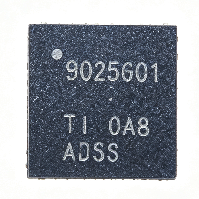
BQ25601RTWR - 3A I2C Buck Battery Charger | Texas Instruments
The Texas Instruments BQ25601RTWR is a highly integrated I2C-controlled 3A single-cell battery charger with Narrow Voltage DC (NVDC) power path management, designed for high input voltage applications. It operates from an input voltage range of 3.9V to 13.5V (14V absolute maximum) and supports a charge current up to 3A, in a 24-pin WQFN (4x4mm) RTW package over -40C to +85C. A battery charger IC is a power management integrated circuit that regulates the charging of rechargeable batteries, ensuring safe and efficient charging while protecting the battery from overvoltage, overcurrent, and overtemperature conditions. Within the power management IC hierarchy, the BQ25601 integrates a synchronous buck converter, NVDC power path management, and an I2C interface, enabling dynamic power management between the input source, system load, and battery. This allows the system to boot and operate even when the battery is deeply discharged or absent. Key features include a 3A fast-charge current, adjustable charge voltage from 3.856V to 4.624V, high input voltage support up to 13.5V, and an integrated bootstrap diode for the high-side gate drive that simplifies system design and reduces BOM count. The I2C serial interface provides programmable charge current, charge voltage, and input current limits, and supports On-The-Go (OTG) boost operation from the battery to power attached USB peripherals. The BQ25601 uses a synchronous buck topology with a high-efficiency power stage, achieving approximately 92% efficiency at typical operating conditions. Input voltage and current regulation (DPM) deliver maximum charging power from USB adapters and other sources, while protections include input overvoltage, battery overvoltage, and thermal shutdown. Typical applications include smartphones, tablets, portable speakers, power banks, and industrial or medical handheld devices requiring reliable high-current single-cell charging with power path management. When designing with the BQ25601, ensure a proper PCB layout with thermal vias under the exposed pad and adequate copper area for heat dissipation at 3A charge currents, and configure I2C registers to set the desired charge parameters. According to TI datasheet (bq25601.pdf), pricing at authorized distributors starts around $0.37 at LCSC as of 2026-08-30.

BQ500414Q - Automotive Qi Wireless Power Controller | Texas Instruments
The Texas Instruments BQ500414Q is an AEC-Q100 qualified automotive-grade digital wireless power controller designed for Qi-compliant free-positioning wireless charging systems. It is available in a 48-pin VQFN (7x7 mm) package and operates over a temperature range from -40°C to 85°C, making it suitable for automotive environments. The controller implements the WPC v1.1 A6 transmitter specification and is optimized for 12-V supply systems, though it can support other supply voltages. What is a wireless power controller? A wireless power transmitter controller is a specialized power management IC that manages the power transfer between a transmitter and a receiver using inductive coupling. It coordinates the coil switching, modulates the power signal, and communicates with the receiver through the Qi protocol to ensure safe and efficient charging. The BQ500414Q simplifies designs by integrating the control logic, I2C interface, and LED drive outputs, reducing the external component count and system complexity. Key features of the BQ500414Q include direct driving of three LED outputs through pins 7, 8, and 9 using a simple current-limit resistor (typically 470 ohms), which provides visual status indication without additional driver ICs. The I2C interface enables communication with host controllers, allowing system-level monitoring and configuration. The free-positioning capability of the controller supports multi-coil arrangements, enabling convenient placement of receivers on the charging surface. The BQ500414Q is designed for automotive applications where robustness and reliability are critical. Its AEC-Q100 qualification ensures it meets stringent automotive quality standards. The device is WPC v1.1 ready, conforming to the Qi wireless charging standard for interoperability with compliant receivers. The transmitter type A6 specification defines the coil geometry and power transfer characteristics, and the controller is optimized for 12-V systems, which are common in automotive power architectures. Typical applications include in-cabin wireless phone chargers, aftermarket charging pads, and industrial or medical devices requiring wireless power. The device's EEPROM-programmable parameters allow customization for specific system requirements, and the integrated LED drivers simplify user feedback. When designing with this controller, pay careful attention to the thermal management of the power stage and the layout of the coil driver circuitry, as these directly influence charging efficiency and EMI performance.

BQ76952 - 3S-16S Battery Monitor & Protector | Texas Instruments
The Texas Instruments BQ76952 is a highly integrated, high-accuracy battery monitor and protector for 3-series to 16-series Li-ion, Li-polymer, and LiFePO4 battery packs. It combines a high-accuracy monitoring system, a highly configurable protection subsystem, and autonomous or host-controlled cell balancing in a 48-pin TQFP (7x7 mm) package. A battery monitor and protector is an integrated circuit at the heart of a battery management system (BMS) that measures individual cell voltages, pack current, and temperature, and provides protection against overvoltage, undervoltage, overcurrent, and overtemperature faults. Within the BMS hierarchy (battery pack -> BMS AFE -> analog front end -> power management IC), the BQ76952 acts as the AFE, communicating with a host microcontroller for state-of-charge estimation, balancing, and safety. Integrated high-side charge-pump NFET drivers control external power FETs for pack-level disconnect. Key features include support for 3S-16S Li-ion, Li-polymer, and LiFePO4 chemistries; a configurable protection subsystem covering current, voltage, and temperature faults; autonomous or host-controlled cell balancing; integrated high-side charge-pump NFET drivers; and temperature sensing through external thermistors plus internal die measurement. According to the BQ76952 Technical Reference Manual, up to 9 thermistors are supported in addition to internal die temperature. The standard BQ76952 uses I2C communication with CRC disabled by default; the BQ7695202 variant enables CRC on I2C by default. Architecturally, the device pairs a precision differential ADC (each cell voltage measured differentially, VC1-VC0 through VC16-VC15) with a dedicated protection engine that operates autonomously during critical faults, so protection does not depend on the host. TI application note SLUAAF2 documents pin-equivalent diagrams across the BQ76952, BQ76942, and BQ769142 family, confirming pin-compatible drop-in migration: the BQ76942 is optimized for up to 10S packs, and the BQ769142 is functionally the same as the BQ76952 except I2C CRC is enabled by default. Typical applications include e-bike and e-scooter packs, power tool packs, energy storage systems, UPS backup, portable equipment, and industrial robots. High-side NFET drivers minimize external components while configurable protections address short circuit, overcurrent, voltage, and temperature events. Design tip: size protection FETs for pack current, terminate unused high-voltage pins per the TI datasheet recommendations, and confirm I2C CRC requirements before choosing between BQ76952, BQ769142, and BQ7695202 variants.
BQ7695202PFBR - 3-16S Battery Monitor Protector | Texas Instruments
The Texas Instruments BQ7695202PFBR is a 3-series to 16-series high-accuracy battery monitor and protector for Li-ion, Li-polymer, and LiFePO4 battery packs, housed in a 48-pin TQFP (PFB, 7x7 mm) package rated from -40C to +85C. A battery monitor and protector IC (also called a battery management IC or BMS AFE, analog front end) sits at the core of multi-cell battery packs. It measures individual cell voltages, pack current, and temperature, then drives external protection FETs to prevent overcharge, over-discharge, overcurrent, and short-circuit conditions. In the power-management hierarchy it belongs to the battery management (PMIC - Battery Management) class of power management ICs. Key features of the BQ7695202 include support for 3 to 16 series cells, high-accuracy cell voltage monitoring for precise state-of-charge and state-of-health estimation, integrated cell balancing, and integrated high-side charge-pump NFET drivers that eliminate the need for external driver circuitry. The part also integrates two programmable LDO regulators for powering external system components such as microcontrollers or fuel-gauge peripherals. Technically, the device integrates a host communication peripheral supporting 400-kHz I2C, SPI, and HDQ one-wire standards, giving designers flexibility in how the pack connects to a system-side MCU. The protector state machine operates autonomously so protection decisions continue even if host communication is lost, an important safety property for lithium-based packs. High-accuracy measurement reduces guard bands, allowing fuller use of the battery capacity. Typical applications include e-bikes and light electric vehicles, power tools, portable instrumentation, UPS and energy-storage modules, and robotic or drone battery packs using Li-ion, Li-polymer, or LiFePO4 chemistries in the 3S to 16S range. Design consideration: because the BQ76952 drives high-side NFETs through an internal charge pump, verify FET selection and gate-charge limits against the datasheet, and follow TI layout guidance for Kelvin-sensed cell connections to preserve measurement accuracy. This page synthesizes verified distributor listings, drop-in same-family alternatives, and practical design notes not found in the manufacturer datasheet alone.
BQ76952PFBR - 3S-16S High-Accuracy Battery Monitor | TI
The Texas Instruments BQ76952PFBR is a 3-series to 16-series high-accuracy battery monitor and protector for Li-Ion, Li-Polymer, and LiFePO4 battery packs, operating from 4.7 V to 80 V and housed in a 48-pin TQFP (7x7 mm) package. It integrates cell voltage monitoring, coulomb counting support, cell balancing, and integrated high-side charge-pump NFET drivers for charge and discharge protection FETs. A battery monitor and protector is a power-management IC at the core of a battery management system (BMS), sitting between the multi-cell stack and the system host. It measures each series cell's voltage and pack current, enforces safe operating limits through hardware protections, and communicates status to a microcontroller over I2C, SPI, or HDQ. In the system hierarchy, it belongs to battery management ICs within power management semiconductors. Key features include support for 3 to 16 series cells with high measurement accuracy, protection of overvoltage, undervoltage, overcurrent, short circuit, and overtemperature conditions, integrated cell balancing FETs, and dual programmable LDOs that supply external system circuitry. High-side driver architecture keeps the pack negative terminal at ground, simplifying system grounding. Technically, the device provides 16 cell-voltage input channels and a stack operating range up to 80 V, with a host communication peripheral supporting 400-kHz I2C, SPI, and HDQ one-wire standards, allowing designers to match the interface to the host MCU. Hardware protections operate autonomously even if the host is absent, meeting functional-safety-oriented design patterns for lithium battery packs. Typical applications include 48 V server and telecom backup batteries, e-bike and light electric vehicle packs, portable power stations, and industrial energy storage modules where 10S to 16S Li-ion or LiFePO4 chemistries are common. A key design consideration is the VC0X/VC10X filter-capacitor connections: follow TI's recommended RC input filtering to preserve accuracy under switching-load transients, and verify REG1/REG2 loading budget against external system loads. This page synthesizes distributor pricing, drop-in family alternatives, and practical design notes not consolidated in the manufacturer datasheet.
BQ76952Q-Q1 - 3-16S Battery Monitor AEC-Q100 | Texas Instruments
The Texas Instruments BQ76952Q-Q1 is an automotive-grade, highly accurate battery monitor and protector for 3-series to 16-series Li-ion, Li-polymer, and LiFePO4 battery packs. It integrates cell voltage monitoring, a configurable protection subsystem, autonomous or host-controlled cell balancing, and high-side charge-pump NFET drivers in a 48-pin TQFP (7x7 mm) package, qualified to AEC-Q100 for automotive BMS designs. A battery monitor and protector is the analog front end (AFE) of a battery management system: it measures each cell's voltage and pack current, detects overvoltage, undervoltage, overcurrent, and over-temperature fault conditions, and drives protection FETs to isolate the pack. It sits above the cell connections and below the pack MCU in the BMS hierarchy, offloading safety-critical measurement and protection from the host processor. Key features include support for up to 16 series cells, an extensive protection suite covering voltage, temperature, current, and internal diagnostics, two independent ADCs for simultaneous monitoring, and an integrated charge pump enabling high-side NFET protection with optional autonomous recovery. High-accuracy cell voltage monitoring enables precise state-of-charge and state-of-health estimation, critical for maximizing usable capacity and pack lifetime. Architecturally, the device can operate autonomously in a stand-alone mode or under host control via I2C/SPI communication with an external MCU, providing flexibility between cost-optimized and feature-rich BMS topologies. The high-side FET driver topology keeps the load negative terminal at pack ground, simplifying system-level design versus low-side approaches. Typical applications include electric vehicle (EV) and hybrid battery packs, e-bikes and e-scooters, energy storage systems (ESS), UPS battery backup, and power tools. The Q1 qualification and wide automotive temperature support make it a fit for traction and auxiliary battery packs. Design consideration: configure the protection thresholds and balancing registers carefully in firmware, and follow TI's pin-equivalent guidance (SLUAAF2) for the high-voltage cell input pins, which include specialized internal circuitry and require proper series input resistors.

BQ79600-Q1 - Automotive SPI/UART BMS Bridge IC | TI
The Texas Instruments BQ79600-Q1 is an automotive-grade communication bridge IC that interfaces a host microcontroller (MCU) with TI battery monitoring ICs such as the BQ7961X-Q1 family, in a 16-pin TSSOP (PW) package. It translates SPI or UART host-side traffic into TI's proprietary battery management daisy-chain protocol, enabling robust, scalable communication in battery management systems (BMS). A communication bridge IC is a specialized interface component that converts between different communication protocols or physical layers. In a BMS hierarchy, the bridge sits between the host MCU and the battery stack monitors, converting MCU SPI/UART commands into the daisy-chain physical layer. This architecture reduces wiring, improves reliability, and supports functional-safety requirements up to ASIL-D. Key features include a dual SPI/UART host interface, automatic host wakeup via an integrated sniff detector that monitors the daisy chain for fault tones, and a VIO pin for level shifting to match the MCU I/O rail. AEC-Q100 automotive qualification and functional-safety compliance (ASIL-D per TI documentation) make the device suitable for harsh vehicle environments and safety-critical systems. Technically, the BQ79600-Q1 implements TI's daisy-chain protocol with fault-tone detection: when the device is in SHUTDOWN mode and a stack device reports a fault, the sniff detector validates the tone and wakes the host automatically via the INH pin, eliminating continuous polling in low-power standby. After wake-up, NFAULT reports active faults to the host controller. Typical applications include EV and HEV battery packs, 12V/48V battery management systems, and stationary energy storage systems using TI monitors such as the BQ79616-Q1 or BQ79731-Q1. The 16-pin TSSOP (PW) package fits space-constrained automotive designs. Design tip: connect VIO to the MCU I/O supply rail for correct logic levels, select SPI or UART mode per MCU capability, and follow TI's daisy-chain termination guidelines for signal integrity.

BQ79616PAPRQ1 - 16S ASIL-D Automotive Battery Monitor | TI
The Texas Instruments BQ79616PAPRQ1 is a 16-series automotive precision battery monitor, balancer, and integrated protector with ASIL-D functional safety compliance, delivered in a 64-pin HTQFP (PAP) 10x10 mm package with a -40C to +125C operating range. A battery monitor IC is a specialized integrated circuit that measures the voltage, current, and temperature of individual cells in a series lithium-ion stack. It is the core sensing element of a battery management system (BMS), which sits within the broader power management IC hierarchy. BMS devices ensure safe and efficient battery pack operation in electric vehicles, hybrid vehicles, and energy storage systems by providing data for state-of-charge and state-of-health estimation and by triggering protective actions. Key differentiating features include AEC-Q100 Grade 1 qualification, ASIL-D functional safety compliance for ISO 26262-oriented designs, and support for 16S battery stacks. The device integrates overvoltage, undervoltage, and overtemperature protection in a single protector function, plus passive cell balancing. Pin-to-pin compatibility with BQ79614-Q1 (14S) and BQ79612-Q1 (12S) variants enables hardware and software reuse across platform families with different cell counts. Technically, the BQ79616PAPRQ1 uses a precision ADC architecture to measure all 16 cell voltages in less than 200 microseconds, enabling real-time protection decisions during high-rate charge and discharge events. Integrated front-end circuitry permits simple low-voltage differential RC filters on cell input channels, reducing component count and system cost compared to designs requiring high-voltage rated external components. Daisy-chain communication supports stacking multiple devices for higher total cell counts in large packs. Typical applications include automotive HEV/EV battery management for 16S modules, energy storage systems requiring ASIL-level safety monitoring, and backup power systems with lithium-ion stacks. In each case, the fast total measurement time and high accuracy support real-time monitoring under demanding automotive conditions. A key design consideration is the differential RC filter sizing on cell inputs: filter values directly affect measurement settling time and accuracy, so follow the datasheet recommendations and place the device with adequate thermal vias under the HTQFP thermal pad. This page synthesizes verified distributor pricing, drop-in alternatives, and practical design notes not found in the manufacturer datasheet, with all data freshness stated as of 2026-09-10.

BQ79656PAPRQ1 - 16S ASIL-D Battery Monitor, Balancer | TI
The Texas Instruments BQ79656PAPRQ1 is an AEC-Q1 qualified, ASIL-D compliant automotive 16-cell (16S) precision battery monitor, cell balancer and integrated hardware protector with integrated shunt-resistor current sensing, housed in a 64-pin HTQFP (PAP, 10x10 mm) package rated from -40C to +125C. A battery monitor IC is a mixed-signal power-management device that measures individual cell voltages, temperatures and pack current in multi-cell battery stacks. It sits at the lowest level of the battery management system (BMS) hierarchy, feeding a pack-level controller over a daisy-chained differential bus. Accurate cell measurement is the foundation of state-of-charge estimation, cell balancing, fault protection and functional-safety compliance in automotive and industrial energy storage systems. Key features include high-accuracy cell voltage measurement of up to 16 series cells, a complete stack scan in less than 200 us, a passive balancing architecture supporting up to 240 mA balancing current per TI listing, and an integrated hardware protector for autonomous overvoltage and undervoltage fault response. The integrated shunt current-sense front end removes the need for a separate current-sense device in many BMS topologies. The BQ7965x-Q1 family (BQ79656-Q1/16S, BQ79654-Q1/14S, BQ79652-Q1/12S) shares a common architecture and supports stack configurations from a minimum of 6S, so a single PCB design can be scaled across battery module sizes. The integrated front-end filters enable simple, low-voltage-rated differential daisy-chain communication between stacked devices, improving EMC robustness in high-voltage traction inverters and packs. Functional-safety compliance to ASIL-D targets supports ISO 26262-driven designs. Typical applications include electric-vehicle (EV) and hybrid (HEV) traction battery modules, 48V mild-hybrid systems, energy storage systems, and e-mobility packs such as e-bikes and light electric vehicles where 16S monitoring, balancing and safety protection are required. Design-wise, follow TI's daisy-chain layout guidance: use twisted or tightly coupled differential bus pairs, place the integrated front-end filter components close to the device pins, and verify balancing thermal dissipation in the 10x10 mm HTQFP footprint. This page adds information gain beyond the manufacturer datasheet: distributor availability comparison, drop-in same-family alternatives, and application-specific design notes not found on TI.com.

BQ79716B-Q1 - Automotive 16S Battery Monitor | Texas Instruments
The Texas Instruments BQ79716B-Q1 is an automotive-grade, functional safety-compliant battery monitor designed for high-voltage battery management systems (BMS) in xEV/EV applications. It provides high-accuracy cell voltage measurements for up to 16 series-connected (16S) battery cells, and includes an integrated cell balancer for active or passive balancing. The device is housed in an HTSSOP-20 (PAP) package with an operating temperature range of -40C to +125C. It features HBM ESD classification level 2 and CDM ESD classification level C1, and is designed to meet ASIL-D functional safety requirements. A battery monitor is a specialized analog front-end (AFE) IC that measures individual cell voltages and temperatures in a battery pack, and communicates the data to a microcontroller for state-of-charge (SoC) and state-of-health (SoH) estimation. In the hierarchy, the battery monitor sits as the cell supervision AFE, converting analog cell voltages into digital data via an internal ADC. Key features include support for up to 16S battery modules, pin-to-pin compatibility with other channel options in the same package family, and ASIL-D functional safety compliance. The device also offers a temperature grade up to +125C ambient, robust ESD protection, and the ability to reuse established software and hardware across different platforms. Technically, the BQ79716B-Q1 employs a state-of-the-art ADC architecture to achieve high measurement accuracy. It supports daisy-chained communication in large battery stacks, enabling scalability to 96S+ systems. The integrated balancer allows redistribution of charge across cells, improving battery pack longevity. However, specific electrical parameters such as supply voltage range and communication protocol are not specified in the current data. Typical applications include battery management in electric vehicles (EV), hybrid electric vehicles (HEV), energy storage systems, industrial battery backup, and electric two-wheelers. The device's ASIL-D compliance makes it suitable for functional safety-critical systems where cell monitoring is mandatory. Designers should ensure proper decoupling capacitors and high-voltage isolation for the daisy-chain interface. The HTSSOP-20 (PAP) package requires a thermal pad connection to ground for heat dissipation. Reference designs from TI (e.g., EVM) can guide layout for high-voltage BMS applications.

DML1012ALDSQ - 6A Smart Load Switch, N-Channel | Diodes Inc
The Diodes Incorporated DML1012ALDSQ is a single-channel smart load switch with an ultra-low on-resistance N-channel MOSFET delivering up to 6A of continuous current in a compact 8-pin V-DFN3030-8 (Type R) package. It supports an input-voltage range of 0.8V to 3.5V (up to VBIAS - 1.5V) and operates from a bias supply of 3.2V to 5.5V, with BVDSS rated at 8V to 24V. A load switch is a power-distribution IC that connects and disconnects a supply rail from a load under logic control. Sitting between the raw supply and the point-of-load circuitry, load switches complement voltage regulators in the power-management hierarchy by adding controlled turn-on, inrush management, and rail isolation that regulators alone cannot provide. The DML1012ALDSQ belongs to this power switch/driver class of power distribution ICs. Key differentiating features include the very low on-resistance pass element, which minimizes voltage drop and conduction loss in high-current rails; a 1:1 channel configuration; and a low-voltage control interface via the ON pin, allowing direct drive from low-voltage GPIOs without level shifting. The wide bias range from 3.2V to 5.5V lets the device operate from standard 3.3V or 5V system rails while switching sub-3.5V loads such as 0.8V, 1.2V, 1.8V, and 2.5V cores and I/O rails. Architecturally, the device integrates an N-channel MOSFET as the power path with internal gate-drive circuitry powered by the bias supply. Because the gate drive is boost-derived from VBIAS, the switch maintains a low, well-controlled on-resistance even when the input rail is far below the bias voltage, which is critical for modern low-voltage cores carrying multi-ampere currents. Internal control logic provides defined power-up behavior for the switched rail. Typical applications include point-of-load switching for SoC and FPGA core rails, high-side rail isolation in battery-powered and portable equipment, power sequencing and power-gating in networking and server hardware, and hot-swap-style load disconnect in industrial systems. The 6A rating and low voltage drop make it well suited to rails carrying several amperes where series resistance directly impacts headroom. Designers should size the PCB copper around the DFN-8 power pins for the full 6A load and ensure the ON pin control level respects the datasheet logic thresholds. The V-DFN3030-8 (Type R) footprint must be reproduced accurately for thermal and current handling. This page adds value beyond the datasheet by consolidating distributor sourcing links, drop-in alternative guidance, and practical design notes in one place for the DML1012ALDSQ and its DML1012 family variants.
DML1012ALDSQ-7A - 6A Smart Load Switch | Diodes Incorporated
The Diodes Incorporated DML1012ALDSQ-7A is a single-channel smart load switch delivering a 6A continuous current channel with an N-channel MOSFET in a compact 8-pin V-DFN3030-8 (Type R) package. It operates from a 3.2V to 5.5V bias supply and supports input voltages up to VBIAS - 1.5V, with an input operating range specified as 0.8V to 3.5V, enabling low-voltage rail switching in modern point-of-load power distribution systems. A load switch is a power management IC that sits between a supply rail and its load, using an internal MOSFET to connect or disconnect power under logic control. Within the power distribution hierarchy, load switches complement eFuses, hot-swap controllers, and power multiplexers, providing simple on/off rail control, controlled voltage ramp, and reduced leakage in systems that must gate individual functional blocks for power savings. Key features of the DML1012ALDSQ include very low on-resistance that minimizes voltage drop and conduction loss in high-current rails, a low-voltage ON pin control input that accepts logic-level signals from microcontrollers and PMICs, and an integrated N-channel MOSFET rated for 8V to 24V class BVDSS operation. The small V-DFN3030-8 (Type R) footprint keeps board area low while the exposed structure supports thermal dissipation at 6A loads. Architecturally, the device combines a control block with a power N-channel MOSFET; the charge-pump-assisted gate drive (typical of this class of smart load switch) allows the pass device to achieve low RDS(ON) across the bias range. The ON pin enables direct sequencing by system controllers, so individual rails can be powered up or down in a defined order - critical in multicore SoC, FPGA, and RF chains. Typical applications include notebook and tablet power distribution, SSD and storage card power gating, camera module and peripheral rail switching, and point-of-load disconnect in 5G/communication modules, where 6A capability and low voltage drop keep IxR losses minimal. When designing, verify that the input rail never exceeds VBIAS - 1.5V to keep the internal MOSFET fully enhanced, and account for inrush when switching large downstream capacitance. This page synthesizes distributor availability data, drop-in alternative guidance, and practical design notes not found in the manufacturer datasheet.

INA139NA/3K-Q1 - High-Side Current Shunt Monitor 40V SOT-23-5 | TI
The Texas Instruments INA139NA/3K-Q1 is a high-side, unipolar current shunt monitor that converts a differential shunt voltage into a ground-referenced output signal. It operates from a 2.7V to 40V supply with input common-mode voltage from 2.7V to 40V (supply and common-mode independent), in a 5-pin SOT-23 (DBV) package rated from -40C to +125C. A current shunt monitor, also called a current sense amplifier, is a specialized instrumentation amplifier that measures the voltage drop across a shunt resistor placed in series with a load, typically on the high side of the supply rail. Unlike general-purpose op amps, current shunt monitors tolerate large input common-mode voltages far above their own supply pin, making them the standard building block within the power management and current sensing hierarchy of modern electronic systems. Key features include a wide 2.7V to 40V common-mode range, a 440kHz bandwidth for fast transient monitoring, ultra-low 60uA typical quiescent current, single-resistor gain setting, and a complete unipolar high-side measurement circuit requiring no external amplifier. The output is a current signal converted to voltage by a single external resistor (RL), allowing easy gain scaling from 1 V/V up to over 100 V/V. The INA139 architecture uses an internal op amp driving an output transistor that mirrors shunt current through RL, producing VOUT = IS x RL where IS is proportional to the shunt drop. This two-resistor gain configuration (shunt + RL) gives designers direct control of transimpedance gain without precision resistor networks. Typical applications include battery chargers, automotive power monitoring, server and telecom DC power supplies, overcurrent protection circuits, and portable equipment current telemetry, where the tiny SOT-23-5 footprint and 60uA consumption minimize board area and drain. Design tip: set gain so the maximum expected shunt voltage (typically 50-100mV) maps to the ADC input range, and keep RL under about 10k ohms to preserve bandwidth and output drive.

INA2181A2IDGSR - Dual 26V 350kHz Current Sense Amp | TI
The Texas Instruments INA2181A2IDGSR is a dual-channel, bidirectional, voltage-output current sense amplifier (current-shunt monitor) with a fixed gain of 50 V/V (A2 variant), a 350 kHz bandwidth, and common-mode voltage range of -0.2 V to +26 V, housed in a 10-pin VSSOP (DGS) package rated from -40C to +125C. A current sense amplifier is a specialized differential amplifier that measures the tiny voltage drop across a shunt resistor and converts it to a ground-referenced output voltage proportional to load current. Within the power management IC hierarchy, current-shunt monitors sit alongside battery fuel gauges and hot-swap controllers as current-monitoring building blocks. Unlike general-purpose op-amps, current sense amplifiers tolerate common-mode voltages far above their own supply, enabling high-side current sensing in 24V-class rails from a low-voltage logic supply. Key features include true bidirectional sensing (current flow in both directions reported via the REF pin offset), common-mode operation independent of the supply voltage, cost-optimized INAx181 family design, and dual channels in one small 3x3 mm package. The rail-to-referenced output and low-side extension to -0.2 V support both high-side and low-side shunt placement. The 350 kHz bandwidth at the A2 gain captures fast load transients in power-supply supervision loops. Technically, the INA2181 uses a precision unidirectional/bidirectional input stage with a fixed-gain internal resistive network; the A2 gain option (50 V/V) is one of four pin-compatible gain variants (A1 = 20 V/V, A3 = 100 V/V, A4 = 200 V/V) in the same footprint, letting designers trade bandwidth, shunt value, and resolution without PCB changes. Typical applications include battery charging and discharging current monitoring, laptop and tablet power supervision, motor drive current feedback, telecom and server 12V/24V rail monitoring, and industrial current-loop diagnostics. Design tip: keep the shunt value low to limit dissipation, but ensure the full-scale shunt drop stays within the linear input range for the chosen 50 V/V gain; Kelvin-connect the sense traces directly to the shunt pads. This page synthesizes distributor pricing, drop-in alternatives, and practical design notes not found in the manufacturer datasheet.

INA219AIDCNR - 26V 12-bit I2C Power Monitor | Texas Instruments
The Texas Instruments INA219AIDCNR is a zero-drift, bidirectional current shunt and power monitor with an I2C- or SMBus-compatible interface, packaged in a compact 8-pin SOT-23 (DCN) package. It measures both shunt voltage drop and bus supply voltage on buses from 0 to 26 V, while operating from a single 3 V to 5.5 V supply and drawing a maximum of 1 mA of supply current. A current shunt monitor is an integrated circuit that measures the voltage across a sense resistor in series with a load, converting a small differential signal into a precise current reading. Within the power management IC hierarchy, current sense amplifiers such as the INA219 sit alongside voltage regulators and battery management ICs, providing the telemetry needed for system monitoring, protection, and efficiency optimization. The bidirectional architecture supports measurement of current flowing in both directions, essential for battery charge/discharge monitoring. Key features include a 12-bit ADC with programmable gain (0.125, 0.25, 0.5, and 1 V/V), a common-mode range of 0 to 26 V, 16 selectable I2C addresses via the A0/A1 pins, and a programmable calibration register combined with an internal multiplier enabling direct readouts of current in amperes and power in watts. The A grade provides an input offset of plus or minus 50 uV (max) and offset drift of plus or minus 0.5 uV/C (max). Technically, the zero-drift chopper-stabilized architecture maintains accuracy over the full -40C to +125C operating range. Programmable conversion time and averaging let engineers trade conversion speed against measurement noise. The SOT-23-8 package measures approximately 2.9 mm x 1.6 mm, suiting space-constrained designs. Typical applications include battery chargers, server power monitoring, telecom equipment, and power supplies, where accurate current and power telemetry is critical. It is also used in industrial load monitoring and fault detection. Design tip: place the shunt in the high-side path, decouple VS with a 0.1 uF capacitor close to the pin, and configure A0/A1 to avoid I2C address conflicts on the bus. Pricing as of 2026-08-30 from authorized distributors.
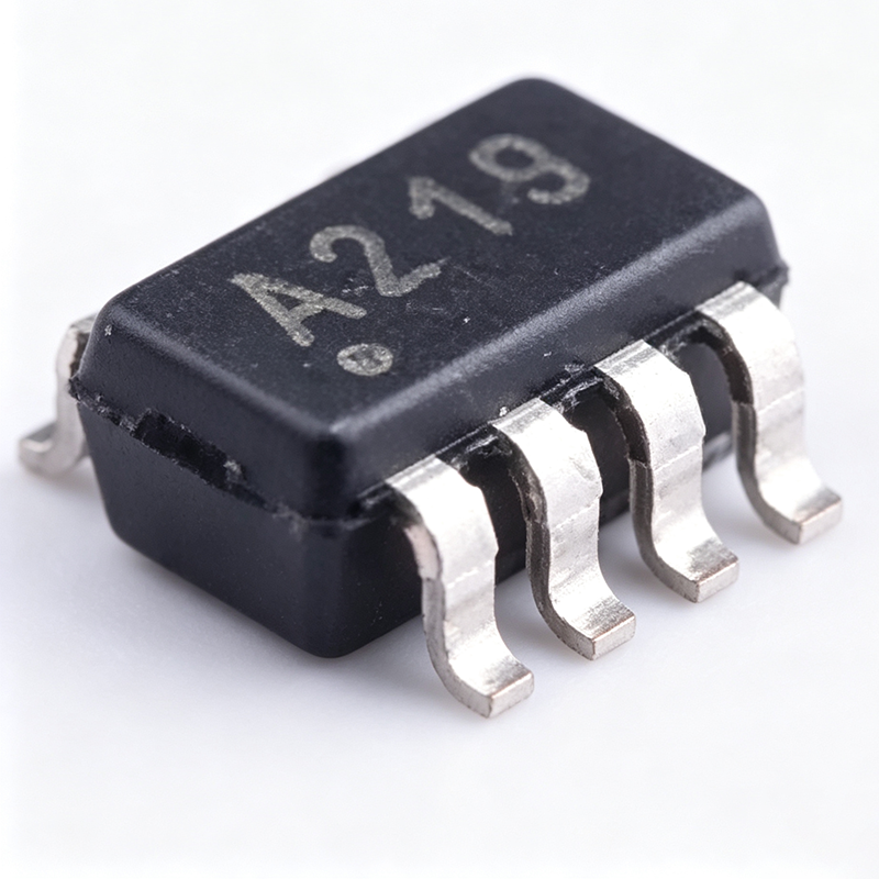
INA219AIDCNR - 26V 12-bit I2C Power Monitor | Texas Instruments
The Texas Instruments INA219AIDCNR is a zero-drift, bidirectional current shunt and power monitor with an I2C- or SMBus-compatible interface, packaged in a compact 8-pin SOT-23 (DCN) package. It measures both shunt voltage drop and bus supply voltage on buses from 0 to 26 V, operates from a single 3 V to 5.5 V supply, and draws a maximum of 1 mA of supply current. A current shunt monitor is an integrated circuit that measures the voltage across a sense resistor in series with a load, converting a small differential signal into a precise current reading. Within the power management IC hierarchy, current sense amplifiers such as the INA219 sit alongside voltage regulators and battery management ICs, providing the telemetry needed for system monitoring, protection, and efficiency optimization. The bidirectional architecture supports measurement of current flowing in both directions, which is essential for battery charge/discharge monitoring. Key features include a 12-bit ADC with programmable gain (0.125, 0.25, 0.5, and 1 V/V), a common-mode range of 0 to 26 V, 16 selectable I2C addresses via the A0/A1 pins, and a programmable calibration register combined with an internal multiplier enabling direct readouts of current in amperes and power in watts. The A grade provides an input offset of plus or minus 50 uV (max) and offset drift of plus or minus 0.5 uV/C (max). Technically, the zero-drift chopper-stabilized architecture maintains accuracy over the full -40C to +125C operating range. Programmable conversion time and averaging let engineers trade conversion speed against measurement noise, while optional filtering options improve reading stability in noisy switching environments. The SOT-23-8 package measures approximately 2.9 mm x 1.6 mm, suiting space-constrained designs. Typical applications include battery chargers, server power monitoring, telecom equipment, and power supplies, where accurate current and power telemetry is critical. It is also used in industrial load monitoring and fault detection systems. Design tip: place the shunt in the high-side path, decouple VS with a 0.1 uF capacitor close to the pin, and configure A0/A1 to avoid I2C address conflicts on the bus. This page synthesizes distributor pricing, drop-in alternatives, and practical design notes not found in the manufacturer datasheet.
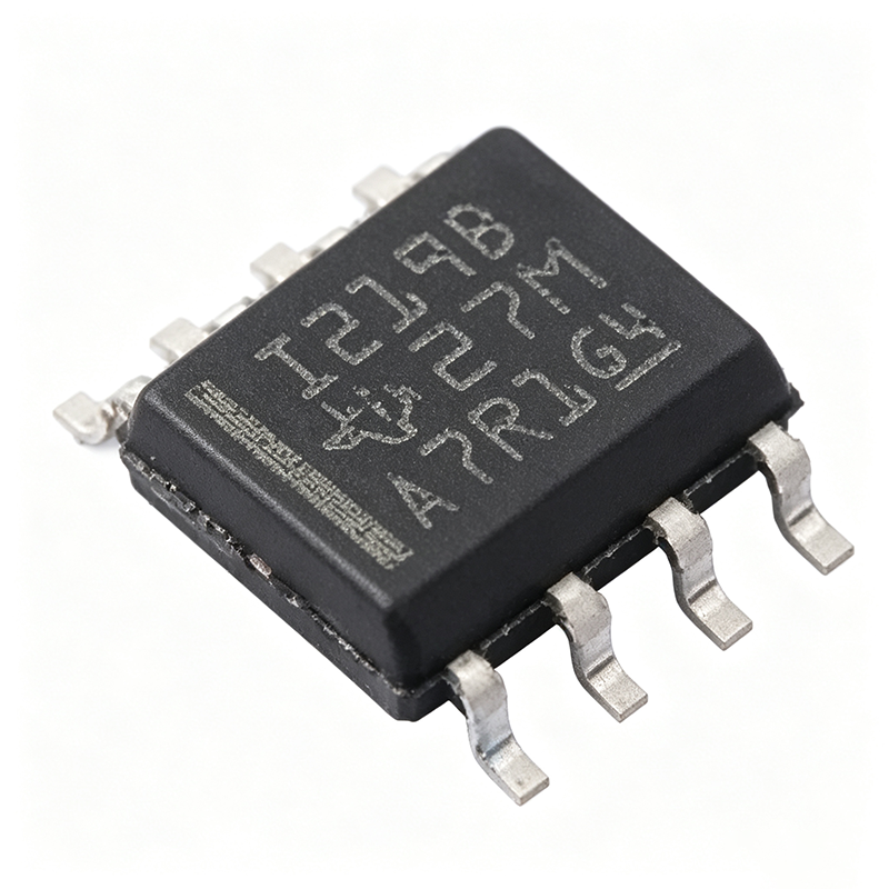
INA219BIDR - 26V 12-Bit I2C Power Monitor | Texas Instruments
The Texas Instruments INA219BIDR is a zero-drift, bidirectional current shunt and power monitor with an I2C- or SMBUS-compatible interface. It senses bus voltages from 0 to 26 V and reports current, voltage, and power through an integrated 12-bit ADC in an 8-pin SOIC package, operating from a single 3.0 V to 5.5 V supply drawing a maximum of 1 mA. The B grade offers 0.5% maximum accuracy over temperature. A current shunt monitor measures the voltage drop across a sense resistor placed in series with a load. The INA219BIDR is a digital power monitor, a subtype of current shunt monitor that integrates an ADC and digital interface to report current, voltage, and power directly to a microcontroller, fitting the hierarchy: current shunt monitor -> power monitor -> analog front-end -> signal chain IC. Key features include 16 programmable I2C addresses allowing up to 16 devices on one bus, programmable conversion times and filtering options, and a calibration register enabling direct readouts of current in amperes. An internal multiplier computes power on-chip, reducing host processor overhead. High-side sensing architecture monitors current without disturbing the ground path, critical for systems with shared grounds. The device uses a zero-drift architecture to minimize input offset voltage and drift, ensuring accuracy over temperature and time. The 12-bit ADC provides fine shunt-voltage resolution, enabling precise current sensing with minimal shunt resistance and low power loss. The I2C interface supports standard and fast modes with SMBus compatibility for server environments. Typical applications include server and telecom power management, battery chargers, embedded power supplies, test and measurement instruments, and industrial automation where accurate power telemetry is required. The 0 to 26 V bus range covers common 5 V, 12 V, and 24 V rails. Design tip: place the shunt resistor in the high-side path, keep bus voltage within 0-26 V, and use the ALERT-capable configuration to flag overcurrent events. Proper supply decoupling and short, Kelvin-connected shunt traces are essential for full 0.5% accuracy. Pricing from major distributors as of 2026-08-30.

INA223AIDSKR - 26V Zero-Drift Current Sense Amplifier | TI
The Texas Instruments INA223AIDSKR is a 26 V zero-drift, programmable-gain current shunt monitor and analog power monitor with voltage output, housed in a 10-pin WSON (DSK) package measuring 2.5 mm x 2.5 mm with exposed pad. It operates from a 2.7 V to 5.5 V supply and monitors shunt voltage at common-mode voltages from 0 V to 26 V. A current sense amplifier is a specialized differential amplifier that measures the voltage drop across a shunt resistor to derive load current, and often bus voltage and power, in a power rail. It sits within the power management IC hierarchy as a current and power monitoring device, distinct from regulators or converters because it measures rather than controls energy flow. High-side and low-side placement options let designers choose between ground-path integrity and load-drop immunity. Key features of the INA223AIDSKR include bi-directional current measurement, which supports both charging and discharging current monitoring in battery systems; zero-drift architecture, which minimizes offset drift over temperature for accurate readings; programmable gain, allowing a single shunt value to cover multiple current ranges; and simultaneous current, bus voltage, and instantaneous power outputs on analog pins. The zero-drift chopper-stabilized front end delivers DC accuracy that conventional amplifiers cannot match across the automotive-industrial temperature span, while the analog output interface allows direct connection to an ADC input or comparator without serial bus programming overhead. The 0 V to 26 V common-mode range makes the device tolerant of rail transients above its own 5.5 V supply. Typical applications include battery charge and discharge monitoring in portable equipment, server and telecom power rail supervision, and power-budget telemetry in industrial automation systems where analog outputs feed system controllers or watchdog circuits. Design consideration: choose the shunt resistance to balance full-scale drop (typically 50 mV to 100 mV at maximum load) against power dissipation, and use Kelvin connections at the shunt to preserve the accuracy offered by the zero-drift input stage. This page synthesizes distributor pricing, drop-in variant cross-references, and practical design notes not found in the manufacturer datasheet.