Batteriemanagement
Produkte (163)

315 - SR716SW Silver Oxide 1.55V Watch Battery | Energizer
The Energizer 315 is a silver-oxide button cell battery rated at 1.55 V nominal, with a diameter of 7.9 mm and a height of 1.65 mm, conforming to the SR716SW IEC designation. Housed in a sealed stainless-steel coin cell, it delivers a stable discharge curve optimized for low-drain analog watch movements, including conventional 3-hand quartz and slim dress watches. Silver-oxide watch batteries (chemistry code SR) are primary non-rechargeable cells that use a zinc anode and silver-oxide cathode, with alkaline electrolyte. Compared with alkaline button cells (LR) or mercury cells (former H prefix), silver-oxide chemistry provides a flatter voltage plateau throughout the discharge cycle, which keeps the watch movement's step-motor drive amplitude constant and prevents the "end-of-life slowdown" that alkaline cells exhibit. The SR716SW family occupies the niche between the smaller SR621SW (6.8 mm) and the larger SR916SW (9.5 mm). Key features include 1.55 V nominal voltage, 7.9 mm × 1.65 mm dimensions (per IEC 60086), leak-resistant sealed construction, and an operating temperature window of 0 °C to +60 °C. Capacity is approximately 22 mAh (per Energizer watch-cell datasheets), with a typical continuous drain of 30 µA at 1.5 V end-point for analog quartz movements. Shelf life is rated up to 5 years at +20 °C storage. Common alias part numbers include SR716SW, SR67, SR716, V315, D315, B315L, 530, 280-56, SB-AT, 614, HA, and the IEC code SR67. All share identical dimensions and voltage; only capacity may vary slightly between brands due to cathode formulation differences. Typical applications include analog quartz wristwatches, small digital timepieces, calculator backup cells, glucometer RTC backup, and low-power CMOS logic RTC retention. The thin 1.65 mm profile makes it the standard cell for slim dress watches with case thickness under 5 mm. Avoid mixing silver-oxide and alkaline watch cells in the same device - their voltage profiles differ and may cause erratic stepping. Store unused cells in original blister packaging to preserve shelf life and prevent inadvertent short-circuit on metal surfaces. This page consolidates the manufacturer-published cell dimensions, the cross-reference equivalency map, and known drop-in equivalents across brands not found in a single manufacturer datasheet.

ADBMS6948 - 16-Channel Battery Monitor | Analog Devices
The ADBMS6948 is a 16-channel battery pack monitoring system from Analog Devices, designed for measuring up to 16 series-connected battery cells with exceptional accuracy. It features the industry's first parallel measurement architecture, enabling simultaneous cell voltage and pack current measurements. The device achieves a total measurement error (TME) of less than 3 mV over the full temperature range and lifetime, making it suitable for demanding automotive and energy storage applications. The ADBMS6948 operates over a measurement range of -2.5V to 5.5V, supporting various battery chemistries including NMC and LFP. It is available in a 64-lead LFCSP-SS (9x9 mm) package. A battery pack monitoring system is an integrated circuit that measures the voltage, current, and temperature of individual cells in a battery pack to ensure safe and efficient operation. It is a critical component in battery management systems (BMS), which are used in electric vehicles, energy storage systems, and backup power supplies. The ADBMS6948 belongs to the category of battery monitoring ICs, which are part of the broader power management integrated circuit (PMIC) family. These devices provide essential data for state-of-charge (SoC) and state-of-health (SoH) estimation, cell balancing, and protection against overvoltage, undervoltage, and overcurrent conditions. Key features of the ADBMS6948 include synchronous pack current and cell voltage measurements, short/over current detection with less than 2 μs response time, programmable detection time and threshold, dedicated outputs for MOSFET/contactor control, redundant measurement, algorithm, and fault pin, 10 general-purpose I/O (GPIO) channels, cell and board temperature measurements, and pack, load, and system diagnostic measurements. The device also includes an SPI interface with a maximum operating frequency of [DATA_NEEDED: SPI max frequency] MHz, enabling high-speed communication with a host microcontroller. The ADBMS6948's parallel measurement architecture is a significant advancement over traditional sequential measurement systems, as it allows simultaneous sampling of all cell voltages and pack current, improving the accuracy of power and energy calculations. This is particularly important in applications where load transients can cause voltage fluctuations, as the synchronous measurement ensures that the voltage and current readings are time-aligned. The device also features a dedicated FAULTB pin that generates an interrupt when any preprogrammed over or under thresholds on cell voltage, cell temperature, or delta measurements are violated, providing immediate fault notification to the system controller. Typical applications for the ADBMS6948 include mild hybrid electric vehicles, two-wheeler and three-wheeler electric vehicles, four-wheeler electric vehicle auxiliary batteries, backup battery systems, and energy storage systems (ESS). Its high accuracy and robust feature set make it ideal for automotive battery management, where safety and reliability are paramount. The device's ability to measure both cell voltages and pack current synchronously enables precise state-of-charge estimation, which is essential for maximizing battery life and performance. When designing with the ADBMS6948, it is important to consider the PCB layout to minimize noise and ensure accurate measurements. The device requires careful decoupling of the power supply and proper grounding to achieve the specified TME. Additionally, the SPI interface should be isolated if the battery pack is at a high potential relative to the host controller, using components such as the ADuM1441ARWZ digital isolator. The ADBMS6948 is recommended for new designs, indicating that it is a current product with ongoing support from Analog Devices.

ATM90E26-YU-R - Single-Phase Energy Metering AFE | Microchip
The Microchip ATM90E26-YU-R is a single-phase high-performance wide-span energy metering analog front-end (AFE) IC designed for active and reactive energy measurement in single-phase two-wire, single-phase three-wire, and anti-tampering meters, packaged in a 28-pin SSOP with a built-in 8.192 MHz oscillator and 0.1% active energy measurement accuracy per the 8 ksps ADC chain. An energy metering AFE is a mixed-signal IC that combines high-resolution analog-to-digital converters (one for current, one for voltage), a digital signal processor for power calculations, and a serial host interface (SPI or UART) so an external microcontroller can read the computed active/reactive/apparent energy registers. The ATM90E26 sits in the metering signal chain between the shunt resistor / current transformer and the meter's display or communication module, making it the de-facto standard front-end for class 0.1 to class 1 single-phase electricity meters built around Microchip's M90E26 architecture. Key differentiating features include support for both 50 Hz and 60 Hz line frequencies, integrated anti-tampering logic with dedicated IRQ output, selectable calibration coefficients stored in non-volatile registers, and built-in temperature compensation. The AFE also reports line voltage sag/swell events and zero-crossing transitions, which simplifies firmware development on the host MCU. Its 2.8 V to 3.6 V supply range makes it compatible with common 3.3 V microcontrollers such as the PIC18 and SAM-D families. Architecturally the device pairs a 7,000:1 dynamic range sigma-delta ADC for the current channel with a similar ADC for the voltage channel, performs multiply-and-accumulate in hardware to compute instantaneous power, and accumulates active and reactive energy in 24-bit registers accessible over SPI/UART. Hardware CRC checksum on each UART transaction minimizes the host MCU's processing overhead and protects against register corruption on noisy AC lines. Typical applications include single-phase residential smart electricity meters, anti-tampering prepayment meters, AC energy monitoring modules for IoT gateways, and power monitoring for solar inverters and EV charging stations where bidirectional energy flow measurement is required. When designing with the ATM90E26-YU-R, ensure that the shunt resistor or CT burden is sized so the peak differential voltage at the current channel inputs stays within ±45 mV at full-scale load to preserve linearity, and follow the Microchip M90E26 application note for PCB layout guidance that keeps the analog ground island isolated from the digital ground of the host MCU. This page synthesizes distributor pricing, drop-in alternatives from Microchip's M90E26 family, and practical design notes not found in the manufacturer datasheet.

ATM90E32AS-AU - 3-Phase Energy Metering AFE | Microchip
The Microchip ATM90E32AS-AU is a high-performance three-phase energy metering analog front-end (AFE) IC with an integrated DSP for active, reactive, apparent and fundamental/harmonic energy computation, housed in a 48-pin TQFP (7x7 mm) package. The device measures voltage RMS, current RMS, mean active/reactive/apparent power and supports both three-phase four-wire (3P4W, Y0) and three-phase three-wire (3P3W, Y or Δ) topologies with selectable phase sequencing. An energy metering IC is a mixed-signal SoC that combines 7th-order sigma-delta ADCs, an embedded DSP, a precision on-chip voltage reference, and a calibration/manufacturing register bank in a single chip. It belongs to the broader category of power measurement ICs and sits hierarchically above discrete CT/PT + microcontroller solutions because it converts shunt/CT analog signals directly into calibrated digital energy and power quantities through SPI. Key features include an integrated DSP that computes active, reactive and apparent energy as well as voltage/current RMS and mean power, a four-wire SPI interface for host communication, and an on-chip high-precision reference voltage with low temperature coefficient. The measurement engine supports selectable gain and phase calibration registers so that CT phase error and shunt tolerance can be compensated in firmware, achieving better than Class 0.2S accuracy in production metering. Typical applications include three-phase four-wire (Y0) and three-phase three-wire (Y or Δ) static watt-hour meters, power monitoring instruments that measure voltage, current and mean power, and sub-metering modules for industrial PDUs, EV charging stations and solar inverters. The wide dynamic range and SPI interface also make it popular in DIY open-source energy monitors built on ESP32 hosts. When designing with this part, note that the IC cannot drive a burden resistor directly - an external anti-aliasing RC network and shunt resistors (or current transformers) must be selected to match the expected line current. PCB layout should keep the analog ground island small and place decoupling capacitors within 3 mm of each supply pin to meet conducted EMI and surge requirements. This page synthesizes distributor pricing, drop-in alternative MPNs, and practical design notes that are not collected in any single manufacturer datasheet, helping BOM engineers and firmware developers shortlist parts faster.
ATM90E36A-AU-Y - 3-Phase Energy Meter IC, 48-TQFP | Microchip
The Microchip ATM90E36A-AU-Y is a high-performance, poly-phase energy metering IC for three-phase four-wire (3P4W, Y0) and three-phase three-wire (3P3W, Y or Delta) systems, packaged in a 48-pin TQFP (7x7 mm) with industrial temperature grade (-40C to +85C) and 1.8V/3V supply rails. The device integrates seven input channels (three voltage, three current, and one neutral) with 24-bit sigma-delta ADCs, on-chip DSP, and a SPI/UART host interface, providing active, reactive, and apparent energy plus voltage/current RMS, line frequency, power factor, THD, and per-phase temperature measurement. An energy metering IC is a mixed-signal system-on-chip that samples voltage and current waveforms on AC power lines and computes billing-grade quantities (kWh, kVArh) plus power-quality metrics in firmware/hardware rather than via an external DSP or MCU. Energy metering sits hierarchically inside power management ICs (PMIC), which in turn belong to the broader category of analog/mixed-signal data acquisition and signal conditioning semiconductors. The ATM90E36A's built-in FFT/Fourier analysis, harmonic measurement (up to 21st harmonic typical for parts in this family), and per-phase temperature compensation let it stand alone in low-cost data acquisition terminals without an external DSP. Key features include <0.1% active/reactive energy accuracy (typical) on the ATM90E36A platform, integrated anti-tamper detection on the neutral line, a proprietary SPI frame format for parameter read/write, calibration registers in internal non-volatile memory (or via host MCU), and selectable 3.3V or 1.8V digital interface. The wide dynamic range of the current channel allows a single design to cover 1A to 100A CT or shunt loads with appropriate scaling. Compared to discrete energy-meter solutions using an external ADC plus an MCU, the ATM90E36A reduces BOM cost, simplifies certification (IEC 62053-22/23 class 0.2S-grade variants are supported in the family), and shortens time-to-market. Typical applications include three-phase smart energy meters (residential, commercial, industrial), sub-metering for data centers and building automation, EV charging station metering per IEC 61850/IEEE 1459, solar inverter AC-side export/import monitoring, and power monitoring instruments that report per-phase voltage/current/THD/mean power. The on-chip temperature sensor also enables inside-the-enclosure thermal monitoring for the meter itself. When designing with this device, allocate at least one layer of the PCB ground plane for the analog ground island, place the 0.1 uF + 10 uF decoupling pair close to AVDD/DVDD pins, and shield the SPI traces from the high-voltage CT/PT sense traces with a guard ring tied to AGND. Calibration is via software-only register writes; no external trim parts are required. This page synthesizes XAIPART-sourced distributor pricing, drop-in same-brand and cross-brand alternatives, and practical design notes not found in the manufacturer datasheet alone.
BCM59011B0KMLG - PSE 30W+ Octal PoE Controller | Broadcom
The Broadcom BCM59011B0KMLG is a Power Sourcing Equipment (PSE) Power over Ethernet (PoE) controller IC delivering 30 W+ per port, classified in the PMIC - Power over Ethernet (PoE) Controllers category and described by distributors as a PSE 30W+ OCTAL POE device with single-channel controller function. A Power over Ethernet PSE controller is a power management IC that sits in the powered device port of network switches and midspans. It negotiates power with the connected powered device (PD), classifies the load, monitors current and voltage, and disconnects faulty ports - forming the power-delivery layer of the power management IC hierarchy alongside regulators and battery management ICs. Key features include its 30 W+ power-per-port capability, which supports higher-power PoE classes used in access points, IP cameras, and industrial endpoints, and its octal-port system-level designation (PSE 30W+ OCTAL POE), indicating deployment in multi-port PoE switching infrastructure where eight channels are managed as a group. According to Octopart's parameter comparison, the device is categorized as Type: Controller (PSE), Number of Channels: 1, Power - Max: 30 W, and Internal Switch(s): No, meaning an external MOSFET switch stage is required in the power path. Because the internal switch is not integrated, designers pair the BCM59011B0KMLG with external pass devices and sense resistors, which gives flexibility in thermal design but adds board area. The single-channel controller architecture is typically replicated across the ports of an octal system, sharing supervisory and sequencing logic. Typical applications include enterprise PoE switch line cards, PoE midspan injectors, wireless access point infrastructure, and surveillance camera power distribution where 30 W-class power negotiation and fault isolation are required. A key design consideration is the external switch selection: the external MOSFET must handle the 30 W-class current with adequate RDS(on) and SOA margin, and current-sense accuracy directly affects PoE classification compliance. This page synthesizes distributor inventory data, Octopart parameter comparisons, and drop-in alternative analysis not found in the manufacturer datasheet alone.
BQ21061YFPR - 500mA 1-Cell Linear Charger 10nA Ship | TI
The Texas Instruments BQ21061YFPR is an I2C-controlled, 1-cell, 500-mA linear battery charger with 10-nA ship mode, integrated power-path with regulated PMID system voltage, and a low-dropout (LDO) post-regulator, all packaged in a 20-ball DSBGA (YFP) chip-scale package. The device charges single-cell Li-Ion or Li-Polymer batteries from a 3.9V to 6.45V input source and supplies a regulated 3.5V to 4.4V PMID output to the system load while simultaneously charging the battery. A battery charger IC is a specialized power management device that converts an external DC source (USB, wireless, solar, or adapter) into a precise current/voltage profile tailored to a battery's chemistry, while protecting the cell from over-voltage, over-current, and thermal stress. Linear chargers - as opposed to switching chargers - dissipate the excess VIN-VBAT voltage as heat, which makes them simpler, smaller, and noise-free, but limits their use to sub-1A applications where the thermal budget is acceptable. The BQ21061 sits at the high end of TI's nano-power charger family: 10-nA ship-mode quiescent current extends shelf life for years on primary cells, and the integrated PMID power-path allows the system to boot and run from the input source even with a deeply discharged or absent battery. Key features include programmable charge current up to 500 mA, ±0.5% battery regulation accuracy across -40°C to +85°C, dynamic power-path management (DPPM) that adjusts charge current to maintain PMID regulation, a programmable termination current down to 1 mA, and a thermal-regulation loop that automatically reduces charge current at high junction temperatures. The integrated 50-mA LDO can supply a clean rail to always-on peripherals (RTC, sensors, MCUs in sleep). The BQ21061 uses a switched-mode-style architecture on the charger section with a high-side P-channel FET pass element, a precision bandgap reference, and an 8-bit DAC for current/voltage programming over I2C. The PMID rail is regulated via a separate linear LDO controller and supports dynamic load sharing between input source, battery, and system load, ensuring no back-feed to the USB port. Typical applications include wearables (TWS earbuds, smartwatches, fitness bands), hearables, IoT sensor nodes, low-power medical patches, and any single-cell Li-Ion design that needs <100 nA quiescent current for multi-year storage. The wide VIN range (3.9V-6.45V) is fully compatible with USB, 5V adapters, and solar panels with MPPT front-ends. Design trade-off: because the charger is linear, total power dissipation = (VIN - VBAT) × ICHG. At 500 mA and VIN = 5V with a 4.2V battery, the device dissipates ~0.4W; designers must ensure the DSBGA thermal pad is soldered to a copper pour with thermal vias to avoid triggering the thermal-regulation loop unnecessarily. I2C address (default 0x6B) must be checked against any other charger on the same bus. This page synthesizes distributor pricing, drop-in alternatives from the BQ2106x family, and practical design notes not found in the manufacturer datasheet.
BQ21061YFPT - 500mA 1-Cell Linear Charger w/ 10nA Ship Mode | TI
The Texas Instruments BQ21061YFPT is a 500-mA I2C-controlled 1-cell linear battery charger with 10-nA ship mode, integrated power-path management, regulated system (PMID) voltage, and a built-in LDO, all integrated into a 20-ball DSBGA (YFP) package. It supports Li-Ion/Li-Polymer cells and provides a programmable charge current up to 500 mA with safety timers and thermal regulation, making it suitable for compact wearables, hearables, and IoT sensor nodes where PCB real-estate is severely constrained. The integrated power-path allows the system to operate directly from PMID while the charger simultaneously refuels the battery. A linear battery charger is a power management subcircuit which regulates charging current/voltage into a single-cell Li-Ion/Li-Polymer battery using a series pass element. Within the broader system taxonomy, a linear charger sits below a switching charger and below a power management IC, providing the safest and lowest-EMI charging path for small batteries at the cost of higher conduction dissipation. The BQ21061 specifically targets ultra-low-power IoT devices by combining charger + power-path + LDO in a single die, eliminating the need for a separate PMIC in simple wearable designs. Key features include a 10-nA ship mode quiescent current that dramatically extends shelf life on the warehouse shelf and during end-user storage, I2C programmability for charge current, input current limit, charger enable, and safety timers, integrated power-path with PMID regulation that allows system operation even with a deeply discharged or absent battery, and an integrated LDO that can supply low-voltage always-on rails for the host MCU. The 20-ball DSBGA package measures approximately 1.6 mm x 2.0 mm, enabling direct placement in space-constrained wearable form factors. The BQ21061 is engineered around a low-Rdson pass transistor architecture with an integrated sense resistor, providing high-accuracy charge current regulation and thermal management. Thermal regulation automatically reduces charge current at elevated die temperatures, protecting the device and battery in thermally constrained designs. The I2C interface allows host processors to dynamically adjust parameters and read status flags including charging state, fault conditions, and battery voltage. Typical applications include TWS earbuds charging cases, fitness bands, smart watches, IoT sensor nodes, Bluetooth trackers, and medical wearables such as continuous glucose monitors and pulse oximeters. Its combination of low quiescent current, small package, and integrated power-path makes it ideal for battery-powered products that must run for months on a single charge. When integrating this device, designers should follow TI reference layout guidance for the DSBGA thermal pad to ensure adequate heat dissipation during fast-charge at high VIN-VBAT differentials.
BQ24133QRGYRQ1 - 2.5A 1-3 Cell Buck Charger Q1 | TI
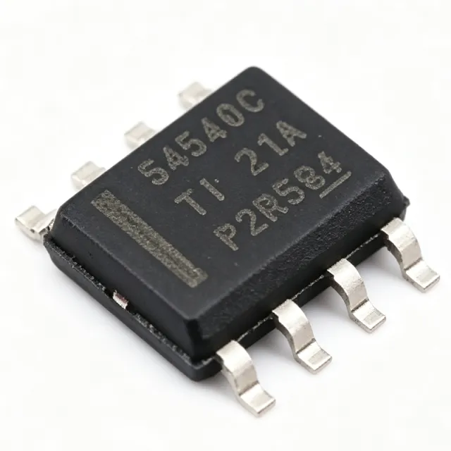
The Texas Instruments BQ24133QRGYR is an automotive-grade (AEC-Q100) stand-alone 1.6-MHz synchronous switched-mode Li-Ion and Li-Polymer battery charger with two integrated N-channel power MOSFETs, delivered in a 24-pin VQFN (RGY, 5.5x3.5 mm) package. It charges 1-cell, 2-cell, or 3-cell battery stacks at up to 2.5 A with a regulated 4.2 V/cell charge voltage. A switched-mode battery charger is a DC-DC converter-based power management IC that regulates charge current and battery voltage with far higher efficiency than linear chargers. Within the power-management IC hierarchy, the BQ24133 family sits between a generic buck regulator and a full battery management IC, adding charge termination, thermal regulation, and adapter-to-battery power path selection. Key features include a 1.6-MHz constant-frequency synchronous PWM controller delivering up to 92% efficiency, a 30-V input rating with adjustable input overvoltage protection, a 4.5-V to 17-V operating input range, and an automatic power path selector between the adapter and battery. High-accuracy regulation of input current, charge current, and charge voltage enables the device to safely work with limited-adapter-power systems, while dynamic power management protects overloaded sources. The device closely monitors battery pack temperature (TS pin with NTC) and permits charging only within a preset temperature window, an essential safety behavior for automotive and industrial lithium batteries. Integrated MOSFETs eliminate external discrete transistors, shrinking the solution footprint and reducing BOM count. Typical applications include automotive infotainment and telematics backup batteries, industrial handheld instruments, portable medical devices, and battery-backed servers or gateways requiring seamless adapter-to-battery transition. The power path feature keeps the system alive even with a deeply discharged battery. Design consideration: the 1.6-MHz switching frequency permits small inductors, but PCB layout of the power loop must be tight; place the inductor, input capacitor, and PGND connections per the datasheet layout guidelines to minimize EMI.

BQ24133RGYR - 2.5A 1.6MHz Sync Buck Charger | TI
The Texas Instruments BQ24133RGYR is a highly integrated stand-alone Li-Ion and Li-Polymer switched-mode battery charger with two integrated N-channel power MOSFETs. It operates as a 1.6-MHz synchronous buck charger delivering up to 2.5A charge current for 1-3 cell battery packs, housed in a 24-pin VQFN (RGY) package measuring 5.5x3.5 mm for space-constrained portable designs. A battery charger IC is a power-management device that safely controls charging current and voltage for rechargeable cells. The BQ24133 uses a synchronous buck converter topology to step down input voltage efficiently, minimizing heat compared to linear chargers. It belongs to the battery management IC hierarchy within power management semiconductors, essential for portable electronics, tools, and medical devices. Key features include high-accuracy regulation with plus/minus 1% charge voltage accuracy, a wide input range from a DC source as high as 17V including automotive car batteries, and an adjustable input overvoltage limit via the OVPSET pin with 30V rating on AVCC, ACP, and ACN pins. An integrated power path selector lets the system run from the adapter while charging the battery, and an external thermistor enables charging only within a safe temperature window. Technically, the constant-frequency synchronous PWM controller at 1.6 MHz permits small inductors and capacitors. Charge current is programmable via an external resistor, and cell count is configured for 1, 2, or 3 series cells. Thermal regulation reduces charge current when die temperature exceeds threshold, and a low-power sleep mode minimizes battery drain when input is removed. On high-voltage DC insertion, Q1 and Q2 remain off to protect the system. Typical applications include smartphones, tablets, digital cameras, power banks, solar-powered chargers, battery-powered industrial equipment, and medical devices. Design tip: ensure adequate copper pour for thermal dissipation and place input/output capacitors close to the IC; select the inductor based on the 1.6-MHz switching frequency to minimize ripple.
BQ24193 - I2C 4.5A Single-Cell USB/Adapter Charger | Texas Instruments
The Texas Instruments BQ24193 is an I2C-controlled, 4.5 A single-cell Li-Ion/Li-Polymer battery charger with narrow VDC power-path management and USB On-the-Go (OTG) boost operation, housed in a 24-pin 4 mm x 4 mm thin VQFN (RGE) package. The device integrates a switch-mode charger, input current and voltage regulation compliant with USB 2.0/USB 3.0 power specifications, system power-path management, and a synchronous boost converter that delivers 5 V on VBUS up to 1.3 A for OTG accessories. A switch-mode battery charger (SMBC) is a power management IC that converts an external supply (USB, adapter, or wireless) into a precisely regulated charging profile for a lithium-based cell while simultaneously managing the dynamic power path between the adapter, the system load, and the battery. Within the power-management hierarchy, it sits one level above simple linear chargers because its synchronous buck topology sustains high efficiency across wide VIN/VOUT ratios, reducing heat dissipation in space-constrained portable designs. Key features include a programmable charge current up to 4.5 A, ±0.5% battery regulation accuracy, 20 V tolerant input with overvoltage protection, configurable thermal regulation thresholds, and an I2C interface for charge-parameter programming, status telemetry, and interrupt reporting. The narrow-VDC topology keeps VBUS just above VBAT during system load transients, minimizing adapter current overshoot while extending adapter compatibility. Architecturally, the BQ24193 pairs a synchronous buck charger with a boost controller sharing the same power-stage pins, enabling seamless OTG reverse operation without external MOSFETs. Integrated input-current sensing, dynamic power-path management (DPPM), and JEITA temperature monitoring reduce external component count by typically 15-20 components versus discrete solutions, making the part well suited to compact tablet, ultrabook, and power-bank designs. Typical applications include single-cell Li-Ion tablets, ultrabook charging sub-systems, USB-PD/QC adapter charging, portable medical monitors, and OTG-capable power banks that supply 5 V to downstream accessories. Engineers commonly pair the BQ24193 with a USB Type-C PD controller on the input side and a Li-Ion gauge IC on the battery side. A key design consideration is thermal management: at VIN = 9 V, VBAT = 4.2 V, and ICHARGE = 3 A, the device dissipates an estimated 14 W. Designers should compute PCB copper area against the datasheet theta_JA value and add thermal vias under the exposed pad to keep Tj below 125 C. Charge-parameter defaults in non-volatile memory should be configured before production to prevent undefined behavior on first power. This page synthesizes distributor pricing, verified drop-in alternatives in the BQ2419x family, and practical design notes not consolidated in the manufacturer datasheet, helping engineers shorten their evaluation cycle.
BQ24251RGER - 2A I2C Li-Ion Charger IC | Texas Instruments
The Texas Instruments BQ24251RGER is a 2A single-input, I2C/standalone switched-mode Li-Ion battery charger with power-path management, housed in a 24-pin VQFN (4x4 mm) package. It integrates a high-efficiency synchronous buck charger, power-path management, and USB/BC1.2 detection, enabling efficient charging from USB or AC adapters while powering the system independently of battery presence. A battery charger IC is a power management device that regulates the charging of rechargeable batteries, ensuring safe and efficient energy transfer. The BQ24251 belongs to the battery charger IC family, which falls under battery management ICs, a subset of power management integrated circuits (PMICs). These devices are essential in portable electronics, where they manage charge current, voltage, and thermal conditions to extend battery life and ensure safety. Key features include a selectable input current limit of 100 mA, 500 mA, 900 mA, 1.5 A, and 2 A, USB charging compliance, BC1.2-compatible D+/D- detection in host mode, and a separate power path that allows system startup from a deeply discharged or missing battery. The I2C interface enables dynamic control of charge parameters, while standalone mode supports autonomous operation without host intervention. The BQ24251 uses a switched-mode architecture with a high-efficiency synchronous buck converter, achieving up to 92% efficiency. It integrates power-path management, which prioritizes system load over battery charging, reducing battery cycling and enabling instant-on functionality. The device also includes safety features such as thermal regulation, overvoltage protection, and a watchdog timer. Typical applications include smartphones, tablets, portable media players, and other USB-powered devices. Its power-path management makes it ideal for applications requiring instant system operation even with a depleted battery, such as GPS units and handheld medical devices. When designing with the BQ24251, ensure proper PCB layout with adequate ground plane and input/output capacitor placement to minimize noise and optimize thermal performance. The I2C address and charge parameters should be configured according to the system requirements, and the watchdog timer must be serviced in host mode to avoid unintended shutdown.
BQ24295RGER - 3A I2C Single-Cell USB Charger | Texas Instruments
The Texas Instruments BQ24295RGER is an I2C-controlled 3 A single-cell Li-Ion / Li-Polymer battery charger with USB 2.0 / USB 3.0 input current and voltage compliance, packaged in a 24-pin VQFN (RGE) 4x4 mm footprint. The device supports narrow-VDC operation at 4.5-5.5 V input and includes an integrated 1.5 A synchronous boost OTG output. According to the TI datasheet, the bq24295 detects the input source through D+/D- following the USB Battery Charging Specification 1.2 and recognises non-standard 2 A / 1 A adapters. Programmable thermal regulation, power-path management, and an I2C interface for charge current / voltage / status make it a complete power-management solution for portable hosts that draw charge from a USB port or wall adapter. What is an I2C-controlled single-cell Li-Ion charger IC? It is a battery charger integrated circuit that communicates with a host microcontroller via the I2C (Inter-Integrated Circuit) serial bus, allowing the system to read status, set charge current, and modify termination thresholds in real time. Single-cell means it charges one Li-Ion / Li-Polymer cell (typically 3.0 V to 4.2 V), as opposed to multi-cell packs that require higher stack voltages. Within the broader taxonomy, the BQ24295 belongs to battery chargers -> battery management -> power management IC -> semiconductor. Key features include: up to 3 A continuous charge current, programmable charge voltage, dynamic power-path management (PPM) that shares current between system load and the battery, an integrated 1.5 A boost converter for OTG (On-The-Go) 5 V output to power accessories, and JEITA-compliant battery temperature monitoring that adjusts charge voltage and current across cold / cool / warm / hot ranges. The VQFN-24 package exposes a thermal pad that drops the junction-to-ambient thermal resistance to a level sufficient for the device's 2 W typical dissipation at 2 A charge. The BQ24295 uses a synchronous switch-mode charger topology with an internal power MOSFET pair to deliver high efficiency (> 90% at 2 A charge), which reduces package temperature rise versus linear chargers. Dynamic power-path management arbitrates input-current demand between the system load and the battery, allowing the system to boot even with a deeply discharged battery, then seamlessly transfers to charge mode as input power becomes available. The IC also supports input current limiting with up to 3 A detection, USB OTG boost output, and watchdog-protected I2C communication. Typical applications include smartphones, tablets, portable medical devices, Bluetooth speakers, GPS / asset trackers, power tools, and any single-cell Li-Ion system that draws from USB or 5 V adapter sources. The device's small 4x4 mm VQFN-24 footprint is ideal for space-constrained PCB designs. When designing with the BQ24295, ensure the input capacitor (>= 4.7 uF) and output capacitor (>= 10 uF) follow the datasheet guidance, keep the SW node short and surrounded by a thermal pour, and use the I2C bus to dynamically adjust charge current based on the input source type (USB SDP / CDP / DCP, or proprietary adapters). The thermal pad MUST be soldered to a sufficiently large copper plane for reliable operation at the 3 A fast-charge rating. This page synthesises distributor pricing for the BQ24295RGER (TI), pin-compatible same-family drop-in alternatives, and practical thermal / PCB layout notes not duplicated from the manufacturer datasheet.
BQ24610QRGERQ1 - 1-6 Cell Buck Battery Charger Q1 | Texas Instruments
The Texas Instruments BQ24610QRGERQ1 is an AEC-Q100 qualified, stand-alone synchronous switch-mode battery charge controller for 1- to 6-cell Li-ion and Li-polymer batteries, housed in a 24-pin VQFN (RGE, 4x4 mm) package. As part of the automotive-grade BQ2461x-Q1 family, it drives external N-channel MOSFETs in a synchronous buck topology for high-efficiency charging. A battery charge controller is a power management IC that regulates current and voltage delivered to rechargeable cells. The BQ24610 manages the full charge profile: preconditioning (trickle charge for deeply discharged cells), constant-current (CC) fast charge, constant-voltage (CV) regulation, and charge termination, with automatic recharge when the battery voltage falls below the recharge threshold. Key features include a constant-frequency current-mode PWM controller with high-accuracy charge current and voltage regulation (0.5% charge voltage accuracy), an integrated system power selector (NVDC-style power path) that allows the system to boot from the adapter even with a deeply discharged or absent battery, adapter current regulation to prevent adapter overload, and low quiescent current for efficiency. Charge status outputs and safety timers provide monitoring and fault protection including thermal shutdown and battery temperature qualification via TS pin (JEITA-style NTC monitoring). The controller architecture keeps power losses in external components, enabling charge currents of several amperes set by the external sense resistor, with programmable switching frequency for inductor and MOSFET optimization. Input voltage operating range supports common automotive and adapter rails up to 28 V. Typical applications include automotive infotainment and telematics backup batteries, portable industrial instruments, medical handheld devices, and 1-6 cell battery-powered systems requiring power-path management. For a non-automotive equivalent, the BQ24610RGER shares the same die and footprint. Design tip: size the sense resistor for the target fast-charge current (Rsense = 50 mV / Ichg typical), and follow the TI datasheet layout guidelines to place the bootstrap capacitor, gate-drive loops, and NTC network close to the IC for robust synchronous buck operation.
BQ24610RGER - Stand-Alone Sync Li-Ion Battery Charger | TI
The Texas Instruments BQ24610RGER is a highly integrated, stand-alone synchronous switch-mode battery charge controller for Li-ion, Li-polymer, and lead-acid batteries, housed in a 24-pin VQFN (4x4 mm, RGE) package with exposed thermal pad. It supports up to 6 cells in series and delivers high-accuracy charge current and voltage regulation with system power selector functionality. A battery charge controller is a power management IC that regulates charging of rechargeable batteries, managing charge current, voltage regulation, preconditioning, and termination for safety and battery longevity. The BQ24610 belongs to the switched-mode charger family within the broader power management IC hierarchy, using a constant-frequency synchronous PWM controller to achieve far higher efficiency than linear chargers, which reduces heat dissipation in space-constrained designs. Key features include a constant-frequency synchronous buck PWM controller with external MOSFETs for charge currents up to 10 A, high-accuracy regulation (0.5% charge voltage accuracy), adapter current regulation (input DPM), and charge status monitoring. Three-phase charging - preconditioning, constant current, and constant voltage - maximizes battery life. A system power selector allows the system load to run from the adapter or battery, while low quiescent current conserves battery energy during storage. Technically, the BQ24610RGER implements a proprietary voltage regulated loop with programmable termination, safety timers, thermal regulation, and fault protection. Synchronous rectification reduces conduction losses; the controller architecture keeps external FETs off-package, allowing charge current to be scaled to the application needs. Stand-alone operation requires no host microcontroller for basic charging functions, simplifying system design. Typical applications include notebook and tablet power banks, portable instruments, power tools, ePOS terminals, and medical devices requiring continuous system operation during charging (power path management). Design tip: ensure proper PCB layout with thermal vias under the exposed pad, place the charge current sense resistor near the IC to reduce noise, and set the input DPM threshold to match the adapter rating to prevent adapter overload. Pricing shown reflects estimates as of 2026-08-29.
BQ25601RTWR - 3A I2C Buck Battery Charger | Texas Instruments
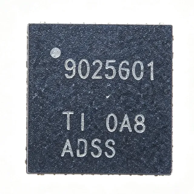
The Texas Instruments BQ25601RTWR is a highly integrated I2C-controlled 3A single-cell battery charger with Narrow Voltage DC (NVDC) power path management, designed for high input voltage applications. It operates from an input voltage range of 3.9V to 13.5V (14V absolute maximum) and supports a charge current up to 3A, in a 24-pin WQFN (4x4mm) RTW package over -40C to +85C. A battery charger IC is a power management integrated circuit that regulates the charging of rechargeable batteries, ensuring safe and efficient charging while protecting the battery from overvoltage, overcurrent, and overtemperature conditions. Within the power management IC hierarchy, the BQ25601 integrates a synchronous buck converter, NVDC power path management, and an I2C interface, enabling dynamic power management between the input source, system load, and battery. This allows the system to boot and operate even when the battery is deeply discharged or absent. Key features include a 3A fast-charge current, adjustable charge voltage from 3.856V to 4.624V, high input voltage support up to 13.5V, and an integrated bootstrap diode for the high-side gate drive that simplifies system design and reduces BOM count. The I2C serial interface provides programmable charge current, charge voltage, and input current limits, and supports On-The-Go (OTG) boost operation from the battery to power attached USB peripherals. The BQ25601 uses a synchronous buck topology with a high-efficiency power stage, achieving approximately 92% efficiency at typical operating conditions. Input voltage and current regulation (DPM) deliver maximum charging power from USB adapters and other sources, while protections include input overvoltage, battery overvoltage, and thermal shutdown. Typical applications include smartphones, tablets, portable speakers, power banks, and industrial or medical handheld devices requiring reliable high-current single-cell charging with power path management. When designing with the BQ25601, ensure a proper PCB layout with thermal vias under the exposed pad and adequate copper area for heat dissipation at 3A charge currents, and configure I2C registers to set the desired charge parameters. According to TI datasheet (bq25601.pdf), pricing at authorized distributors starts around $0.37 at LCSC as of 2026-08-30.

BQ25703ARSNR - I2C 1-4 Cell NVDC Buck-Boost Charge Controller | TI
The Texas Instruments BQ25703ARSNR is an I2C-controlled, multi-chemistry, 1-to-4 cell NVDC buck-boost battery charge controller with system power monitor and processor hot monitor, housed in a 32-pin WQFN (RSN) 4x4 mm package. It accepts a wide input voltage range of 3.5V to 24V (with 36V absolute maximum transient tolerance on VBUS) and delivers up to 6.35A continuous charge current to the battery, while supplying the system load directly through the integrated NVDC power path. The part supports Li-Ion, Li-Polymer, LiFePO4, lead-acid, NiMH, NiCd and supercapacitor chemistries over the 1.024V to 19.2V battery range. A buck-boost battery charge controller is a power-conversion and power-path-management IC that accepts an input source voltage that may be higher, lower, or equal to the battery voltage, and continuously regulates the charge current and voltage into a multi-cell series battery pack. As a category, it sits within the battery management IC (BMIC) family, itself a subset of power management ICs that handle charging, gauging, protection and authentication for rechargeable energy storage. The BQ25703A family specifically targets USB-C PD, two-port adapter and wide-Vin industrial charging applications that require seamless source/battery load-sharing. Key features of the BQ25703ARSNR include integrated charge, system, and recharging FETs, 1.5MHz programmable switching frequency, integrated 12-bit ADC for voltage, current and temperature telemetry, dynamic power-path management (DPPM) for adapter load sharing, and USB-C PD negotiated-input support up to 20V through the integrated input-current optimizer. The IC also includes a processor hot-monitor function that flags system overheating via I2C status bits and a JEITA-compliant thermal regulation loop that throttles charge current to maintain safe cell temperature. The device uses a peak-current-mode buck-boost architecture with four MOSFETs and an inductor, allowing the converter to operate seamlessly across boost (VIN < VBAT), buck (VIN > VBAT), and pass-through (VIN = VBAT) regions without mode-transition artifacts. The NVDC topology keeps the system rail just above VBAT when input is absent, allowing instant turn-on when the adapter is plugged back in, while the input current optimizer regulates adapter draw to within USB-C PD negotiated limits with sub-100 mA accuracy. Typical applications include 1S to 4S USB-C PD laptop power banks, 2-in-1 detachable notebook chargers, 12V industrial sensor backpacks with supercapacitor buffering, USB-PD multi-port hubs that charge attached devices, and portable medical carts using LiFePO4 battery stacks. The wide chemistry support also makes it suitable for e-mobility kick-scooter and e-bike on-board chargers operating from 36V ebike-bus supplies. When designing with this device, ensure that the input bulk capacitor, the four buck-boost switching-node snubbers, and the battery-side sense resistor are sized per the BQ25703A datasheet typical-application circuit. The PROG pin resistor sets the default battery charge current before any I2C override, and the ILIM pin programs the adapter-side current limit. Both must be populated even when I2C defaults are used. This page synthesizes distributor pricing, drop-in WQFN-32 alternatives, I2C register differences and practical design notes not found in the manufacturer datasheet alone.

BQ25703ARSNT - NVDC Buck-Boost Battery Charger | Texas Instruments
The Texas Instruments BQ25703ARSNT is a synchronous NVDC (narrow-voltage DC) I2C-controlled multi-chemistry buck-boost battery charge controller with system power monitor and processor hot monitor, housed in a 32-pin WQFN (RSN) 4x4 mm package with small 250-unit tape-and-reel packaging. The device charges 1- to 4-cell battery packs from a wide 3.5V to 24V input source (adapters, USB-C PD, solar) and supports multi-chemistry profiles including Li-Ion, LiFePO4, Lead Acid, NiCd, and NiMH. Maximum charge current reaches 8.128A at up to 19.2V output, enabling fast-charging high-capacity packs. The IC integrates a buck-boost topology that delivers seamless transition between boost and buck modes without disturbing the system rail. A buck-boost battery charger is a switching-mode power controller that can either step up (boost) or step down (buck) its input voltage to maintain a regulated output for charging multi-cell battery stacks, regardless of whether the input is above or below the battery voltage. Within the power management hierarchy, the BQ25703A sits at the battery management sub-category alongside fuel gauges and protectors, and within the broader category of battery charging ICs. Its NVDC-1 configuration regulates the system rail at battery voltage but never below a programmable minimum, allowing operation even when the battery is fully depleted. Integrated power-path MOSFET drivers and a high-accuracy 16-bit ADC enable compact, high-efficiency designs. Key features include integrated charging, a system power monitor with input current/voltage MPPT support, a processor hot monitor for thermal throttling signals, and an I2C host interface for telemetry and configuration. The switching frequency is programmable up to 1.5 MHz, enabling small external inductors. Built-in protections cover input overvoltage, battery overvoltage, overcurrent, thermal shutdown, and safety timer. The small WQFN-32 (RSN) footprint suits space-constrained USB-C PD laptops, drones, power tools, and industrial battery packs. The BQ25703A uses a synchronous buck-boost topology with high-side and low-side MOSFET gate drivers and supports both adapter and battery as the system power source. Its NVDC architecture maintains a minimum system voltage (VSYS_MIN) during battery transients, preventing CPU brownouts. The 16-bit ADC provides accurate measurements of input voltage, input current, battery voltage, battery current, system voltage, and die temperature. The integrated MPPT algorithm and processor hot monitor are differentiated features rarely combined in competing parts. Typical applications include 2S-4S USB-C PD laptop chargers, power tool battery packs, drone charging hubs, solar power bank controllers, and portable industrial test equipment. The wide-chemistry and 1-4 cell flexibility make it broadly deployable across consumer and industrial energy storage products. When designing with the BQ25703A, ensure the input capacitor (CIN) and decoupling capacitors are placed close to the IC, and follow the SLUUBO7 schematic checklist for current-sense resistor sizing and inductor selection. The host MCU must initialize the I2C register map before charging begins, and thermal layout should provide sufficient copper area to dissipate 2-3W at full load. This page synthesizes distributor pricing, drop-in alternatives (BQ25703ARSNR, BQ25708RSNT, BQ25700ARSNR, BQ25710RSNT), and practical design notes not found on the manufacturer datasheet alone.
BQ25723RSNR - I2C 1-4 Cell NVDC Buck-Boost Charger | TI
The Texas Instruments BQ25723RSNR is an I2C-controlled 1- to 4-cell narrow VDC (NVDC) buck-boost battery charge controller with integrated system power monitor and processor hot monitor, housed in a 32-pin WQFN (RSN) 4x4 mm package rated from -40C to +125C. It supports Li-Ion/Li-Polymer, LiFePO4, Lead Acid, NiCd, NiMH, and SuperCap chemistries, and integrates USB-C Power Delivery (PD) on-the-go (OTG) plus USB-PD Fast Role Swap (FRS) compliance. A battery charge controller is a power management IC that regulates charging current and voltage into a battery pack while protecting both the battery and the system load. The NVDC power-path architecture separates the system rail from the battery voltage, allowing a system to boot and operate instantly even with a deeply discharged or absent battery. Charge controllers sit at the top of the power hierarchy in portable systems, alongside DC-DC converters, fuel gauges, and battery protection ICs. Key features include the buck-boost charging topology, which charges the battery across the full adapter voltage range regardless of whether VIN is above or below the battery voltage, and an I2C serial interface for full programmability of charge parameters. The integrated system power monitor enables real-time voltage, current, and power telemetry, while the processor hot monitor provides input-current-based throttling signals so the host CPU can reduce load before overloading the adapter. Technically, the BQ25723 uses TI's NVDC architecture with converter-based power path management. The USB-PD Fast Role Swap integration, compliant with the latest USB-C PD specification, ensures that power role swaps in dock and hub applications occur without momentary power loss or glitching at the device under power. This makes the part well-suited to Thunderbolt docks, USB-C monitors, and multi-port charging hubs where source-to-sink transitions must be seamless. Typical applications include USB-C PD docks and hubs, 1-4 cell Li-ion battery-powered notebooks and tablets, portable instruments, and industrial handhelds using Lead Acid, NiMH, or LiFePO4 packs. The wide chemistry support and programmable charge profile let a single PCB design serve multiple battery variants. Design consideration: because the buck-boost converter drives external power MOSFETs and inductor, careful attention to MOSFET selection, inductor saturation current, and thermal layout of the WQFN-32 power path is essential for reliable full-current charging. This page synthesizes distributor availability data, drop-in family alternatives, and practical design notes not found in the manufacturer datasheet. Pricing below is quoted as of 2026-10-16.
BQ25731 - 1-5 Cell NVDC Buck-Boost Charger | Texas Instruments
The Texas Instruments BQ25731RSNR is an I2C-controlled, 1- to 5-cell NVDC (Narrow VDC) synchronous buck-boost battery charge controller with USB Type-C Power Delivery (PD) support, housed in a 32-pin QFN (RSN) package measuring 4 mm x 4 mm. It operates across a wide input range of 3.5 V to 26 V (5 V to 26 V OTG range), charges battery packs from 1 to 5 series Li-ion / Li-polymer / LiFePO4 cells, and integrates USB-C PD 3.0 PPS negotiation for modern Type-C power sources. A buck-boost battery charge controller is a power converter IC that can step up (boost) or step down (buck) the input voltage to match the battery voltage regardless of whether VIN is above, below, or equal to VBAT, eliminating the need for an external boost stage. It belongs to the battery management hierarchy: charger IC -> battery management -> power management IC -> semiconductor. The NVDC topology maintains system rail voltage slightly above the battery, allowing instant system operation even with a deeply depleted or absent battery. Key features include 5 A charging current capability with 80 mA / 4 mA termination steps, integrated 12-bit ADC for system monitoring, JEITA-compliant NTC thermistor input, and an adjustable 3 V to 24 V OTG output with 8 mV resolution for USB-C PD 3.0 PPS applications. The built-in synchronous switching MOSFET drivers deliver high efficiency while minimizing external component count. The architecture combines peak-current-mode control with adaptive compensation, achieving tight regulation across the entire buck, buck-boost, and boost operating regions. Its wide-input tolerance makes it ideal for laptop / ultrabook charging, USB-C hubs, and power tool battery packs that may receive both 5 V USB-PD and 20 V high-voltage adapters. Typical applications include 1- to 5-cell battery charging for notebooks, ultrabooks, tablets, USB-C docking stations, and power-tool battery packs. It is also used in industrial backup batteries, portable medical equipment, and drones that need bidirectional USB-PD functionality. When designing with the BQ25731, ensure the I2C master is connected before power-up to configure charging parameters. Use TI's Battery Management Studio (bqStudio) GUI for initial configuration and debugging, and always consult the manufacturer's datasheet for layout guidelines, including thermal vias under the exposed pad. This page synthesizes distributor pricing, drop-in alternatives (BQ25730), and practical design notes not found in the manufacturer datasheet, providing engineers a single-source reference for evaluation and sourcing.
BQ25798RQMR - 1-4 Cell 5A Buck-Boost Solar Charger IC | TI
The Texas Instruments BQ25798RQMR is an I²C-controlled, 1-to-4-cell, 5-A buck-boost battery charger with dual-input selector and MPPT, housed in a 29-pin VQFN-HR (RQM) 4x4 mm package. It supports 1- to 4-cell Li-Ion, Li-Polymer, and LiFePO4 battery packs with integrated four-switching MOSFETs, BATFET driver, and USB PD 3.0 PPS profile support for input source negotiation. A buck-boost battery charger is a switched-mode DC-DC converter that maintains a stable output voltage even when the input voltage sits below, equal to, or above the battery voltage. BQ25798RQMR sits within the battery management IC family in the broader power management IC category. Compared with buck-only chargers, the buck-boost topology handles wide VIN ranges (such as a depleted solar panel or weak USB source) without a separate pre-boost regulator, reducing BOM and PCB area. Key specifications include 5-A continuous charging current (with parallel charging for higher power), dual-input source selector with MPPT for photovoltaic panels, integrated ADC for input/battery current and voltage monitoring, and high power density through four integrated N-channel MOSFETs. The IC also features an integrated BATFET that supports fast backup mode for UPS-like operation, USB-PD 3.0 PPS compatibility, and I²C programmable parameters including charge voltage, current limits, and switching frequency. The BQ25798 utilizes a four-switch buck-boost topology with current-mode control to deliver high efficiency across the full VIN/VBAT range. The internal gate drivers and dead-time optimization minimize body-diode conduction, while the integrated charge-management engine implements JEITA temperature profiles and thermal regulation. The 29-pin VQFN-HR package provides a low-thermal-resistance path, enabling 5-A charging in a compact 4x4 mm footprint without external FETs. Typical applications include solar-powered USB-C power banks, 2S-4S portable power stations, USB-PD PPS charging docks for power tools, e-bike and e-scooter onboard chargers, and battery backup systems for IoT gateways. The MPPT function targets small photovoltaic panels used in outdoor IoT and consumer solar installations. When designing with this part, provide adequate thermal copper around the exposed pad and follow TI's layout guidelines for high-current buck-boost loops. Use the Battery Management Studio (BQStudio) GUI or host MCU firmware for I²C configuration. This page synthesizes distributor pricing, drop-in alternatives, application notes, and a comparison table against competing TI and third-party solutions beyond the manufacturer datasheet.
BQ25883RGER - 2A 2-Cell Boost Battery Charger | TI VQFN-24
The Texas Instruments BQ25883RGER is a highly integrated 2-A switch-mode boost battery charger designed for 2-cell (2S) lithium-ion and lithium-polymer batteries, housed in a 24-pin VQFN (RGE) 4x4 mm package. It supports a 3.9V to 6.2V input range from a USB or 5-V adapter source, delivers up to 2 A of charge current, and provides I2C-programmable charge voltage, charge current, and input-current-limit settings. The device integrates power-path management so the system can run from the input source, the battery, or both simultaneously. A battery charger is a power-management IC that safely transfers energy from an external DC source (such as a USB port or wall adapter) into a rechargeable battery pack while protecting the cells from over-voltage, over-current, and overheating. Within the broader taxonomy, the BQ25883 sits under battery charger -> battery management -> power management IC -> semiconductor. The "boost" topology means the charger boosts a 5-V input up to the higher 8.0V-8.4V voltage required by a 2-cell Li-ion pack, and it can also function as a boost converter for USB On-The-Go (OTG) mode, supplying 5 V at the input pin from the battery. Key features include USB OTG boost operation up to 2 A, dynamic power-path management (DPPM), input current optimizer (ICO), and an integrated 12-bit ADC for monitoring bus voltage, battery voltage, charge current, and die temperature. The BQ25883 also supports adjustable thermal-regulation thresholds and JEITA-style battery-temperature sensing via an NTC pin, making it suitable for safety-conscious portable products. Architecturally, the device combines a synchronous boost switching converter (operating at up to 1.5 MHz), a high-accuracy I2C-programmable battery-regulation loop, and a low-resistance power path. A single inductor and small ceramic capacitors complete the power stage, allowing compact PCB designs for handheld and wearable applications. Typical applications include 2S Li-ion power banks, 2S portable medical monitors, USB-C tablets, 2S handheld vacuum cleaners, and Bluetooth speakers. The OTG boost capability also lets the device act as a 5-V supply for downstream accessories. When designing with the BQ25883, ensure the input capacitor, output capacitor, and inductor are placed close to the IC and that the thermal pad is soldered to a sufficient copper pour for 2-A continuous charging. Use the I2C interface to set charge voltage, current, and input-current limits per the host processor's power-budget policy. This page synthesizes distributor pricing, parametric drop-in alternatives, and practical design notes not found in the manufacturer datasheet alone.
BQ27421-G1 - System-Side Impedance Track Fuel Gauge | TI
The Texas Instruments BQ27421-G1 is a system-side Impedance Track fuel gauge with integrated 7 mΩ current-sense resistor for single-cell Li-Ion battery packs, housed in a 9-ball DSBGA (YZF) package. It reports remaining capacity (mAh), state-of-charge (%), battery voltage, current, temperature, and runtime via an I2C interface, requiring minimal host microcontroller firmware development. Key specifications include a 4.2 V maximum charge voltage (chemistry profile A), integrated 7 mΩ sense resistor between the BAT and SRX pins, I2C communication up to 400 kHz, and ultra-low quiescent current suitable for always-on battery monitoring. The device operates directly from the cell it monitors, eliminating the need for an external regulator rail. Its Impedance Track algorithm models cell impedance to deliver accurate state-of-charge estimation across varying load, temperature, and aging conditions without requiring board-level calibration. The BQ27421-G1 belongs to the fuel gauge / battery monitor IC category within the power management IC hierarchy. As a system-side gauge (mounted on the host board rather than inside the battery pack), it is designed for applications where the battery pack is not a smart pack but accurate fuel gauging is still required. Its integrated sense resistor eliminates the precision external shunt that traditional coulomb-counting solutions require, reducing BOM cost and PCB area while improving current-sensing accuracy at low loads. Typical applications include smartphones, wearables, portable medical devices, Bluetooth headsets, and single-cell Li-Ion powered IoT endpoints where reporting remaining runtime to the user matters. The wide chemistry support — pre-programmed profiles such as 4.2 V, 4.3 V, and 4.35 V, indicated by the suffix letter (A, B, etc.) — lets designers match the gauge to the cell's full-charge voltage without firmware rework. When designing with this part, route the BAT and SRX traces as a Kelvin connection directly to the integrated sense-resistor balls to avoid parasitic IR drop, and keep the DSBGA balls clear of flux contamination during reflow. Always select the chemistry variant (e.g. BQ27421YZFR-G1A for 4.2 V, -G1B for 4.3 V, -G1C for 4.35 V) that matches the cell's maximum charge voltage to avoid over-reporting SOC. This page consolidates verified distributor pricing, drop-in chemistry-variant alternatives in the same DSBGA footprint, and practical PCB-layout notes that go beyond what the manufacturer datasheet alone covers.
BQ27421YZFR-G1A - System-Side Fuel Gauge w/ Integrated Sense Resistor | Texas Instruments
The Texas Instruments BQ27421YZFR-G1A is a system-side Impedance Track fuel gauge IC with an integrated current-sense resistor, designed for single-cell Lithium-Ion and Lithium-Polymer battery packs. Housed in a 9-ball DSBGA (YZF) package, it operates from 2.45V to 4.5V supply, supports I2C communication, and provides accurate state-of-charge, remaining capacity, and runtime reporting with minimal host-side firmware. A battery fuel gauge is a category of battery management IC that estimates the state-of-charge (SOC) of a rechargeable battery by combining voltage, current, and impedance measurements. As a sub-category of battery monitors and gas gauges, it sits within the broader battery management hierarchy of power management ICs, ultimately belonging to the semiconductor product tree used in portable and embedded systems. The BQ27421YZFR-G1A features TI's patented Impedance Track algorithm, which adapts to cell aging and provides accurate SOC reporting without requiring a full charge-discharge characterization cycle. The integrated sense resistor eliminates the need for an external shunt, simplifying PCB layout and reducing BOM cost. The device reports remaining capacity (mAh), state-of-charge (%), voltage, current, and temperature over the standard I2C interface, supporting SMBus-compatible commands. Typical applications include wearables, fitness bands, portable medical devices, Bluetooth headphones, smart pens, single-cell Li-Ion powered IoT endpoints, and compact handheld instrumentation where board space is constrained and a separate shunt resistor is undesirable. When designing with the BQ27421YZFR-G1A, ensure the I2C lines have appropriate pull-up resistors (typically 10kohm to VCC) and follow the layout guidelines for the DSBGA thermal pad to maximize thermal dissipation and mechanical reliability. A 0.1uF decoupling capacitor close to the BAT pin is required, and the device should be the only battery monitor on the I2C bus at address 0x55 unless address reprogramming is performed. This page consolidates the BQ27421YZFR-G1A's datasheet parameters, drop-in alternatives, and practical design guidance not typically aggregated on a single distributor page, enabling engineers to quickly assess fit for their next single-cell Li-Ion design.