FPGA & CPLD
Products (6358)
A54SX16-1VQG100I - 24K Gate SX FPGA 81 I/O TQFP-100 | Microsemi
The Microsemi (Microchip) A54SX16-1VQG100I is a 24,000 usable-gate SX-family antifuse FPGA with 924 logic cells, 1452 logic array blocks (LABs), 81 user I/O pins, and up to 280 MHz system performance, housed in a 100-pin VQFP/TQFP (14x14 mm) package. It operates from dual supply rails of 3V to 3.6V and 4.75V to 5.25V over an industrial temperature range of -40C to +85C. An antifuse FPGA is a one-time-programmable field-programmable gate array in which each interconnect is an open circuit until permanently programmed by a high-voltage pulse. Within the programmable logic hierarchy (FPGA -> programmable logic device -> digital IC -> semiconductor), antifuse devices such as the SX family contrast with SRAM-based FPGAs: they retain configuration through power cycles without an external configuration PROM, exhibit very low static power, and offer intrinsically higher resistance to configuration corruption, which historically made them popular in military, aerospace, and industrial systems. Key features of the A54SX16-1VQG100I include the 0.35 um SX sea-of-modules architecture, dual 3.3V/5V supply operation that eases mixed-voltage board integration, industrial-grade -40C to +85C temperature qualification (indicated by the I suffix), and 280 MHz toggle capability for performance-intensive glue logic, bus interfacing, and state machine integration. Technically, the SX family uses a sea-of-modules architecture built around a compact logic module that simplifies routing while keeping interconnect delays short and predictable. The '1' speed grade balances cost and performance, and the antifuse fabric yields low net capacitance, supporting both high speed and low power consumption in a single-chip solution that can integrate multiple SSI/MSI devices. Typical applications include legacy industrial control and automation boards, 5V-tolerant bus interface and glue logic consolidation, telecommunications line cards, and obsolescence-management redesigns where a one-time-programmable, non-volatile FPGA is required. Design consideration: because antifuse programming is irreversible, complete design sign-off, timing closure, and programming-fixture verification must precede device programming; a programming error renders the device unusable. This page synthesizes distributor pricing, drop-in alternatives within the SX/SX-A families, and practical design notes not found in the manufacturer datasheet.
A54SX16-2PQG208I - 24K Gate FPGA, 175 I/O | Microsemi SX
The Microsemi (Actel) A54SX16-2PQG208I is a 24,000-gate SX-family antifuse FPGA with 1,452 logic modules, 175 user-programmable I/O, and a 320 MHz system toggle rate, housed in a 208-pin BFQFP (28x28 mm) surface-mount package rated for the industrial -40C to +85C temperature range. A field-programmable gate array (FPGA) is a semiconductor device that implements custom digital logic through a fabric of configurable logic blocks and routing resources. The Actel SX family belongs to the one-time-programmable (OTP) antifuse FPGA category: configuration is stored in permanent antifuse interconnects rather than SRAM cells, so the device configures instantly at power-up, needs no external boot flash, and is inherently resistant to configuration bitstream readback - a key differentiator versus SRAM FPGAs in the programmable logic hierarchy. Key features of the A54SX16-2PQG208I include its sea-of-modules architecture built on a 0.35 um CMOS process, dual-supply operation (core and I/O rails supporting 3.0V-3.6V and 4.75V-5.25V), and a -2 speed grade. The antifuse fabric delivers deterministic, low-jitter routing with system performance up to 320 MHz, and logic density of 24,000 gates suits glue logic integration, bus interfacing, and state-machine consolidation that replace dozens of discrete TTL/CMOS devices. Technically, the SX architecture uses a fine-grained array of C-cells (combinational) and S-cells (sequential) with dedicated carry chains and embedded clock tree resources. Because routing is programmed by antifuses rather than pass transistors, interconnect capacitance is low, which yields both the high toggle rate and low static power typical of the family. The 208-BFQFP package exposes 175 I/O pins with 5V-tolerant options enabled by the dual supply ranges. Typical applications include industrial control and automation backplanes, telecommunications line cards, military/aerospace legacy upgrades where OTP security matters, test instrumentation, and bridging between legacy 5V systems and modern 3.3V logic. Design consideration: as a one-time-programmable device, the design must be fully verified in simulation before programming - there is no in-system rework, so budget engineering time for thorough timing closure in Libero/MDesigner tooling. This page synthesizes verified distributor specifications, drop-in alternatives within the SX/SX-A families, pricing tiers, and practical design guidance not consolidated in the manufacturer datasheet.
A54SX16-2TQG176 - 16K-Gate Antifuse FPGA 176-TQFP | Microchip
The Microsemi (now Microchip Technology) A54SX16-2TQG176 is an SX-family antifuse-based field programmable gate array (FPGA) with 16,000 system gates (24,000 gates per some listings), 924 logic cells, 147 user I/O pins, and a maximum toggle rate of 320 MHz, housed in a 176-pin TQFP package operating from 3.3V/5V supplies. An antifuse FPGA is a one-time-programmable (OTP) programmable logic device in which programmable interconnects are permanently formed at programming time. Unlike SRAM-based FPGAs, antifuse devices require no configuration PROM, boot instantly at power-up, are immune to configuration readback, and offer lower static power - placing this part in the hierarchy: FPGA -> programmable logic device -> digital IC -> semiconductor. The SX family uses a sea-of-modules architecture that simplifies design time and reduces power consumption. Key features include the 0.35um fabrication process supporting 320 MHz internal performance, 147 user I/O pins in the 176-TQFP footprint, dual 3.3V/5V I/O compatibility for interfacing legacy 5V systems, and the nonvolatile antifuse fabric that eliminates configuration devices and enhances design security. The '-2' speed grade and 'G' lead-free designation define the performance and compliance envelope. Architecturally, the sea-of-modules structure provides a uniform routing fabric with predictable interconnect delays, which simplifies timing closure in performance-intensive applications. Because routing is hard-wired after programming, there is no configuration bitstream to intercept, making the device attractive in defense, industrial, and avionics contexts where IP protection matters. Typical applications include industrial control glue logic, legacy system sustenance and obsolescence management, aerospace/defense sub-systems, and 5V-compatible board-level interface integration. Design consideration: the device is one-time programmable - verify the design thoroughly in simulation and, where possible, in a prototype programming run before committing production devices. This page synthesizes verified distributor data, drop-in family alternatives, and practical design notes not found in the manufacturer datasheet.
A54SX16-2TQG176I - 16K Gate FPGA TQFP-176 | Microchip
The Microchip (Microsemi) A54SX16-2TQG176I is an SX-family antifuse field-programmable gate array (FPGA) offering 16,000 system gates with 924 logic cells, a toggle frequency of up to 320 MHz, and 147 user I/Os, housed in a 176-pin TQFP (TQG176) package rated for the industrial temperature range (-40C to +85C). An FPGA (field-programmable gate array) is a semiconductor device that implements digital logic through programmable interconnects and configurable logic blocks rather than fixed silicon masks. The SX family sits within the broader FPGA hierarchy alongside CPLDs and structured ASICs, and the A54SX16 is the 16K-gate member of the family built on a 0.35 um CMOS process. Key features include a sea-of-modules architecture that simplifies design timing closure, dual 3.3V and 5V supply operation for legacy bus compatibility, and the -2 speed grade delivering 320 MHz toggle performance. Antifuse programmability provides non-volatile, single-programmable configuration with no configuration PROM required at power-up. Technically, the device provides 1452 CLBs of combinatorial and sequential logic capacity in CMOS technology. The 3.3V/5V dual-supply I/O structure allows direct interfacing with 5V TTL systems while core power operates at reduced voltage, reducing dynamic power consumption in performance-intensive designs. Typical applications include industrial control and automation logic, glueless bridge and interface logic for legacy 5V backplane systems, defense and aerospace sub-systems requiring one-time-programmable reliability, and communications equipment needing fast 320 MHz-class logic integration. A key design consideration: as an antifuse, one-time-programmable FPGA, the A54SX16 cannot be reprogrammed in-circuit - designers must reserve sufficient logic margin and validate the bitstream thoroughly before programming. Do not apply 5V to VCC pins unless the board is designed for dual-supply operation. This page synthesizes distributor stock and pricing, drop-in family alternatives, and practical antifuse-FPGA design notes not consolidated in the manufacturer datasheet.
A54SX16-2VQ100 - 24K Gate SX FPGA, 81 I/O, TQFP-100 | Microsemi
The Microsemi (now Microchip Technology) A54SX16-2VQ100 is a 24,000-gate SX-family antifuse FPGA with 81 user I/O pins and a 320 MHz toggle capability, housed in a 100-pin TQFP (14x14 mm, VQ100) surface-mount package. It operates from dual supply rails of 3.0V-3.6V and 4.75V-5.25V over a commercial temperature range of 0C to +70C. A field-programmable gate array (FPGA) is a semiconductor device containing configurable logic blocks and programmable interconnects that the designer wires together after manufacturing. Within the programmable logic hierarchy, the A54SX16 sits in the high-density antifuse FPGA class: FPGA -> programmable logic device -> application-specific integrated circuit (ASIC) alternative. Antifuse technology programs connections permanently at power-up programming, providing nonvolatile, radiation-tolerant configuration without an external boot PROM. Key features include a sea-of-modules architecture that shortens design cycles, 16K system gates (924 logic cells), dual-voltage operation that separates the 5V-tolerant I/O ring from the 3.3V core, and a -2 speed grade supporting system toggle rates up to 320 MHz. The antifuse fabric consumes very low static power compared with SRAM FPGAs and is immune to configuration bitstream readback, giving inherent design security. Technically, the SX family uses a 0.35 um CMOS process with Actel's proprietary Act1/Act2-style logic modules and antifuse interconnect. The VQ100 package provides 81 available I/O on a 0.5 mm lead pitch, and the dual-rail scheme allows direct interface to legacy 5V TTL systems while running the core at 3.3V for power savings. Typical applications include glue logic integration and ASIC prototyping, industrial control and automation interfaces, telecommunications line-card support logic, and legacy avionics and defense system sustainment where the permanent antifuse configuration is preferred. A key design consideration: this part is obsolete and RoHS non-compliant (tin-lead leads), so new designs should target the RoHS-compliant SX-A (A54SX16A) family, while existing designs should secure lifetime-buy stock. This page synthesizes distributor stock data, drop-in package-compatible alternatives, and practical design notes not consolidated in the manufacturer datasheet.
A54SX16-2VQG100 - SX FPGA 16K Gates 100-TQFP | Microsemi
The Microsemi (Microchip) A54SX16-2VQG100 is an SX-family Field Programmable Gate Array (FPGA) with 16,000 gates, 924 logic cells, 81 user I/O, and up to 320 MHz system performance, housed in a 100-pin TQFP (100-VQFP, 14x14 mm) surface-mount package. It operates from dual supply domains of 3V to 3.6V and 4.75V to 5.25V and is commercial-temperature graded (0C to +70C). An FPGA (Field Programmable Gate Array) is a semiconductor device containing configurable logic blocks (CLBs) and programmable interconnects that the designer wires together after manufacturing. Within the programmable logic hierarchy, the A54SX16 sits at the FPGA level above CPLDs and below large system-on-chip FPGAs, making it a classic glue-logic integration and high-speed state-machine device. The Actel SX family pioneered a sea-of-modules architecture that delivers ASIC-like performance and integration without the NRE cost or lead time of a masked ASIC. Key features of the A54SX16-2VQG100 include antifuse-based one-time programmable configuration, which is inherently non-volatile, immune to configuration readback attacks, and removes the need for an external boot flash. The 0.35 um process with sea-of-modules routing yields deterministic, short interconnect delays that support the family's rated clock rates. Dual 3.3V/5V supply support simplifies migration of legacy 5V designs into mixed-voltage systems. Technically, the device contains 924 logic cells organized as 1452 modules per the SX module architecture, and the -2 speed grade denotes the faster of the standard commercial speed bins. Because configuration is stored in antifuse elements rather than SRAM, the A54SX16 powers up instantly with no configuration time, a decisive advantage in control, avionics-adjacent industrial, and telecommunications line-card applications where instant-on behavior is required. Typical applications include industrial automation controllers, telecommunications and networking line cards, defense and aerospace subsystem upgrades, and high-speed state machines replacing multiple TTL/CMOS glue-logic devices. The 100-TQFP footprint with 81 I/O offers a good balance of pin count and board area. Design considerations: the SX family is one-time programmable, so functional changes require a new device rather than a reflash; allocate engineering time for verification before committing boards. Estimated power depends heavily on toggle rates, so use the manufacturer power calculator during budgeting. This page synthesizes verified distributor pricing, drop-in same-package alternatives, and practical design notes not found in a single manufacturer datasheet, giving engineers a complete sourcing and selection reference for the A54SX16-2VQG100.
A54SX16-2VQG100I - 24K Gate SX FPGA, 81 I/O | Microsemi
The Microsemi (Microchip) A54SX16-2VQG100I is an SX-family antifuse Field Programmable Gate Array (FPGA) delivering 24,000 usable gates, 924 logic cells, and 81 user I/O in a 100-pin TQFP (VQFP, 14x14 mm) package, with dual supply rails of 3.0 V to 3.6 V and 4.75 V to 5.25 V and a speed grade of -2 for industrial temperature operation. An FPGA (Field-Programmable Gate Array) is a semiconductor device containing programmable logic blocks and interconnects that designers configure after manufacturing. Within the programmable logic hierarchy, the device-level path runs: FPGA -> programmable logic device -> digital IC -> semiconductor. The Actel SX family uses a sea-of-modules architecture with a fine-grained logic module array, which delivers ASIC-like gate efficiency and high system clock rates (up to 320 MHz toggle frequency per distributor data) without the configuration memory of SRAM FPGAs. Key features include 0.35 um CMOS antifuse technology that is non-volatile and live-at-power-up, 1452 logic array blocks (LABs), dual 3.3 V / 5 V supply operation for mixed-voltage system integration, and 81 configurable I/O supporting common single-ended standards. The antifuse programming method produces no configuration bitstream to load, reducing boot complexity and offering inherent resistance to configuration readback. Architecturally, the SX sea-of-modules structure places combinational and sequential logic modules in a dense regular array, minimizing routing delays and enabling deterministic, performance-intensive designs at low power compared to SRAM-based alternatives. Typical applications include industrial control and automation logic, communications and networking glue logic, aerospace and defense system controllers, and bridge/sequencing functions in embedded systems where instant-on behavior matters. Design consideration: because antifuse devices are one-time programmable, verify the design thoroughly in simulation before programming; also budget for the dual supply rails required by this part. This page consolidates distributor pricing tiers, drop-in same-package alternatives, design notes, and FAQ content not found together on the manufacturer datasheet page.
A54SX16-CQ208B - 16K Gate SX FPGA 205MHz CQFP-208 | Microsemi
The Microsemi (Actel) A54SX16-CQ208B is a 16,000-system-gate antifuse FPGA from the SX family, offering 924 logic cells, toggle-rate performance up to 205 MHz, and 175 user I/Os in a 208-pin Ceramic Quad Flat Pack (CQFP) with tie bar. The device operates from dual 3.3V and 5V supply rails (3.0V to 3.6V core, 4.75V to 5.25V I/O) and is fabricated on a 0.35 um CMOS process. An FPGA (Field-Programmable Gate Array) is a semiconductor device containing a matrix of configurable logic blocks and programmable interconnects that the designer configures after manufacturing. Unlike SRAM-based FPGAs that load their configuration from an external memory at each power-up, the SX family uses Actel's proprietary antifuse technology, which is programmed once and retains configuration permanently. This places the SX family in the hierarchy: FPGA -> programmable logic device -> programmable SoC/silicon -> semiconductor, and makes it inherently resistant to configuration readback attacks. Key features include the sea-of-modules architecture delivering ASIC-like gate utilization, one-time programmable antifuse interconnect with no configuration boot time, system speed up to 205 MHz, and 5V-tolerant I/O operation suited to legacy industrial bus voltages. The ceramic CQFP package with tie bar provides excellent thermal dissipation and mechanical robustness, supporting higher-temperature and high-reliability environments typical of ceramic-packaged devices. Technically, the SX architecture organizes logic into repeating C-cells (combinational) and R-cells (sequential/register), clustered into fast, low-skew routing segments that enable deterministic, near-ASIC timing. The antifuse fabric adds negligible interconnect capacitance compared to SRAM switch technology, which is why SX devices reach high toggle frequencies despite the 0.35 um process node. Typical applications include glue-logic integration and bus bridging in industrial control systems, Mil/Aero legacy board designs, telecommunication line cards, and obsolescence-mitigation designs where a 5V-tolerant, single-chip, instantly-on FPGA is required. Design consideration: because the device is one-time programmable, verify your design thoroughly in simulation and, where possible, prototype on a larger SX device before committing. Power decoupling on both VCC and VCCA rails with 0.1 uF ceramics per pin cluster is essential. This page synthesizes distributor pricing and stock data, same-package alternatives, and practical design guidance not found in the manufacturer datasheet. Pricing shown as of 2026-09-03.
A54SX16-CQ256 - SX FPGA 24K Gates 180 I/O CQFP-256 | Microsemi
The Microsemi (now Microchip) A54SX16-CQ256 is an SX-family antifuse FPGA with an estimated 24,000 system gates, 1452 logic array blocks (LABs), and 180 user I/Os, housed in a 256-ball fine-pitch ceramic CQFP package (256-BFCQFP exposed pad and tie bar, 75x75 mm body). An FPGA (Field-Programmable Gate Array) is a semiconductor device containing a fabric of configurable logic blocks and programmable interconnects that the designer wires together after manufacturing. The SX family uses a sea-of-modules architecture combined with a one-time-programmable antifuse interconnect, placing it in the hierarchy: FPGA -> programmable logic device -> programmable semiconductor. Unlike SRAM FPGAs, the antifuse configuration is non-volatile and immune to configuration readback. Key features include the sea-of-modules architecture that delivers high routing efficiency and deterministic timing, dual supply operation (3.0 V to 3.6 V core/ring and 4.75 V to 5.25 V per the device specification page), 180 programmable I/O pins for wide bus interfaces, and a ceramic CQFP package suited to demanding environments. Antifuse programming also removes the need for an external configuration PROM, reducing BOM cost and board area. Technically, the device offers an estimated 24,000 gates and 1452 LABs in a performance-oriented architecture that the manufacturer states enables dramatic reductions in design cost, power, and time-to-market for performance-intensive applications. Logic is implemented in a fine-grained module structure that simplifies synthesis and timing closure compared with coarse-grained alternatives. Typical applications include aerospace and industrial control logic, bus bridging and glue logic consolidation, communication equipment state machines, and military-grade systems where ceramic packaging and one-time programmability are preferred. Design consideration: because the device is one-time programmable, verify the complete design in simulation and, ideally, on a prototyping device before committing the production part - programming errors cannot be erased. This page synthesizes distributor pricing, verified drop-in alternatives, pin-count guidance, and practical design notes not found in the manufacturer datasheet.
A54SX16-PQG208 - SX FPGA 16K Gates 175 I/O 208-QFP | Microsemi
The Microsemi (Actel) A54SX16-PQG208 is a 16K-gate SX-family FPGA with 924 logic modules, 175 user I/O pins, and a system speed of up to 240 MHz, housed in a 208-pin BFQFP (PQFP, 28x28 mm) surface-mount package. It operates from dual supply rails of 3V to 3.6V and 4.75V to 5.25V, enabling 3.3V core operation with 5V-tolerant system interfacing. A field-programmable gate array (FPGA) is an integrated circuit that implements user-defined digital logic through a matrix of configurable logic blocks and programmable interconnects. Within the programmable logic hierarchy, the FPGA sits above CPLDs and SPLDs in gate-count and functional capacity, and the SX family occupies the high-performance segment of Actel's antifuse-based FPGA portfolio, later inherited by Microsemi and now Microchip Technology. The defining feature of the SX family is its sea-of-modules architecture, which delivers logic performance and integration levels not achieved by conventional FPGA architectures of its generation. According to the Microchip 54SX family datasheet, this architecture greatly simplifies design time, reduces design cost and power consumption, and shortens time to market for performance-intensive applications. The 0.35 um process technology and module-based fabric allow deterministic, low-skew routing suited to high-speed synchronous designs. Technically, the A54SX16 provides 924 logic cells organized into array modules that support fast register-heavy designs, with clock rates up to 240 MHz. The dual-rail power scheme (3.3V and 5V) simplifies integration into mixed-voltage legacy systems without bus-hold or level-shifting circuitry on many I/O standards. Because the fabric is one-time programmable, configuration data is retained without an external boot PROM, improving system reliability and design security compared with SRAM FPGAs. Typical applications include industrial control and automation, communications and networking line cards, test and measurement instrumentation, and military/aerospace subsystems requiring nonvolatile, secure programmable logic. The 175 available I/O pins and 208-pin PQFP footprint suit moderate-density glue logic replacement, bus bridging, and state-machine-intensive control designs. When designing with the A54SX16-PQG208, plan the power distribution for both supply domains and verify that the one-time-programmable workflow fits your prototyping model, since design changes require a new device rather than in-system reconfiguration. This page synthesizes distributor availability data, drop-in alternatives within the SX/SX-A family, and practical design guidance not found in the manufacturer datasheet.
A54SX16-PQG208I - SX FPGA 16K Gates 175 I/O | Microsemi
The Microsemi (now Microchip Technology) A54SX16-PQG208I is a 16K-gate SX-family antifuse FPGA with 924 logic cells, 175 user I/O pins, and up to 240 MHz system performance, housed in a 208-pin fine-pitch PQFP (208-BFQFP, 28x28 mm) package with industrial temperature rating (-40C to +85C). A Field-Programmable Gate Array (FPGA) is a semiconductor device containing a matrix of configurable logic blocks and programmable interconnects that designers configure after manufacturing. Within the FPGA hierarchy, the SX family is a one-time-programmable antifuse FPGA, sitting under the broader programmable logic category alongside SRAM-based and flash-based FPGAs. Antifuse technology means the configuration is permanent and non-volatile, and is locked in at programming time. Key features of the A54SX16-PQG208I include dual-rail operation at 3.3V or 5.0V (3.0V to 3.6V and 4.75V to 5.25V supply ranges), 0.35 um CMOS antifuse technology, and 240 MHz toggle performance. The 175 available I/O comfortably exceeds typical glue-logic needs, and the industrial 'I' suffix rating supports harsh-environment deployments. Technically, the SX family uses the Actel-heritage antifuse architecture: a sea of logic modules (combinatorial and sequential cells) connected via a routing fabric programmed by low-resistance antifuse links. Because configuration is hard-wired, the device needs no configuration PROM or boot time, offers inherent resistance to configuration readback (design security), and avoids the soft-error configuration-upset issues of SRAM FPGAs. Trade-offs include one-time programmability, so design changes require a new device. Typical applications include industrial control and automation backplanes, 5V-legacy system bridge logic, communications line cards, military/aerospace upgrades of legacy designs, and bus-interface bridging where SRAM FPGA configuration volatility is unacceptable. Design consideration: because the device is antifuse one-time-programmable, fully verify your design in simulation and use the manufacturer Libero/Designer flow before committing to programming; the 5V I/O option should be exploited to interface legacy TTL-level buses without level shifters. This page synthesizes distributor pricing, drop-in same-family alternatives, and practical design notes not found in the manufacturer datasheet alone.
A54SX16-TQG176 - 24K Gate SX FPGA, 147 I/O TQFP-176 | Microchip
The Microchip Technology (Microsemi/Actel) A54SX16-TQG176 is an antifuse FPGA from the SX family offering 24000 system gates (16K gates, 924 cells) with 147 user I/O in a 176-pin TQFP (24x24 mm) surface-mount package. An FPGA (Field-Programmable Gate Array) is a semiconductor device that implements digital logic through a fabric of configurable logic blocks and interconnects programmed by the user rather than fixed at the fab. The SX family uses a sea-of-modules antifuse architecture: one-time programmable interconnects set permanently at programming time, which removes the configuration storage (SRAM cells or flash) required by reprogrammable FPGAs. This places the SX family in the wider hierarchy of FPGA -> programmable logic -> programmable SoC/system logic, and the antifuse approach gives it instant-on behavior, low static power, and inherent resistance to configuration bitstream capture. Key features include a dual supply rail of 3V to 3.6V core/I-O plus a 4.75V to 5.25V programming/5V-tolerant supply, 1452 LABs/CLBs, commercial-grade operation from 0C to +70C, and RoHS3-compliant lead-free construction. The 0.35 um process supports system speeds up to roughly 240-320 MHz depending on speed grade, and the antifuse fabric delivers deterministic, low-jitter routing well suited to glue logic consolidation. Technically, the sea-of-modules architecture shortens interconnect paths versus channel-based FPGA architectures, which simplifies timing closure and reduces design cost. The 176-TQFP (24x24) gull-wing package supports straightforward reflow assembly and inspection on standard SMT lines. Typical applications include industrial control glue logic, telecommunications line-card interface logic, legacy ASIC redesigns, and avionics-adjacent commercial systems where one-time programming and instant power-up are required. A key design consideration: because antifuse devices are one-time programmable, verify the netlist thoroughly in simulation and, where possible, on the pin-compatible SX-A (A54SX16A) prototyping device before committing production units. This page synthesizes distributor pricing, drop-in family alternatives, and practical design notes not found in the manufacturer datasheet alone, with pricing as of 2026-09-03.
A54SX16-TQG176I - SX FPGA 24K Gates 176-TQFP | Microchip
The Microchip Technology (Microsemi) A54SX16-TQG176I is an SX-family antifuse FPGA with 24,000 system gates, 924 logic cells, and 147 user I/O, housed in a 176-pin TQFP (24x24 mm) package rated for the industrial temperature range of -40C to +85C. It operates from dual supply rails of 3.0V to 3.6V and 4.75V to 5.25V and is fabricated in a 0.35 um process. An FPGA (Field-Programmable Gate Array) is a semiconductor device that implements digital logic through programmable interconnect and configurable logic blocks, sitting within the broader hierarchy of programmable logic devices (PLDs), below CPLDs in routing complexity but far above them in gate capacity. The SX family uses a sea-of-modules architecture with a proven antifuse programming technology: once programmed, the interconnect is permanent, providing design security, low power, and immediate power-up operation without configuration storage devices. Key features of the A54SX16-TQG176I include its 240 MHz system performance, 0.35 um antifuse CMOS process, 5V-tolerant I/O operation on the 5V rail, and industrial-grade temperature rating denoted by the I suffix. The 176-TQFP surface-mount package offers a 0.5 mm lead pitch suitable for standard SMT assembly, and RoHS3 compliance supports lead-free manufacturing. Lead time is approximately 10 weeks per Microchip USA distribution data. Typical applications include industrial control, communication interface glue logic, military and aerospace subsystems, and design-security-sensitive control logic where nonvolatile antifuse configuration eliminates bitstream theft concerns common to SRAM FPGAs. Design consideration: antifuse devices are one-time programmable, so logic must be fully verified in simulation before programming, and spare devices should be budgeted for design iterations. This page synthesizes distributor inventory data, same-family drop-in alternatives, and practical design notes not found on the manufacturer product page.
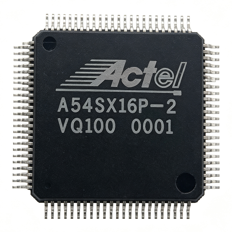
A54SX16-VQ100 - SX FPGA 16K Gates 100-TQFP | Microsemi
The Microsemi (Actel, now Microchip) A54SX16-VQ100 is an SX-family antifuse FPGA delivering 16,000 system gates with 924 logic cells, up to 240 MHz system performance, and 81 user I/O in a 100-pin TQFP (VQFP, 14x14 mm) package. It operates from dual supply rails of 3.0V to 3.6V and 4.75V to 5.25V and is fabricated on a 0.35 um CMOS process. An FPGA (Field Programmable Gate Array) is a semiconductor device containing a fabric of configurable logic blocks and programmable interconnects that the designer programs after manufacturing. Within the product hierarchy, the A54SX16 sits under FPGA -> programmable logic device -> digital integrated circuit. The SX family is unique among FPGAs because it uses Actel's antifuse technology: interconnects are one-time programmable at programming time, giving non-volatile, radiation-tolerant, low-power configuration without an external configuration PROM or boot sequence. Key differentiating features include the sea-of-modules architecture that yields gate utilization and speed close to mask ASICs, deterministic sub-nanosecond pin-to-pin delays, and instant-on operation at power-up because the configuration is hard-wired in silicon. The 0.35 um antifuse process also provides inherent protection against configuration readback, a security advantage over SRAM FPGAs. Architecturally, the SX family combines C-cells (combinational) and S-cells (sequential) in clusters, with the A54SX16 providing 924 cells of high-speed, flip-flop-rich logic. The device is programmed once using Actel/Microchip programming tools, after which the design is fixed for life - ideal for production systems where configuration integrity matters. Typical applications include industrial control, communications and networking glue logic, avionics and military subsystems, and ASIC prototyping where 16K gates suffice. Instant-on behavior also suits bridge and interface logic on boards that cannot wait for configuration. Design consideration: antifuse FPGAs are one-time programmable - any logic change requires a new device, so reserve spare I/O and validate the design thoroughly in simulation before committing to production programming. This page synthesizes verified distributor data, drop-in alternatives from the same SX family, and practical design notes not found in the manufacturer datasheet.
A54SX16-VQG100 - 24K Gate Antifuse FPGA, 81 I/O | Microsemi
The Microsemi (Microchip) A54SX16-VQG100 is a 24,000-gate antifuse FPGA from the SX family, offering 924 logic cells (1452 modules), 81 user I/O pins, and a 240 MHz system performance in a 100-pin VQFP/TQFP (14x14 mm) surface-mount package. It operates from dual supply rails of 3.0 V to 3.6 V and 4.75 V to 5.25 V and is fabricated on a 0.35 um CMOS process. An antifuse FPGA is a field-programmable gate array in which programmable interconnect points are permanently formed at programming time, unlike SRAM-based FPGAs that load configuration from an external memory at every power-up. Within the programmable logic hierarchy, the device sits between CPLDs and large SRAM FPGAs: its sea-of-modules architecture provides fine-grained logic modules that simplify design timing closure while delivering ASIC-like density and performance. Key features include the sea-of-modules architecture for reduced design time and power consumption, non-volatile antifuse interconnect that requires no configuration PROM and offers inherent design security, 240 MHz toggle performance suited to high-speed state machines and datapaths, and 81 configurable I/O for flexible board interfacing. The 3.3 V core and 5 V-tolerant-compatible dual-rail scheme ease integration into mixed-voltage industrial systems. Architecturally, the SX family combines C-cell and R-cell logic modules with an efficient routing fabric; the A54SX16 variant provides 1452 logic modules organized for predictable, low-skew routing. Because programming is one-time (OTP), configuration data cannot be read back, giving strong IP protection compared with SRAM FPGAs. Typical static power consumption is low relative to SRAM competitors of similar density, which benefits always-on industrial designs. Typical applications include glue logic consolidation and ASIC prototyping, industrial control and automation interfaces, aerospace and defense subsystems where non-volatile, secure configuration matters, communications line cards, and medical instrumentation requiring deterministic power-up behavior without an external boot device. A key design consideration is that antifuse devices are one-time programmable: design changes require a new physical part, so final RTL verification and timing sign-off must be complete before programming. The commercial (non-I) temperature grade should also be confirmed against the ambient range of the end system. This page synthesizes distributor inventory data, drop-in same-package alternatives from the same family, and practical design notes not found in the manufacturer datasheet, with pricing as of 2026-09-03.
A54SX16-VQG100I - 24K-Gate SX FPGA, 81 I/O, TQFP-100 | Microsemi
The Microsemi (Microchip) A54SX16-VQG100I is a 24,000-gate SX-family field programmable gate array (FPGA) with 924 logic cells, 81 configurable user I/O pins, and a 240 MHz system toggle rate, housed in a 100-pin VQFP/TQFP (14x14 mm) surface-mount package. It operates from dual supply rails of 3V to 3.6V and 4.75V to 5.25V and is rated for the industrial temperature range denoted by the I suffix. An FPGA (field programmable gate array) is a reprogrammable logic device that implements custom digital circuits through a configuration bitstream rather than fixed mask-programmed silicon. Within the programmable-logic hierarchy, the SX family sits among Actel/Microsemi antifuse FPGAs, one-time programmable devices prized for instant-on operation, low power, and high resistance to configuration upset compared with SRAM FPGAs. Key features include 24,000 system gates organized in a sea-of-modules architecture, 924 logic cells (about 1452 logic array blocks per distributor listings), support for 3.3V and 5V interfacing through dual voltage rails, and 81 flexible I/O pins. The antifuse interconnect yields deterministic, low-jitter routing and eliminates boot-up configuration time, a significant advantage over SRAM-based competitors such as the Xilinx XC4003A family. Technically, the SX family uses a 0.35 um CMOS process with a two-module (C-cell and R-cell) fabric that balances combinational and sequential logic density, enabling effective clock rates up to 240 MHz. The 5V-tolerant I/O structure supports legacy 5V bus systems alongside 3.3V core logic, which is why this family remains popular in defense, industrial, and telecommunications designs. Typical applications include glue-logic consolidation, bus bridging in industrial automation, address decoding and control in military/aerospace subsystems, and co-processing in telecommunications line cards. The industrial-grade VQG100I option suits -40C to +85C environments. Design consideration: because antifuse FPGAs are one-time programmable, verify the design fully in simulation (and ideally in a comparable device) before programming production units; a design change requires a new device. This page adds distributor-verified specifications, drop-in same-package alternatives, comparison tables, and practical design notes not consolidated in the manufacturer datasheet.
A54SX16A-1PQG208 - 24K Gate SX-A FPGA, 175 I/O | Microchip
The Microchip Technology A54SX16A-1PQG208 (originally Actel/Microsemi) is an SX-A family antifuse FPGA with 24,000 system gates, 1452 logic cells (CLBs), 175 user I/O, and a maximum toggle frequency of 263 MHz, housed in a 208-pin BFQFP (PQFP-208) package with 0.5 mm lead pitch. It operates from a 2.25V to 5.25V supply and supports a speed grade -1 with a 1.2 ns fast input setup time. An FPGA (Field-Programmable Gate Array) is a semiconductor device containing a fabric of programmable logic blocks and interconnects that designers configure after manufacturing. Within the FPGA hierarchy, the SX-A sits in the antifuse, one-time-programmable (OTP) category: unlike SRAM FPGAs, it retains its configuration permanently, requires no external configuration ROM, and is inherently more resistant to bit-flip and bitstream-readback attacks. Key features include the sea-of-modules architecture delivering ASIC-like performance, deterministic routing delays for timing closure, low static power typical of antifuse CMOS, and 175 programmable I/O supporting 5V-tolerant signaling. The combination of 24K gates and 263 MHz toggle rate suits glue logic consolidation, bus bridging, state machines, and high-speed control paths that would otherwise require multiple SPLDs or an ASIC. Technically, the device is built on a CMOS process with 1452 combination logic modules (CLBs) organized as sea-of-modules, achieving gate utilization levels near ASIC density. Antifuse programming provides permanent interconnect with negligible series resistance, contributing to speed and reliability. The -1 speed grade denotes the standard commercial timing grade of the SX-A family. Typical applications include industrial control and automation, telecommunications line cards, military/aerospace legacy systems, and embedded glue logic for microprocessor systems, where single-chip integration lowers BOM cost and board area. Design consideration: because the device is OTP, verify your logic thoroughly in simulation and, where practical, prototype on an in-system-programmable part of the family before committing the antifuse array. This page adds value beyond the manufacturer datasheet by consolidating distributor pricing tiers, pin-compatible same-package alternates, and drop-in replacement guidance for obsolescence-prone legacy designs.
A54SX16A-1PQG208I - 24K Gate Antifuse FPGA 208-PQFP | Microchip
The Microchip Technology (formerly Actel/Microsemi) A54SX16A-1PQG208I is a 24,000-system-gate antifuse FPGA from the SX-A family, offering 1,452 logic cells (CLBs), a maximum toggle-rate performance of approximately 263 MHz, 175 user I/Os, and a 208-pin Plastic Quad Flat Package (PQFP) in industrial temperature grade (-40C to +85C). An antifuse FPGA is a one-time-programmable (OTP) programmable logic device whose interconnect switches are formed by an antifuse element that permanently shorts when programmed. Within the programmable logic hierarchy, the SX-A sits in the FPGA category (field programmable gate array -> programmable logic device -> semiconductor), contrasting with SRAM-based FPGAs from Xilinx or Altera by requiring no configuration PROM, boot time, or configuration bitstream, which improves design security and power-on reliability. Key features include a sea-of-modules architecture built on a 0.25 um CMOS process, a 2.5V core supply for low power operation, and the -1 speed grade suitable for mid-range synchronous designs. The 175 user I/Os and 208-pin QFP footprint make the device well suited for glue logic consolidation, bus bridging, and control-plane functions that would otherwise require multiple discrete devices. Technical depth: the SX-A fabric combines C-cells (combinational) and R-cells (sequential) clustered in logic modules, delivering efficient flip-flop-heavy designs without the routing delays typical of larger SRAM FPGAs. The 1,452-cell array, per FindIC specifications (2007 datasheet publication), supports design entry in Verilog/VHDL via the Libero SoC toolchain. Typical applications include industrial automation control logic, avionics and defense systems requiring OTP security, telecommunications line-card glue logic, and obsolescence-driven redesigns replacing multiple 74-series devices. The industrial I grade extends operation to -40C to +85C for harsh environments. Design consideration: because the device is one-time programmable, fully verify the design in simulation before programming; there is no field re-work capability. This page synthesizes distributor pricing tiers, drop-in same-package alternatives, and practical design notes not consolidated in the manufacturer datasheet. Pricing shown is as of 2026-09-03.
A54SX16A-1PQG208M - 24K Gate Antifuse FPGA 208-PQFP | Microchip
The Microchip Technology A54SX16A-1PQG208M is an SX-A family antifuse FPGA (field-programmable gate array) offering 24,000 system gates, 175 user I/Os, and a -1 speed grade, housed in a 208-pin fine-pitch PQFP (BFQFP) surface-mount package. An FPGA is a programmable logic device that implements digital circuits by programming internal interconnects and logic modules. Within the programmable logic hierarchy, the A54SX16A belongs to the antifuse FPGA category: one-time programmable (OTP) devices in which each programmable interconnect is an amorphous silicon antifuse that permanently switches from high impedance to low resistance when programmed. Compared with SRAM-based FPGAs, antifuse FPGAs are non-volatile at power-up, resist readback and bitstream attacks, and consume far lower static power, making them a power management and security-friendly choice for glue logic integration. Key features include single-chip integration that replaces multiple discrete logic devices, support for 2.5 V, 3.3 V, and 5 V I/O signalling standards on 0.22 um / 0.25 um CMOS antifuse technology, and a low-power, high-performance fabric suitable for designs clocked at hundreds of megahertz (the SX16A family cell toggle rate is specified up to 263 MHz per distributor data). The -1 speed grade denotes the standard industrial speed bin of the SX-A family. The device architecture uses Actel's SX-A sea-of-modules fabric with clustered C-cells (combinational) and R-cells (sequential), connected through a segmented routing structure programmed by antifuse links. This yields deterministic, flip-flop-rich timing without configuration time at power-up. Typical applications include industrial control and automation glue logic, telecommunications and networking line-card functions, aerospace and defense designs requiring one-time-programmable security, and bridge/interface consolidation on microprocessor-based boards. Design consideration: because the antifuse is one-time programmable, prototype thoroughly in simulation (Libero/Microchip design flow) before programming production devices; there is no reprogramming fallback. This page adds distributor pricing context, same-brand drop-in alternatives, comparison tables, and design notes not found in the manufacturer datasheet. Pricing referenced below is as of 2026-09-03.
A54SX16A-1TQG100 - 16K Gate SX-A FPGA, 100-TQFP | Microchip
The Microchip Technology (Microsemi) A54SX16A-1TQG100 is an SX-A family antifuse FPGA offering approximately 16,000 typical gates (24,000 system gates) with 924 logic cells and 1,452 configurable logic blocks (CLBs), a maximum toggle frequency of 263 MHz, fabricated on a 0.25 um CMOS process at a 2.5V core supply, packaged in a 100-pin TQFP with 81 user I/Os. An FPGA (Field-Programmable Gate Array) is a semiconductor device containing configurable logic blocks and programmable interconnects that designers configure in the field to implement custom digital circuits. Within the programmable logic hierarchy, the A54SX16A sits in the antifuse one-time-programmable (OTP) FPGA category, positioned under programmable logic devices, distinct from SRAM-based FPGAs that require configuration storage. The Actel/Microsemi SX-A architecture uses a sea-of-modules structure delivering ASIC-like integration with low power and inherent security because the antifuse configuration cannot be read back. Key features include a 0.25 um antifuse CMOS process, 2.5V core operation with 2.25V to 2.75V supply tolerance, up to 263 MHz system performance in the -1 speed grade, 81 available user I/O, and single-chip integration of multiple glue-logic functions that reduces board cost and power. The SX-A family emphasizes performance, security, and low power at a low per-gate premium. Architecturally, each CLB provides combinatorial and sequential capability with fast local routing, and dedicated high-speed carry chains support arithmetic functions. The combinatorial CLB delay of the related A54SX16A-1TQG100A variant is specified with a maximum toggle of 278 MHz, indicating the family headroom across speed grades. Typical applications include industrial control and automation glue logic, communications and networking interface bridging, military/aerospace upgrade boards where OTP security is valued, and obsolescence-driven ASIC or CPLD consolidation designs. When designing with this device, plan for one-time programming: verify the design fully in simulation before programming, since antifuse parts cannot be reconfigured in-system. Power estimates should account for both static and dynamic terms using the manufacturer's tools. This page synthesizes distributor pricing (Mouser, DigiKey, Octopart), same-package drop-in alternatives, and design guidance not consolidated in the manufacturer datasheet.
A54SX16A-1TQG100I - 24K Gate FPGA 81 I/O TQFP-100 | Microchip
The Microchip Technology (formerly Actel/Microsemi) A54SX16A-1TQG100I is an SX-A family antifuse FPGA with 24,000 system gates (approximately 16,000 typical gates), 1452 configurable logic blocks (CLBs), 81 user I/Os, and a toggle rate of 263 MHz, built on a 0.25 um CMOS process with a 2.5V core supply in a 100-pin TQFP package. The industrial temperature grade (-40C to +85C) and lead-free, RoHS-compliant construction suit it for harsh-environment embedded systems. An FPGA (Field-Programmable Gate Array) is a semiconductor device containing a fabric of configurable logic blocks and programmable interconnects that designers configure to implement custom digital circuits. Within the programmable logic hierarchy, the SX-A sits in the one-time-programmable (OTP) antifuse FPGA category, positioned below flash-based and SRAM-based FPGAs but offering superior security and instant-on behavior. The sea-of-modules architecture of the SX family simplifies design migration and reduces power consumption relative to SRAM FPGAs. Key differentiating features include the antifuse fabric, which is non-volatile, requires no configuration PROM, and resists bit-stream extraction, making designs exceptionally hard to clone. The -1 speed grade supports clock rates up to 263 MHz toggle, and the 2.5V core delivers low static power compared with older 3.3V-generation FPGAs. The 100-lead TQFP (1.4 mm height) provides a cost-effective, hand-assembly-friendly surface-mount footprint. The SX-A architecture organizes logic into C-cells and R-cells with dedicated fast carry chains and a segmented routing matrix, enabling efficient datapath, state-machine, and glue-logic implementations. Because configuration is stored in antifuses, the device powers up instantly with no boot latency, and there is no external configuration flash to corrupt. Typical applications include industrial automation control, aerospace and defense subsystems, bridge/protocol conversion, bus interface bridging, and replacing multiple ASIC/MSI glue-logic chips in a low-cost single-chip solution. A key design consideration: antifuse FPGAs are one-time programmable, so prototype thoroughly in simulation; choose speed grade and package with future upgrades in mind since the same TQG100 footprint accommodates other SX-A family members. This page synthesizes distributor pricing, drop-in family alternatives, and practical design guidance not found in the manufacturer datasheet.
A54SX16A-1TQG100M - SX-A FPGA 24K Gates 81 I/O | Microchip
The Microchip Technology A54SX16A-1TQG100M is an SX-A family antifuse FPGA offering 24,000 system gates (16K gates, 924 cells), 81 user I/O, and toggle rates up to 263 MHz, fabricated on a 0.25 um process and housed in a 100-pin TQFP (LQFP-100) package with 0.5 mm pitch. It operates from a single 2.5 V supply with internal access times as fast as 1.2 ns. An FPGA (Field-Programmable Gate Array) is a semiconductor device containing a matrix of configurable logic blocks and programmable interconnects that the designer wires together after manufacturing. Within the programmable logic hierarchy, the SX-A sits in the one-time-programmable (OTP) antifuse FPGA category, positioned below SRAM-based FPGAs in reconfigurability but above them in security, power, and cost for many volume applications. Key features of the A54SX16A-1TQG100M include the low-cost antifuse architecture that is inherently non-volatile and resistant to bit-stream extraction, a 24K system-gate capacity suitable for glue logic consolidation, state machines, bus interfaces, and control functions, 81 flexible user I/O supporting multiple I/O standards, and typical toggle frequencies up to 263 MHz. The -1 speed grade balances performance with cost, and the M suffix denotes commercial temperature-range tray packaging. Technically, the SX-A family uses a 0.25 um antifuse process in which each programmable connection is a permanently-blown amorphous silicon link. This yields very low static power, no configuration PROM requirement, and no configuration time at power-up. Because the programming pattern is destroyed during programming, reverse engineering of the design is extremely difficult compared with SRAM FPGAs. Typical applications include industrial control and automation boards, telecommunications line cards, test and measurement instrumentation, defense upgrades of legacy designs, and single-chip integration of multiple discrete logic devices to reduce board area and BOM cost. Design consideration: antifuse FPGAs are one-time programmable, so design the RTL for finality and verify thoroughly in simulation before committing silicon; also note the 2.5 V core supply requires a dedicated regulator on mixed-voltage boards. This page synthesizes verified distributor data, drop-in family alternatives, design notes, and commercial information not consolidated in the manufacturer datasheet.
A54SX16A-1TQG144 - 24K-Gate Antifuse FPGA TQFP-144 | Microchip
The Microchip Technology (Microsemi/Actel) A54SX16A-1TQG144 is a 24,000-system-gate antifuse FPGA from the SX-A family with 1452 logic cells, 113 user I/O, and 263 MHz system performance, housed in a 144-pin TQFP (TQG144) surface-mount package. An antifuse FPGA is a type of field-programmable gate array in which programmable interconnect elements are one-time-programmable antifuse links. Unlike SRAM-based FPGAs, an antifuse device retains its configuration permanently, requires no external boot configuration memory, powers up instantly with its full function active, and is inherently resistant to configuration readback attacks. Within the programmable logic hierarchy, the A54SX16A sits in the mid-density segment of the SX-A family between the A54SX08A (8K gates) and A54SX32A (32K gates), and belongs to the broader category of one-time-programmable programmable logic devices. Key features of the A54SX16A-1TQG144 include a sea-of-modules architecture with a fine-grained C-cell/R-cell logic module structure that delivers deterministic timing, performance up to 263 MHz, and a wide core supply range of 2.25V to 5.25V. The device uses a 0.25 um CMOS process and offers roughly 16,000 typical usable gates for design implementation out of the 24,000 equivalent system gates. The SX-A architecture integrates combinational and sequential logic in dedicated modules, enabling designers to consolidate glue logic, bus interfaces, state machines, and control functions into a single low-cost chip. Because the programming antifuses are permanently set at the factory programming stage, the device offers high design security, low static power, and no configuration latency - key advantages over SRAM FPGAs for cost- and security-sensitive systems. Typical applications include industrial control and automation, communication and networking interface bridging, military and aerospace systems requiring secure one-time-programmable logic, and replacement of multiple discrete TTL/CMOS glue-logic devices on legacy board designs. A key design consideration is that the device is one-time-programmable: once programmed, the antifuse configuration cannot be changed, so design verification must be completed before committing to production programming. The TQFP-144 package with 1.4 mm height suits standard reflow assembly. This page synthesizes distributor pricing, speed-grade and package-family alternatives, and practical design notes not found in the manufacturer datasheet.
A54SX16A-1TQG144I - 16K Gate FPGA, TQFP-144 | Microchip
The Microchip Technology (Microsemi/Actel) A54SX16A-1TQG144I is a 16K-gate antifuse FPGA from the SX-A family, offering 924 logic cells, up to 263 MHz system performance, 113 user I/O, and a 2.5V core supply in a 144-pin TQFP package with industrial temperature rating (-40C to +85C). A field-programmable gate array (FPGA) is a semiconductor device containing a fabric of configurable logic blocks (CLBs) and programmable interconnects that engineers configure after manufacturing. Within the programmable logic hierarchy, FPGAs sit alongside CPLDs as logic-implementation devices, and the SX-A family uses antifuse (Actel) programming technology, which is one-time programmable but inherently non-volatile and more secure against bitstream readback than SRAM-based FPGAs. Key features of the A54SX16A-1TQG144I include 24,000 system gates on a 0.25 um CMOS process, pin-to-pin routing architecture with no dedicated routing delays, and a speed grade -1 with toggle rates to 263 MHz. The antifuse fabric provides flip-flops with fast setup times and low routing parasitics, delivering ASIC-like performance at FPGA economics. Supplying 113 user I/O in TQFP-144 makes it well suited for glue logic consolidation, bus interfacing, and state-machine replacement. The SX-A architecture integrates multiple discrete logic functions into a single low-cost chip, decreasing the performance premium while providing security and low power benefits, according to the Microchip product page. The 0.25 um technology and 2.5V core keep static power low, while the one-time-programmable antifuse removes the need for configuration ROM and eliminates configuration-time vulnerability. Typical applications include industrial control, aviation and military subsystems requiring configuration security, communications bridging, and legacy ASIC prototyping or low-volume production where masking costs are prohibitive. Designers should note that antifuse devices are one-time programmable: prototype thoroughly with the manufacturer design tools before committing, and verify I/O bank voltage compatibility with 3.3V peripheral logic. This page synthesizes distributor pricing, same-footprint alternatives, and practical design notes not found in the manufacturer datasheet, based on verified web data as of 2026-09-03.