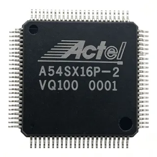
A54SX08-1VQG100I - 8K Gate SX FPGA 100-TQFP | Microsemi
MPN: A54SX08-1VQG100I ✗ End of Life| Qty | Unit Price | Extended |
|---|---|---|
| 1 | $0 | $0.00 |
| 10 | $0 | $0.00 |
| 100 | $0 | $0.00 |
| 500 | $0 | $0.00 |
| 1,000 | $0 | $0.00 |
A54SX08-1VQG100I Overview
An FPGA is a type of programmable logic device (PLD) that implements digital logic through configurable interconnect and logic blocks programmed by the designer, sitting above fixed-function ASICs in flexibility and below general-purpose processors in abstraction. Within the hierarchy of digital ICs, the Actel SX family belongs to the antifuse-based, one-time-programmable FPGA class, where configuration data is permanently stored in antifuse elements rather than SRAM cells.
Key features include the SX sea-of-modules architecture delivering ASIC-like performance, dual supply voltage operation (3.0V to 3.6V core region and 4.75V to 5.25V I/O region per the 3.3V/5V dual-supply scheme), and a 0.35um process technology. The one-time-programmable antifuse fabric makes the device non-volatile, secure against readback, and immune to configuration errors at power-up, which differentiates it from SRAM FPGAs such as the Xilinx XC4000 or Altera FLEX families.
Architecturally, the sea-of-modules structure provides high logic density and predictable timing: the 512 combinational and sequential cells connect through a routing fabric optimized for high fan-out, enabling the 280 MHz maximum toggle frequency. The 81 user I/O pins support the 5V-compatible signaling standards required in legacy industrial and avionics systems.
Typical applications include industrial control and automation, glue logic integration, high-reliability power-up-critical control logic, and communication backplane interfaces where one-time programmability and 5V I/O tolerance remain design requirements.
Design consideration: because antifuse programming is irreversible, verify the design fully in simulation and with the Actel/Microchip Libero design flow before programming production units.
This page synthesizes distributor availability, same-family drop-in package-compatible alternatives, and practical design notes not consolidated in the manufacturer datasheet.
Drop-in alternatives for A54SX08-1VQG100I — same package, pin-to-pin compatible. Different-package parts requiring PCB rework are excluded.
Variants in this series
Same-series models that are drop-in compatible with A54SX08-1VQG100I (same form factor and footprint) — differing in System Gates, Operating Temperature, Family, Speed Grade, Package.
Quick Comparison Tool — Select alternative parts for side-by-side comparison:
A54SX08-VQG100
✅ Drop-In✓ In Stock
$32.1 / Unit
View Datasheet →A54SX08-1VQ100
✅ Drop-In📋 Reference alternative (not in catalog)
A54SX16-VQG100I
✅ Drop-In✓ In Stock
Contact for price
View Datasheet →A54SX16-2VQ100
✅ Drop-In✓ In Stock
$29.75 / Unit
View Datasheet →A54SX16P-1VQG100I
✅ Drop-In✓ In Stock
$1870.24 / Unit
View Datasheet →A54SX16P-2VQG100I
✅ Drop-In✓ In Stock
$44 / Unit
View Datasheet →A54SX08-1VQG100I Maximum Ratings & Electrical Characteristics
| Logic Family / Series | Actel SX (A54SX08) |
| System Gates | 8K gates (12,000 usable gates per Microchip USA listing) |
| Logic Cells | 512 cells |
| Logic Elements | 768 |
| Maximum Toggle Frequency | 280 MHz |
| Process Technology | 0.35 um |
| Supply Voltage (Core Region) | 3 V to 3.6 V |
| Supply Voltage (I/O Region) | 4.75 V to 5.25 V |
| Supply Voltage Summary | 3.3 V / 5 V dual supply |
| User I/O | 81 |
| Package | 100-TQFP (VQFP, 14x14 mm) |
| Mounting Type | Surface Mount |
| Temperature Grade | Industrial (I suffix) |
| Programming Technology | Antifuse, one-time programmable (non-volatile) |
| Product Type | Field Programmable Gate Array (FPGA) |
A54SX08-1VQG100I 100-tqfp (vqfp, 14x14 mm) Pin Configuration Guide
Pin configuration for A54SX08-1VQG100I (100-tqfp (vqfp, 14x14 mm) package). This digital IC includes GPIO, communication interfaces (UART, SPI, I2C), and power pins. Refer to the manufacturer datasheet for alternate pin functions and configuration options. Essential for embedded system design and PCB layout.

No detailed pinout data available for A54SX08-1VQG100I.
Refer to the datasheet for full pin configuration.
Typical Applications
A54SX08-1VQG100I is suitable for 6 applications: Industrial Control and Automation, Glue Logic Integration, High-Reliability Power-Up-Critical Systems, Communication Backplanes and Line Cards, Legacy Design Sustainment and Obsolescence Bridge, Secure Configurable Logic.
Industrial Control and Automation
The A54SX08-1VQG100I fits industrial control because its 5V-compatible I/O signaling (4.75V-5.25V I/O rail) directly drives legacy TTL-level PLC inputs, sensor buses, and motor controller handshakes that 3.3V-only FPGAs cannot serve without level shifters. Its 512 cells and 280 MHz toggle rate host state machines, encoder interfaces, and interlock logic with ample margin, while the industrial temperature grade (-I suffix) covers factory-floor ambient extremes. The antifuse fabric powers up configured instantly with no external boot flash, eliminating the configuration-failure failure mode that stalls a production line. Placed between sensor banks and a main controller, the SX08 replaces dozens of 74-series glue devices, cutting board area and assembly cost while its one-time-programmable fabric prevents unauthorized logic modification on the plant floor.
Recommended
Glue Logic Integration
The A54SX08-1VQG100I is a classic glue-logic consolidator: 8K gates of antifuse fabric absorb address decoders, bus arbiters, wait-state generators, and interrupt controllers that would otherwise occupy a dozen or more SSI/MSI devices. Its dual 3.3V/5V supply means it bridges a 3.3V microprocessor to 5V peripheral buses natively, and the 81 user I/O provide enough pins for wide parallel buses. Because antifuse configuration is permanent, timing is fixed at programming, so bus setup/hold margins verified in simulation hold in every shipped unit - an advantage over SRAM FPGAs whose timing is identical but whose configuration can be corrupted. Designers typically reserve 20-30% of the 512 cells for late ECOs, using the Libero design flow to re-place logic without a board respin.
Recommended
High-Reliability Power-Up-Critical Systems
Systems that must be operational within microseconds of power application - safety interlocks, avionics discrete-logic replacements, and battery-management supervisory logic - benefit from the A54SX08-1VQG100I's antifuse technology. Unlike SRAM FPGAs that need a configuration device and boot interval (typically tens of milliseconds) during which outputs float or must be held, the SX08 is active as soon as the 3.3V/5V rails settle. The configuration cannot be read back or flipped by single-event upsets in the storage medium because there is no configuration memory to corrupt. The industrial-grade -I variant and Microsemi's aerospace heritage (the same fabric family underpins RTAX radiation-hardened devices) give reliability engineers a proven pedigree for these power-up-critical roles.
Recommended
Communication Backplanes and Line Cards
Telecom and industrial backplanes built on 5V TTL or 5V CMOS signaling levels use the A54SX08-1VQG100I for slot-address decoding, backplane arbitration, and LED/status multiplexing on line cards. The 280 MHz toggle capability covers timing budgets for fast backplane strobes, while 81 I/O accommodate wide 32-bit or 64-bit parallel data paths with control. The one-time-programmable fabric eliminates configuration storage on plug-in cards, simplifying hot-swap design because the device presents its configured function immediately on card insertion once supply rails reach 3.3V and 5V. Designers place 0.1 uF decoupling at each supply pin pair and hold the dual-rail sequencing within datasheet limits to avoid latch-up during card insertion transients.
Recommended
Legacy Design Sustainment and Obsolescence Bridge
Many legacy industrial, medical, and defense boards were designed around the Actel SX family in the late 1990s and 2000s; the A54SX08-1VQG100I remains a service part for those programs. Sustaining engineers use it to replace failed programmed devices (with the original programming file and a programming interface) or to rebuild spare-stock programs. When the SX08 itself becomes hard to source, the same-footprint A54SX16-VQG100I accepts the board-level footprint with a re-mapped Libero project, doubling available logic as headroom. Because the 54SX datasheet and Libero/Actel Designer toolchain remain available from Microchip, legacy netlists can still be rebuilt, programmed, and verified - extending system service life without a board respin.
Recommended
Secure Configurable Logic
Applications that must prevent logic reverse-engineering - proprietary industrial IP, secure dongles, and access-control sequencers - use the A54SX08-1VQG100I because antifuse configuration cannot be read back even by the programming tool after programming. There is no bitstream file to steal, unlike SRAM FPGAs whose configuration flash can be cloned from the boot device. The 8K gate capacity is sufficient for proprietary state machines, challenge-response logic paired with a host MCU, and key-scrambling glue around communication interfaces. Industrial-grade temperature qualification keeps the device dependable in uncontrolled environments, and the permanent programming means tamper attempts require physical decapping rather than a bus-level attack, raising the attack cost substantially.
Recommended
Recommended Products Summary
Engineering reference data for A54SX08-1VQG100I — comparison, design guidance, and compliance information.
Selection Guide
Comparison with Alternatives
| Parameter | This Product | A54SX08-VQG100 | A54SX08-1VQ100 | A54SX16-VQG100I | A54SX16-2VQ100 | A54SX16P-1VQG100I |
|---|---|---|---|---|---|---|
| Package | 100-TQFP (VQFP, 14x14 mm) | 100-TQFP (VQFP, 14x14 mm) - same | 100-VQFP (14x14 mm) - same | 100-TQFP (VQFP, 14x14 mm) - same | 100-VQFP (14x14 mm) - same | 100-VQFP (14x14 mm) - same |
| Brand | Microsemi | Microsemi | Microsemi | Microsemi | Microsemi | Microsemi |
| System Gates | 8K | 8K | 8K | 16K | 16K | 16K |
| Temperature Grade | Industrial (-I) | Commercial | Industrial | Industrial (-I) | Commercial | Industrial (-I) |
| Speed Grade | -1 | Standard | -1 | Standard | -2 (faster) | -1 |
| Programming Technology | Antifuse, one-time programmable | Antifuse, one-time programmable | Antifuse, one-time programmable | Antifuse, one-time programmable | Antifuse, one-time programmable | Antifuse, one-time programmable |
Key Differentiators
- Industrial temperature grade in a scarce package option (vs A54SX08-VQG100)
- Same-footprint capacity upgrade available (vs A54SX16-VQG100I)
- Faster speed grade option in same package (vs A54SX16-2VQ100)
Design Notes
The A54SX08-1VQG100I requires two supply rails: 3.0-3.6 V (core region) and 4.75-5.25 V (I/O region). Decouple each rail with 0.1 uF ceramic capacitors at every VCC/VCCI pin pair plus one bulk 10 uF capacitor per rail. Pay attention to power-up sequencing per the 54SX datasheet supply-requirements section - applying the 5V I/O rail long before the 3.3V core rail can forward-bias I/O structures. Estimated: at typical SX08 static current levels the device dissipates well under 0.5 W, so no heatsink is needed; verify with your design's I/O switching activity.
Antifuse FPGAs are one-time programmable - a misprogrammed device cannot be erased and reused. Complete full post-layout timing simulation and a hardware pilot run on a development socket before programming production quantities. Reserve 20-30% of the 512 cells and keep uncommitted I/O assigned in your Libero/Designer project so that late ECOs do not force a board respin. Also confirm the exact order-code suffix (temperature and speed grade) when purchasing, since the A54SX08 family spans multiple grades in identical 100-pin packages.
The 100-pin TQFP (14x14 mm, 0.5 mm lead pitch) requires fine-pitch SMD land patterns per the manufacturer package drawing; use a no-clean flux process and inspect with 10x magnification or X-ray for solder bridging on the 0.5 mm pitch leads. Route the programming pins (including VPP) with short traces to a programming header if in-system programming is planned. Keep 5V I/O traces away from the 3.3V core traces by at least 2x trace width to limit coupling, and provide a solid ground plane under the die center for signal return.
Compliance Information
Compliance data was not present in the retrieved web data as of 2026-09-03; verify RoHS/REACH status on the Microchip product page before export-controlled or EU-bound designs.