Logic ICs
Products (88)
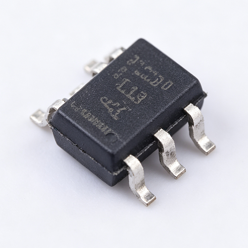
SN74AHC1G08-Q1 - Automotive 2-Input AND Gate SC-70-5 | TI
The Texas Instruments SN74AHC1G08-Q1 is an automotive-qualified single 2-input positive-AND gate that performs the Boolean function Y = A AND B in positive logic. Operating from a 2V to 5.5V supply, the device delivers a maximum propagation delay of 9 ns at 5V and comes in a 5-pin SC-70 (DCK) surface-mount package. A single-gate logic IC integrates exactly one logic function - here an AND gate - in a tiny footprint, unlike traditional quad-gate devices such as the 74HC08. Single-gate devices sit within the broader CMOS logic IC family, under combinational logic, and are widely used for glue logic, signal gating, and enable generation in modern PCBs where board space is at a premium. Key features include the AHC family's balanced CMOS architecture for low static power consumption, a wide 2V to 5.5V operating range supporting both 3.3V and 5V systems, and latch-up performance exceeding 250 mA per JESD 17. ESD protection exceeds 2000-V Human-Body Model, 200-V Machine Model, and 1000-V Charged-Device Model per TI datasheet. The -Q1 suffix denotes AEC-Q100 qualification for automotive applications. The AHC technology provides TTL-compatible CMOS outputs with balanced drive and fast switching, while the unbuffered single-stage design keeps propagation delay tight and predictable across the operating range. Typical applications include automotive body electronics and cluster gating, industrial PLC I/O conditioning, and general-purpose enable/signal gating in mixed 3.3V/5V systems. Design tip: keep unused input pins tied to VCC or GND, and place a 0.1uF decoupling capacitor close to the VCC pin to ensure clean switching edges and minimize ground bounce in automotive noise environments.

SN74AHC3G99-Q1 - Triple Configurable Logic Gate AEC-Q100 | TI
The Texas Instruments SN74AHC3G99-Q1 is an automotive-grade triple ultra-configurable multiple-function gate containing three independent configurable logic gates, each with four inputs and a 3-state output, implementing the Boolean function Y = (A • C + B • C) ⊕ D. It operates over a 2V to 5.5V supply range, making it compatible with 3.3V and 5V logic systems, and is qualified per AEC-Q100 for automotive environments. Configurable logic gates are digital ICs that let a single device implement multiple Boolean functions - MUX, AND, OR, NAND, NOR, XOR, XNOR - depending on input connections. They belong to the standard logic gate family within digital ICs, the fundamental building blocks of digital electronics. Integrating three such gates in one package saves board space and simplifies inventory versus discrete gates. Key features include Schmitt-trigger inputs on every pin, which eliminate erroneous outputs caused by slow-edged or noisy input signals - critical in electrically harsh automotive systems. The 3-state outputs place pins in a high-impedance state, enabling bus sharing. Per the TI datasheet, the device drives load capacitance up to 50pF while meeting all datasheet specifications, with a typical propagation delay of 7.5ns at 5V for high-speed operation. Technically, the device is built on TI AHC (Advanced High-Speed CMOS) technology, balancing speed with low static power consumption. Input hysteresis improves noise immunity and permits slow input transitions without false triggering, while output-enable control supports bus-oriented architectures. Typical applications include automotive body control modules, infotainment systems, and industrial automation where multiple logic functions are required in a compact footprint. It also suits signal conditioning in mixed-voltage systems. Design tip: keep total output load capacitance at or below 50pF to preserve full datasheet timing, and place a 0.1uF decoupling capacitor close to VCC to suppress supply noise.
SN74AHC9541-Q1 - AEC-Q100 Octal Buffer, Schmitt | TI
The Texas Instruments SN74AHC9541-Q1 is an automotive-grade octal buffer and line driver featuring Schmitt-trigger inputs and 3-state outputs, qualified to AEC-Q100 for harsh automotive environments. It operates from a 2V to 5.5V supply, supports -40C to +125C ambient temperatures, and is offered in a wettable-flank QFN (VSSOP-20) package that enables reliable solder-joint inspection. An octal buffer is a digital logic IC providing eight independent buffering channels that isolate, amplify, and restore digital signals. Buffers sit within the standard logic family hierarchy (CMOS logic > buffers/line drivers > single gates), preventing loading effects on driving circuits and regenerating weak or degraded signals across PCB traces, cables, and backplanes. Schmitt-trigger inputs add hysteresis, converting slow or noisy input edges into clean, fast output transitions. Key features include the wide 2V to 5.5V operating range compatible with 3.3V and 5V logic systems, dual active-low output enables (OE1 and OE2) that must both be low to activate all eight outputs, and AEC-Q100 automotive qualification. According to the TI datasheet, the device drives loads with total capacitance up to 50pF while meeting all datasheet specifications; larger loads may be applied but exceeding 50pF is not recommended. Fabricated in AHC-series CMOS technology, the device delivers low static power consumption, high speed, and balanced drive. The wettable-flank QFN package improves wetting of the package edge during soldering and enables automated optical inspection (AOI), a key automotive quality requirement. Typical applications include automotive body control modules, infotainment systems, ADAS signal buffering, and industrial interfaces where slow or noisy signals must be conditioned or held during controller reset. Design tip: keep per-output capacitive loading at or below 50pF, place 0.1uF decoupling capacitors close to VCC, and tie unused inputs to VCC or GND - never leave CMOS inputs floating.

SN74AHCT3G99-Q1 - Triple Configurable Gate | TI | Automotive
The SN74AHCT3G99-Q1 is an automotive-grade triple ultra-configurable multiple-function gate from Texas Instruments, containing three independent configurable logic gates with 3-state outputs in a 20-pin TSSOP (PW) package. Each gate has four inputs and implements the Boolean function Y = (A • /C + B • C) ⊕ D, which users can configure for functions such as MUX, AND, OR, NAND, NOR, XOR, and XNOR by appropriately strapping the inputs. A configurable multiple-function gate is a logic IC that can be wired to perform different Boolean operations, allowing one device to replace several fixed-function gates and reducing component count and board space. In the digital logic hierarchy it belongs to the configurable standard logic family, a subset of logic ICs within the broader category of integrated circuits. The SN74AHCT3G99-Q1 is part of the AHCT family - high-speed silicon-gate CMOS with TTL-compatible inputs - bridging CMOS efficiency and TTL logic levels. Key features include Schmitt-trigger inputs on all pins, which eliminate erroneous outputs caused by slow-edged or noisy input signals, and 3-state outputs that permit bus-oriented applications with high-impedance isolation. The supply range is 4.5V to 5.5V for full datasheet performance, and the device is AEC-Q100 qualified with an operating temperature range of -40C to +125C for harsh automotive environments. TI specifies the device can drive a total load capacitance of up to 50pF while meeting all datasheet specifications; larger loads are possible but not recommended. Technically, the device is fabricated in advanced CMOS, providing low static power consumption with TTL-level input thresholds. Propagation delay is [DATA_NEEDED: propagation delay] and output drive current is [DATA_NEEDED: output drive current]. The 3-state outputs are controlled via output-enable (OE) inputs, and Schmitt-trigger hysteresis of [DATA_NEEDED: hysteresis voltage] ensures clean switching on slow edges. Typical applications include automotive body control modules, infotainment units, and industrial control systems needing flexible glue logic, signal routing, or level-compatible logic functions. AEC-Q100 qualification guarantees reliability under automotive temperature, vibration, and ESD stress. When designing with this device, place decoupling capacitors close to the supply pins, keep output load capacitance at or below 50pF, and tie every OE input to a defined logic level to avoid floating bus contention.
SN74AHCT7541-Q1 - Automotive Octal Buffer, Open-Drain | TI
The SN74AHCT7541-Q1 from Texas Instruments is an automotive-grade octal buffer with open-drain outputs, operating from a 4.5V to 5.5V supply in a 20-pin TSSOP (PW) package. It contains eight non-inverting buffers with active-low output enable pins (OE1 and OE2); both enables must be low for the outputs to be active. When enabled, outputs actively drive low or present a high-impedance state; when disabled, outputs are high impedance. The device is AEC-Q100 qualified for a +125C ambient grade with HBM ESD protection. An octal buffer is a digital IC providing eight independent buffer channels used to increase fan-out, drive capacitive loads, or interface between voltage domains. With open-drain outputs, the device sinks current to ground when active, which makes it ideal for driving LEDs and implementing wired-OR logic. Schmitt-trigger inputs add hysteresis for superior noise immunity in automotive and industrial environments. Key features include the 4.5V to 5.5V supply range, open-drain outputs suited to external pull-up voltages above VCC, and inputs that tolerate slow edge rates thanks to Schmitt-trigger hysteresis. Per the TI datasheet, the device drives loads with total capacitance up to 50pF while meeting all datasheet specifications; larger capacitive loads are possible but not recommended. Output low-level current capability is defined by the VOL/IO characteristics in the Electrical Characteristics table. Technically, the device uses Advanced High-Speed CMOS TTL-compatible (AHCT) technology, balancing speed and power. External pull-up resistors define the output high level, a critical design consideration for wired-OR buses and mixed-voltage interfacing. The -40C to +125C operating range suits under-hood and body-electronics environments. Typical applications include automotive dashboard indicator LED drivers, level shifting between 5V and higher-voltage domains, wired-OR interrupt lines, and industrial control I/O requiring high noise immunity. Design tip: size pull-up resistors for the desired high level and sink current, tie OE1/OE2 appropriately, and place a 0.1uF decoupling capacitor close to the VCC pin.

SN74ALS253 - Dual 4:1 Mux 3-State ALS TTL | Texas Instruments
The Texas Instruments SN74ALS253 is a dual 1-of-4 data selector/multiplexer with 3-state outputs, fabricated in Advanced Low-Power Schottky (ALS) TTL technology and offered in 16-pin packages including Plastic DIP (N), Small-Outline (D), ceramic chip carrier (FK), and ceramic J packages. Each half multiplexes one of four data inputs to a single 3-state output under two common select lines, with separate active-low output-control (OE) inputs per section. A multiplexer is a combinational logic device that selects one of several input signals and forwards it to a single output, serving as a fundamental building block in the digital logic hierarchy between basic gates and larger bus-oriented logic systems. The 74-family lineage spans standard TTL (74), Schottky (74S), Low-Power Schottky (74LS), Advanced Low-Power Schottky (74ALS), and CMOS variants such as 74HC and 74HCT. Key features include full binary decoding with internal inverters and drivers feeding AND-OR gate structures, 3-state outputs that directly drive bus-organized data lines, and the ALS speed-power advantage over LS parts: faster propagation with substantially lower supply current. It is the 3-state version of the ALS153 and SN74AS153, permitting multiplexing from n lines to one line and parallel-to-serial conversion. Typical applications include bus-organized system data selection, parallel-to-serial data conversion, n-line to 1-line multiplexing in industrial controllers, and legacy TTL system maintenance and repair where ALS-era timing margins must be preserved. Design consideration: as an older bipolar TTL family, the SN74ALS253 requires a regulated 5V supply and presents TTL-level input thresholds; when integrating into mixed-voltage modern designs, verify logic-level compatibility or consider CMOS substitutes such as 74HC253 with attention to timing.
SN74ALVCH162373 - 16-Bit 3-State Transparent Latch | TI
The Texas Instruments SN74ALVCH162373 is a 16-bit transparent D-type latch with 3-state outputs, part of the ALVCH low-voltage CMOS Widebus family. It operates from a 2.3V to 3.6V supply and can function as two independent 8-bit latches or one 16-bit latch, controlled by latch-enable (LE) and output-enable (OE) inputs. When LE is high, the Q outputs follow the D inputs; when LE is low, the outputs hold the last data. A transparent latch is a sequential logic component that passes input data to outputs while enabled and stores the last value when disabled. It sits in the hierarchy: transparent latch -> D-type latch -> latch -> sequential logic -> digital logic IC, and is a fundamental building block for data storage, synchronization, and bus interfacing in digital systems. Key features include bus-hold circuitry on data inputs, which eliminates external pull-up or pull-down resistors; equivalent 26-ohm series resistors on output ports, removing the need for external line-termination resistors; and latch-up performance exceeding 250 mA per JESD 17, plus ESD protection. The 3-state outputs allow multiple devices to share a common bus, and the Ioff feature supports partial-power-down operation without backflow current. Technically, the device uses advanced low-voltage CMOS technology, providing high speed with low static power consumption. Propagation delay is typically around 4.1 ns at 3.3V, with +/-12 mA output drive at 3.3V, suitable for moderate capacitive loads. It is characterized for operation from -40C to +85C in industrial environments. Packages include 48-SSOP (DL), 48-TSSOP (DGG/GR), and 56-BGA MicroStar Junior (KR). Typical applications per the TI datasheet include buffer registers, I/O ports, bidirectional bus drivers, and working registers in memory interfaces, data acquisition systems, and general-purpose logic. Design tip: place 0.1uF decoupling capacitors close to each VCC pin, and verify timing margins since the integrated 26-ohm output resistors slightly slow edge rates at high frequencies.

SN74AUC2G34 - Dual Buffer Gate 0.8-2.7V | Texas Instruments
The Texas Instruments SN74AUC2G34 is a dual non-inverting buffer gate from the AUC (Advanced Ultra-CMOS) logic family, performing the Boolean function Y = A in positive logic. It operates from a 0.8 V to 2.7 V supply, specifically optimized for 1.65 V to 1.95 V operation, and is offered in the 6-pin SOT-23 (DBV) and SC70/SOT-563 (DCK) surface-mount packages for space-constrained portable designs. A buffer gate is a digital logic IC that passes its input to the output without inversion while regenerating drive strength and providing signal isolation. Within the logic-IC hierarchy (buffer gate -> logic IC -> digital integrated circuit), buffers are used to drive capacitive loads, isolate buses, and restore weak or degraded signal edges in low-voltage digital systems. Key features include sub-1-V operability, 3.6-V I/O tolerance for mixed-mode signal operation, and Ioff support for partial-power-down architectures. According to the TI datasheet (Rev. B), maximum propagation delay is 1.8 ns at 1.8 V with a +/-8-mA output drive at 1.8 V and low dynamic power consumption. NanoFree package technology in the smallest variants uses the die itself as the package. Architecturally, the device uses advanced ultra-low-voltage CMOS technology for high noise immunity and low static current. Ioff circuitry disables outputs and blocks damaging backflow current when VCC is removed while inputs remain driven - critical for multi-rail systems with flexible power sequencing. Typical applications include signal buffering in smartphones and tablets, clock distribution, 1.8 V to 3.3 V domain-tolerant interfacing, and bus isolation in industrial and consumer electronics. Design tip: place a 0.1 uF decoupling capacitor close to VCC and ensure input signals never exceed the absolute maximum rating of 4.6 V.
SN74AUP1T34-Q1 - 1-Bit Dual-Supply Level Translator | Texas Instruments
The Texas Instruments SN74AUP1T34-Q1 is a 1-bit unidirectional, noninverting voltage-level translator that operates from two separate configurable power-supply rails (VCCA and VCCB). It translates logic signals from A to B and comes in a 5-pin SC-70 (DCK) package qualified to AEC-Q100 for automotive applications, operating from -40C to +125C. A voltage-level translator is a logic IC that converts signals between two different voltage domains, allowing a 1.8V microcontroller to safely drive a 3.3V peripheral or vice versa. Translators sit within the broader logic IC family, alongside buffers, gates, and bus switches, and are essential wherever mixed-voltage systems interface. Key features include dual-supply operation enabling level translation in either direction (up or down), the AUP (Advanced Ultra-low Power) process family for very low dynamic power consumption, and push-pull output structure that removes the need for pull-up resistors required by open-drain translators. Per the TI datasheet, pin A is referenced to VCCA and receives the signal to be translated. The device belongs to TI's AUP1T single-gate translator family, which combines tiny single-gate packaging with wide supply flexibility, making it suitable for space-constrained automotive modules. The noninverting buffer topology preserves signal polarity with minimal propagation delay. Typical applications include automotive body electronics and lighting modules, level-shifting between 1.8V MCUs and 3.3V CAN or LIN transceivers, interfacing low-voltage sensors to higher-voltage logic, and general-purpose single-bit signal conversion in infotainment and cluster designs. Design consideration: ensure both supply rails are within the datasheet-recommended ranges and observe power-up sequencing guidance in the datasheet to avoid undefined outputs during startup. Because this is a unidirectional translator, the signal must always flow from pin A to pin Y/B.
SN74AUP1T34DSFR - 1-Bit Level Translator X2SON-6 | Texas Instruments
The Texas Instruments SN74AUP1T34DSFR is a 1-bit non-inverting unidirectional voltage-level translator in a 6-pin X2SON (DSF) package measuring 1x1 mm, operating over -40C to +85C. It uses two separate configurable power-supply rails, allowing logic signals to be translated between voltage domains such as 1.8V-to-3.3V or 1.2V-to-2.5V systems. A voltage-level translator is a member of the logic IC family (buffers, drivers, level translators within the broader category of digital integrated circuits) that converts digital signals from one logic-voltage domain to another. As process nodes shrink, modern MCUs, FPGAs, and sensors run on cores as low as 0.8V to 1.8V, while legacy peripherals, LEDs, and actuators still operate at 2.5V, 3.3V, or 5.5V. A dual-rail translator such as the SN74AUP1T34 bridges these domains safely, protecting input structures and guaranteeing valid logic levels on both sides. Key features include the AUP (Advanced Ultra-low Power) process family, known for the lowest dynamic power consumption in the TI small-signal logic portfolio, a push-pull (totem-pole) output that eliminates the need for an external pull-up resistor, and a non-inverting buffer function that preserves signal polarity. The tiny 1x1 mm X2SON footprint suits densely packed wearable, mobile, and IoT boards where every square millimeter counts. Technically, the device is a single-channel translator with the A port referenced to VCCA and the B port referenced to VCCB. Because the output is push-pull rather than open-drain, it delivers symmetric rise and fall times with lower static current than open-drain solutions. The Ultra-low-power AUP technology keeps dynamic power low during signal transitions, extending battery life in portable designs. Typical applications include GPIO level translation between microcontrollers and peripherals, I2C-adjacent and UART/SPI signal translation in portable consumer electronics, and interfacing low-voltage sensor outputs to higher-voltage logic in battery-powered IoT nodes. Design tip: power up VCCA before or together with VCCB and keep both rails within the datasheet-recommended operating window; decouple each rail with a 100 nF ceramic capacitor placed as close as possible to the pins to suppress transients on this compact package. This page synthesizes distributor pricing, drop-in alternatives, pinout detail, and practical design notes not found in a single manufacturer datasheet.
SN74AUP1T34QDCKRQ1 - AEC-Q100 1-Bit Level Translator | TI
The Texas Instruments SN74AUP1T34QDCKRQ1 is an AEC-Q100 qualified 1-bit unidirectional non-inverting voltage-level translator with dual configurable power-supply rails supporting VCCA and VCCB from 0.9V to 3.6V each, housed in a 5-pin SC-70 (DCK) surface-mount package rated from -40C to +125C. A voltage-level translator (also called a level shifter) is a logic IC that interfaces digital signals between circuits operating at different supply voltages, for example connecting a 1.8V microcontroller output to a 3.3V peripheral input. Level translators sit within the broader logic IC family (buffers, translators, transceivers) and are essential wherever mixed-voltage domains coexist, which is nearly every modern embedded system. Key features include two independent supply rails (VCCA and VCCB) that can each be set anywhere from 0.9V to 3.6V, allowing any-to-any translation between common logic levels such as 1.2V, 1.5V, 1.8V, 2.5V and 3.3V. The push-pull (non-inverting) output drives the signal actively in both directions, eliminating the need for external pull-up resistors required by open-drain solutions. The AUP (Advanced Ultra-low-Power) silicon technology delivers low dynamic power consumption, making the device attractive for battery-powered automotive and portable designs. Architecturally, pin A is referenced to VCCA and receives the input signal, while pin B is referenced to VCCB and transmits the level-shifted output. Because both supplies support the same 0.9V to 3.6V range, the translator is direction-agnostic in voltage terms: it can translate low-to-high or high-to-low. TI controls the data sheet SN74AUP1T34-Q1, and the -Q1 suffix denotes AEC-Q100 automotive qualification including extended -40C to +125C operation. Typical applications include automotive body electronics and ADAS sensor interfaces, I2C/SPI/UART signal translation between mixed-voltage ICs, GPIO level conversion in battery-powered portable equipment, and general-purpose 1-bit buffering in industrial control modules. Design consideration: both VCCA and VCCB must be decoupled with 0.1uF ceramic capacitors placed close to pins 4 and 5, and the unused input should never be left floating since the AUP family inputs must be tied high or low. This page adds value beyond the TI datasheet by synthesizing distributor pricing as of 2026-09-04, drop-in alternative analysis, and practical layout notes in one place.

SN74AVC4T234 - 4-Bit Dual-Supply Level Translator | TI
The SN74AVC4T234 is a 4-bit, dual-supply noninverting voltage level translation device from Texas Instruments. It is designed to facilitate asynchronous communication between B-port inputs and A-port outputs, with each port referenced to its own supply rail (VCCB and VCCA). The device operates across a wide VCC range of 0.9 V to 3.6 V, making it suitable for low-power, battery-powered portable applications where both static and dynamic power consumption must be minimized. A voltage level translator, also known as a level shifter, is a type of logic IC that allows digital signals to be transferred between circuits operating at different voltage levels. It is essential in mixed-voltage systems, such as interfacing a 1.8V microcontroller with a 3.3V peripheral. The SN74AVC4T234 belongs to the AVC family of advanced very-low-voltage CMOS logic, which is optimized for high-speed operation with minimal power consumption. Key features of the SN74AVC4T234 include its dual-supply configuration, which provides independent power rails for each port, ensuring proper voltage translation without signal distortion. The device maintains excellent signal integrity across the entire VCC range, and its low static and dynamic power consumption extends battery life in portable devices. The noninverting architecture preserves signal polarity, simplifying system design. Technically, the SN74AVC4T234 uses a configurable voltage translation scheme that automatically adjusts output drive strength based on the supply voltage. This ensures reliable operation even with varying supply levels. The device is available in a small package, making it ideal for space-constrained applications. Its propagation delay is minimal, supporting high-speed data transfer. Typical applications include interfacing between different voltage domains in smartphones, tablets, and other portable electronics, as well as in industrial control systems where sensors and microcontrollers operate at different voltages. The device is also used in networking equipment and data communication systems. When designing with the SN74AVC4T234, ensure that both VCCA and VCCB are powered and within the specified range. Proper decoupling capacitors should be placed near the supply pins to maintain stable operation. The device supports bidirectional level translation, but the direction is controlled by the DIR pin, which must be set correctly for the desired data flow.

SN74AVC4T245PWR - 4-Bit Dual-Supply Level Shifter | TI
The Texas Instruments SN74AVC4T245PWR is a 4-bit dual-supply bus transceiver with configurable voltage translation and 3-state outputs, supplied in a 16-pin TSSOP (PW) package. It operates from two independent supply rails, VCCA and VCCB, each ranging from 0.8V to 3.6V, enabling bidirectional level shifting between mixed voltage domains such as 1.2V, 1.5V, 1.8V, 2.5V, and 3.3V. A bus transceiver is a digital integrated circuit that transfers data bidirectionally between two buses, using direction-control and output-enable inputs plus 3-state outputs so multiple devices can share a common bus. The SN74AVC4T245 belongs to the voltage translator (level shifter) family within the broader logic IC and interface IC hierarchy, and it is essential in mixed-voltage systems where MCUs, FPGAs, sensors, and memory operate at different logic levels. Key features include configurable voltage translation on both ports, control inputs (1DIR, 2DIR, 1OE, 2OE) referenced to VCCA for simplified control logic, and Ioff partial-power-down circuitry that disables outputs and prevents damaging backflow current when either rail is at GND. A VCC isolation feature places all I/O in high-impedance if either supply is absent. Technically, the device supports asynchronous communication between two data buses at data rates up to 380 Mbps with a typical propagation delay around 2.5 ns, suiting high-speed SPI, parallel bus, and GPIO interfaces. The TSSOP-16 package has a 4.4mm body width and 0.65mm pin pitch for space-constrained PCBs. Typical applications include level shifting for SPI, UART, I2C-adjacent GPIO expansion, and FPGA or ASIC interconnects in industrial control, portable battery-powered electronics, and automotive modules where multiple voltage domains coexist. Design tip: keep the DIR and OE pins driven from VCCA-domain logic and place 0.1uF decoupling capacitors close to both VCCA and VCCB pins; avoid bus contention by sequencing direction changes with a brief high-impedance interval.

SN74BCT574 - Octal D-Type Flip-Flop 3-State | Texas Instruments
The Texas Instruments SN74BCT574 is an octal D-type edge-triggered flip-flop with 3-state outputs, built on a state-of-the-art BiCMOS process and designed to drive highly capacitive or relatively low-impedance loads in high-speed bus-oriented systems. It operates from a 4.5 V to 5.5 V supply and is offered in DB (SSOP), DW (SOIC), N (PDIP), and NS (SOP) packages. An octal D-type flip-flop is a digital logic register that stores eight bits of data, capturing the logic level present on each D input at the rising edge of a common clock and presenting it on the corresponding Q outputs. In the broader logic-IC hierarchy, it belongs to the flip-flop and register family of sequential logic, a core building block of microprocessor bus interfaces. Its 3-state outputs can be disabled via an active-low output-enable (OE) pin, allowing multiple devices to share a common data bus without contention. Key features include the BiCMOS design that significantly reduces ICCZ (high-impedance supply current), full parallel access for loading all eight bits on one clock edge, and strong bipolar output drive for heavy capacitive bus loads. According to TI datasheet SCBS074C, the edge-triggered architecture guarantees that data is captured only on the rising clock edge, giving predictable setup and hold behavior in synchronous systems. Technical depth: the BCT (BiCMOS) technology combines TTL-compatible input thresholds with bipolar totem-pole output stages, delivering low dynamic supply current at high clock frequencies and high output current capability, making it superior to pure CMOS ABT/ACT predecessors for heavily loaded 5 V buses. Typical applications include buffer registers, I/O ports, bidirectional bus drivers, working registers in microprocessor systems, memory address/data latching, industrial control, and communication interfaces where reliable latching plus high bus drive are required. Design tip: control OE properly to avoid bus contention (OE low enables outputs, high forces high-Z), decouple VCC close to the pins with 0.1 uF ceramic capacitors, and drive the clock with a clean edge to avoid metastability.

SN74CBT3245ADWR - Octal FET Bus Switch 5V SOIC-20 | TI
The Texas Instruments SN74CBT3245ADWR is an octal FET bus switch providing eight bits of high-speed TTL-compatible bus switching in a 20-pin SOIC (DW) package with the standard 245-type pinout. Operating from a 4.5V to 5.5V supply, the device is organized as a single 8-bit switch with one output enable (OE) control input; when OE is low, the switch connects the two 8-bit ports bidirectionally. A FET bus switch is a type of analog switch that uses N-channel MOSFET pass transistors to connect or disconnect signal paths between two ports. Within the signal-routing hierarchy, bus switches sit between logic buffers and analog multiplexers: unlike buffers they add negligible propagation delay, and unlike analog MUXes they are optimized for high-bandwidth digital bus isolation. The SN74CBT3245A belongs to the CBT (CrossBar Technology) family, optimized for low on-state capacitance and high bandwidth. Key features include a low on-state resistance of typically 5 ohms, propagation delay of less than 250 ps, and near-zero added jitter because signals pass through an analog FET path rather than a buffered logic stage. The switch supports bidirectional data flow and 5-V level handling, suited to signal switching rather than power delivery. Technically, the device is fabricated in a CMOS process achieving low static power consumption. The internal FET switch presents a low-capacitance, low-resistance path that minimizes signal distortion, and the 245-type pinout matches industry-standard octal transceiver footprints across SOIC, SSOP, TSSOP, and TVSOP package options. Typical applications include bus isolation in microprocessor systems, hot-swap and power-down isolation on backplanes, memory bus switching, and signal routing in networking and telecommunications equipment where high-speed data buses must be connected or isolated under logic control. A key design consideration: control the OE pin properly to avoid bus contention, and note this part is EOL per TI.com - plan the drop-in alternatives listed on this page for new designs.
SN74CBTLV3257PWR - 4-Bit 2:1 FET Mux 5Ω | TI
The Texas Instruments SN74CBTLV3257PWR is a low-voltage 4-bit 1-of-2 FET multiplexer/demultiplexer designed for 3.3-V operation. It provides four independent 2:1 (SPDT) analog switch channels in a compact 16-pin TSSOP (PW) package, enabling high-speed signal routing with minimal propagation delay and low ON-state resistance. A multiplexer/demultiplexer is a signal-routing switch that directs one of several inputs to a common output, or vice versa. Within the logic and signal-switching hierarchy, the SN74CBTLV3257 belongs to the CBTLV family of bus (FET) switches, which sit between simple logic gates and full analog multiplexer ICs, optimized for low capacitance and low ON-resistance to preserve signal integrity. Key features include a typical ON-state resistance of 5 ohms, an operating supply range of 2.3 V to 3.6 V, and a partial-power-down mode that places I/Os in high impedance when VCC is 0 V. I/Os are over-voltage tolerant to 5 V, allowing mixed-voltage signaling. The 16-pin TSSOP package measures 5 mm x 6.4 mm with a 0.65-mm pitch for space-constrained PCBs. The device uses a pass-gate (FET) architecture that is fully bidirectional, with typical propagation delay of 0.25 ns and low channel-to-channel crosstalk. An output-enable (OE) pin drives all outputs to high impedance when low, supporting bus isolation, while the select (S) pin routes each channel between its A and B ports. Typical applications include high-speed signal routing in networking equipment, data acquisition systems, test instrumentation, and mixed-voltage bus switching in computing platforms. Low ON-resistance suits clock and data distribution where edge fidelity matters. Design tip: tie OE to VCC through a pull-up resistor to guarantee high-impedance OFF-state during power-up and power-down, per the TI/NXP datasheet, preventing bus contention during multi-rail power sequencing. Pricing as of 2026-08-30 starts near $0.27 per unit at volume.
SN74F27 - Triple 3-Input NOR Gate | Texas Instruments
The SN74F27 is a triple 3-input positive-NOR gate from Texas Instruments, part of the 74F family of bipolar logic devices. It operates from a 4.5-V to 5.5-V supply and is characterized for operation from 0°C to 70°C. The device contains three independent 3-input NOR gates that perform the Boolean function Y = A + B + C in positive logic. Available in multiple package options including SOIC, PDIP, and ceramic DIPs, the SN74F27 is designed for high-speed logic applications where propagation delay and output drive are critical. A NOR gate is a digital logic gate that outputs a HIGH signal only when all of its inputs are LOW. In the context of logic families, the 74F series is a high-speed bipolar family that offers a balance between speed and power consumption, making it suitable for applications that require fast switching without the higher power of ECL. The SN74F27 is a fundamental building block in digital systems, used to implement logic functions, combinational circuits, and as a component in larger integrated systems. Key features of the SN74F27 include a typical propagation delay of 5.5 ns, which enables high-speed operation in clocked systems. The device provides a standard TTL-compatible output that can drive up to 20 mA, allowing direct connection to other TTL logic or LEDs. The wide operating voltage range of 4.5 V to 5.5 V ensures compatibility with 5-V logic systems, and the device is available in industry-standard packages such as SOIC-14 and PDIP-14, facilitating easy PCB integration. Technically, the SN74F27 uses a bipolar junction transistor (BJT) process, which provides high output drive capability and fast edge rates. The device features a totem-pole output stage that can source and sink current, ensuring robust signal integrity in noisy environments. The input structure includes clamping diodes for ESD protection, and the device is designed to meet the JEDEC standard for TTL logic levels, ensuring interoperability with other 74-series logic. Typical applications for the SN74F27 include address decoding in memory systems, logic function generation in control units, and as a building block in arithmetic logic units (ALUs). Its high speed makes it suitable for data path logic in processors and digital signal processing circuits. The device is also used in test and measurement equipment where precise timing is required. When designing with the SN74F27, it is important to ensure proper decoupling of the power supply with a 0.1-µF capacitor placed close to the VCC pin. Unused inputs should be tied to a defined logic level, either VCC or GND, to prevent floating inputs that can cause excessive power consumption and unpredictable behavior. The device's output can drive up to 20 mA, but for higher current loads, a buffer or driver should be used.

SN74HC109 - Dual J-K Flip-Flop with Clear/Preset | TI
The SN74HC109 is a dual J-K positive-edge-triggered flip-flop with clear and preset, manufactured by Texas Instruments. It operates over a wide voltage range of 2V to 6V, features low input current of 1 µA max, and can drive up to 10 LSTTL loads. Available in multiple packages including 16-pin DIP (N), SOIC (D), and SOP (NS). A J-K flip-flop is a sequential logic device that toggles its output based on the J and K inputs at the rising edge of the clock. It is a fundamental building block in digital electronics, used for counters, registers, and state machines. The SN74HC109 belongs to the 74HC family of high-speed CMOS logic, which combines the speed of LSTTL with the low power consumption of CMOS. Key features include two independent flip-flops with preset (PRE) and clear (CLR) inputs, positive-edge triggering, and a typical propagation delay of 12 ns. The device operates from 2V to 6V, with a maximum quiescent current of 40 µA, making it suitable for battery-powered applications. The outputs can drive up to 10 LSTTL loads, ensuring compatibility with TTL logic. The SN74HC109 uses high-speed CMOS technology, providing a balanced combination of speed and power efficiency. The positive-edge-triggered design ensures predictable timing behavior, while the asynchronous PRE and CLR inputs allow immediate setting or resetting of outputs regardless of clock state. This makes it ideal for applications requiring reliable state control. Typical applications include digital counters, frequency dividers, shift registers, and control logic in industrial automation, consumer electronics, and communication systems. Its wide voltage range and low power consumption make it suitable for portable and battery-operated devices. When designing with the SN74HC109, ensure proper decoupling of the power supply with a 0.1 µF capacitor near the VCC pin. Unused inputs should be tied to VCC or GND to avoid floating states. The setup and hold times must be respected to guarantee reliable operation.
SN74HC126QPWRQ1 - Quad 3-State Buffer AEC-Q100 | Texas Instruments
The Texas Instruments SN74HC126QPWRQ1 is an AEC-Q100 qualified quadruple bus buffer gate with 3-state outputs, containing four independent non-inverting buffers with individual active-high output-enable (OE) pins, housed in a 14-pin TSSOP (PW) package. The device operates from a 2 V to 6 V single supply and provides CMOS-logic-compatible buffering for bus driving, line driving, and signal isolation in automotive electronic systems. A buffer with 3-state outputs is a digital logic element that passes its input level to the output when enabled and presents a high-impedance (Hi-Z) state when disabled, allowing multiple devices to share a common bus. Within the logic hierarchy, it belongs to the buffer/line-driver family of high-speed CMOS (HC) logic, itself a branch of the broader CMOS voltage-regulated logic category used in nearly every digital system. Key features include four independent 1-bit buffers with separate OE control per channel, active-high enable inputs (the OE low state disables the output), and automotive qualification per AEC-Q100 for operation in harsh environments. The HC CMOS process delivers low static power consumption and balanced drive characteristics across the 2 V to 6 V operating range, with TTL-friendly noise margins at 5 V. The 74HC126 architecture derives from the industry-standard 74126 pinout: each gate passes input A to output Y when OE is high; when OE is low the output enters Hi-Z. TI recommends tying OE to GND through a pull-down resistor during power-up and power-down to guarantee the high-impedance state, preventing bus contention in shared-bus systems such as microcontroller data buses and memory interfaces. Typical applications include automotive body electronics and infotainment bus isolation, industrial PLC I/O line driving, and microcontroller GPIO buffering where tri-state control prevents driver conflicts. The TSSOP-14 package suits space-constrained automotive modules. Design consideration: keep unused inputs (especially OE) tied to a defined logic level through a pull resistor; floating enables can cause unpredictable bus contention and increased supply current. This page synthesizes distributor pricing, drop-in alternatives including Schmitt-trigger and AHC variants, and practical design notes not found in the manufacturer datasheet. Pricing data is as of 2026-09-10.
SN74HC21-Q1 - Dual 4-Input AND Gate, 2-6V | TI
The Texas Instruments SN74HC21-Q1 is an automotive-qualified dual 4-input positive-AND gate in the HC (High-Speed CMOS) logic family, operating from a wide 2 V to 6 V supply with 5.2 mA output drive strength. The device contains two independent 4-input AND gates performing the Boolean function Y = A • B • C • D in positive logic, and is AEC-Q100 qualified for automotive applications. A logic gate is the fundamental building block of digital circuits, performing a Boolean operation on one or more binary inputs to produce a single binary output. Within the logic IC hierarchy, the AND gate family, the 74HC High-Speed CMOS series, and the broader CMOS logic category place this device among the most widely standardized components in electronics. The HC family combines CMOS low static power with TTL-like speed, making 74HC devices broadly interchangeable across semiconductor vendors. Key features include a wide 2 V to 6 V operating range supporting 3.3 V, 5 V, and mixed-voltage automotive rails, a typical propagation delay of 11 ns at 5 V, and ±4 mA output drive at 5 V allowing the outputs to drive up to ten LSTTL loads. Input current is extremely low at 1 uA maximum, and quiescent supply current is only 20 uA maximum, minimizing standby power in always-on automotive modules. Technically, the device uses HC CMOS architecture with rail-to-rail CMOS input thresholds, providing high noise immunity (typically 28% of VCC) and balanced drive. The automotive catalog variant is characterized across the extended AEC-Q100 temperature range with enhanced process controls and documentation. Typical applications include safety-interlock gating in automotive body modules, enable gating for power sequences, sensor qualification logic in ADAS perception modules, and general glue logic in ECU, gateway, and instrument-cluster boards. Design tip: tie all unused gate inputs to VCC or GND - never leave CMOS inputs floating, or both transistors can conduct and increase current draw. Keep decoupling (100 nF) close to VCC pin 14 for switching-transient control.
SN74HC21DR - Dual 4-Input AND Gate SOIC-14 | Texas Instruments
The Texas Instruments SN74HC21DR is a dual 4-input positive-AND logic gate belonging to the high-speed CMOS (74HC) family, operating from a 2 V to 6 V supply with 5.2 mA output drive strength, delivered in a 14-pin SOIC (D) package rated from -40C to +85C. A logic AND gate is a fundamental digital building block whose output asserts HIGH only when all of its inputs are HIGH. The SN74HC21 integrates two such gates on one silicon die, making it part of the broader logic IC hierarchy: gate -> combinational logic -> small-scale integration (SSI) -> 74HC CMOS family -> digital logic IC. Its function directly replaces the older LS/TTL 74LS21 in 5 V systems while adding CMOS advantages. Key features include a wide 2 V to 6 V operating range covering 3.3 V, 5 V, and legacy 6 V rails; outputs that can drive up to 10 LSTTL loads; typical propagation delay of 11 ns at 5 V; plus/minus4 mA output drive at 5 V; and very low power consumption with a maximum ICC of only 20 uA. Maximum input current is just 1 uA, easing fan-out and pull-up resistor design. Technically, the HC family uses CMOS technology with inputs that include clamp diodes, permitting interface to voltages slightly above VCC through current-limiting resistors. The balanced push-pull output stage delivers symmetric rise/fall times and rail-to-rail output swing, unlike bipolar TTL which loses headroom. Typical applications include enable-signal gating in industrial controllers, safety interlock logic where multiple conditions must all be true, address decoding, and general glue logic in 3.3 V and 5 V embedded systems. Design-wise, keep unused inputs tied to VCC or GND; never leave 4-input AND inputs floating, or noise can propagate to the output. Decouple VCC with 100 nF ceramic close to pin 14. This page synthesizes distributor pricing, verified drop-in alternatives, pinout data, and practical design notes not found in the manufacturer datasheet alone.
SN74HC21PWR - Dual 4-Input AND Gate, 2-6V | TI
The Texas Instruments SN74HC21PWR is a dual 4-input positive-AND gate logic IC operating from a 2V to 6V supply, delivering 5.2 mA output drive strength at 6V in a 14-pin TSSOP (PW) package rated from -40C to +85C. An AND gate is a fundamental combinational logic device that outputs a logic HIGH only when all of its inputs are logic HIGH. Within the digital IC hierarchy, the SN74HC21 belongs to the family of gates and inverters, which are the simplest building blocks of the broader CMOS logic category and form the basis of state machines, address decoding, enable-logic generation, and glue logic in embedded systems. The HC (High-Speed CMOS) family combines CMOS low static power with TTL-compatible drive capability. Key features of the SN74HC21 include its wide 2V to 6V operating range, which supports both legacy 5V systems and 3.3V designs; outputs that can drive up to 10 LSTTL loads; and low power consumption of only 20 uA (maximum) supply current, making it suitable for battery-powered equipment. Each gate performs the Boolean function Y = A AND B AND C AND D in positive logic. Technically, the HC family uses silicon-gate CMOS technology, giving balanced push-pull outputs, high input impedance, and rail-to-rail output swing. At VCC = 4.5V the device delivers 5.2 mA drive strength, and typical propagation delays are in the low nanosecond range, adequate for general-purpose control logic. Typical applications include address decoding and chip-enable generation in microcontroller systems, safety interlock logic where multiple conditions must be true simultaneously, industrial control panels, and power-supply enable sequencing. A key design consideration: the HC family inputs are not Schmitt-triggered, so slowly rising signals (for example from RC delays) should be buffered by a Schmitt-input device such as the SN74HCS21 to avoid oscillation. This page synthesizes distributor pricing, verified drop-in alternatives, a complete TSSOP-14 pinout, and practical design notes not found in the manufacturer datasheet.
SN74HC21QPWRG4Q1 - Dual 4-Input AND Gate AEC-Q100 | TI
The Texas Instruments SN74HC21QPWRG4Q1 is an automotive-qualified (AEC-Q100) dual 4-input positive-AND gate logic IC operating from a 2 V to 6 V supply with 5.2 mA output drive strength, housed in a 14-pin TSSOP (PW) package rated from -40C to +125C. A logic AND gate is a fundamental combinational digital device whose output goes high only when all of its inputs are high; within the logic IC hierarchy it sits under gates and inverters, which in turn belong to the broader family of small-scale integration (SSI) CMOS logic. The HC (High-Speed CMOS) family descends from the original 7400 TTL series but is fabricated in CMOS, giving it far lower static power consumption and a wide 2V-6V operating range instead of the fixed 5V TTL supply. Each of the two gates in the SN74HC21-Q1 performs the Boolean function Y = A AND B AND C AND D. Key features include the wide 2V-6V supply range for mixed-voltage systems, a maximum quiescent current of only 2 uA for battery-powered designs, and the ability to drive up to ten LSTTL loads from each output. Per the datasheet, typical propagation delay is in the nanosecond range and outputs source or sink 5.2 mA. The Q1 designation confirms AEC-Q100 qualification for automotive environments across the full -40C to +125C temperature range. Technically, the device is implemented in TI High-Speed CMOS (HC) process technology with CMOS input thresholds, delivering very low input current and rail-to-rail logic swings. The 14-pin TSSOP (PW) package with 4.40 mm body width offers a compact surface-mount footprint for dense automotive modules. Typical applications include automotive body-control modules, enable-signal gating in ECU power trees, sensor interlock logic, and industrial safety interlocks where a multi-input AND condition must be evaluated in hardware. Design consideration: tie unused inputs to VCC or GND - never leave CMOS inputs floating, or quiescent current and noise immunity degrade. This page synthesizes distributor pricing, drop-in alternatives, pinout data, and practical design notes not found in the manufacturer datasheet.
SN74HC21QPWRQ1 - Dual 4-Input AND Gate, 2-6V | Texas Instruments
The Texas Instruments SN74HC21QPWRQ1 is an automotive-catalog dual 4-input positive-AND gate from the HC (High-Speed CMOS) logic family, operating from a wide 2 V to 6 V supply with 5.2 mA output drive strength at 6 V, housed in a 14-pin TSSOP (PW) package rated from -40C to +125C. A logic gate is the elementary building block of digital circuits, and an AND gate outputs a logic HIGH only when all of its inputs are logic HIGH. Within the logic IC hierarchy, the SN74HC21QPWRQ1 belongs to the gates-and-inverters class of combinational logic, sitting alongside buffers, flip-flops, and transceivers in a complete digital system. Each of its two independent gates performs the Boolean function Y = A - B - C - D in positive logic, accepting four inputs per gate. Key features include the wide 2 V to 6 V operating voltage range, which supports both legacy 5 V systems and modern low-voltage rails; CMOS low-power consumption with 20 uA maximum ICC; outputs that can drive up to ten LSTTL loads; and balanced CMOS push-pull outputs delivering approximately 5.2 mA of drive at 6 V. The HC family uses silicon-gate CMOS technology, providing CMOS-level noise immunity, low static power, and symmetrical rise/fall characteristics. The Q1 suffix denotes AEC-Q100 qualification for automotive applications, including extended temperature operation to +125C, making the part suitable for under-hood and body-electronics environments where consumer-grade logic would not survive. Typical applications include automotive body control modules, gate-driver enable logic in motor-control and power-supply systems, safety interlock logic combining multiple sensor conditions, and general combinational logic in industrial PLCs. The dual-gate format consolidates two AND functions into one TSSOP-14 footprint, saving board area. Design-wise, tie unused inputs to VCC or GND rather than leaving them floating, as HC-family CMOS inputs must never float. Decouple VCC with a 0.1 uF ceramic capacitor placed close to pin 14. This page synthesizes distributor pricing, drop-in alternatives, pinout data, and practical design notes not found in the manufacturer datasheet alone.