Logic ICs
Products (88)
--- - Electronic Component Data [Data Needed] | XAIPART
The component identified only as "---" has no verified manufacturer, function, specification set, or package data available in the current web search results as of 2026-08-26. The retrieved distributor and datasheet aggregator pages (Datasheets.com, Datasheets360.com, Datasheet Archive, Alldatasheet.com, Octopart, Datasheet4U) are generic search portals and do not confirm a real electronic component for this MPN. All parameter values are therefore marked [DATA_NEEDED] and must be replaced with the official manufacturer datasheet before the part is used in a production design. An electronic component datasheet is the authoritative engineering document that defines a component's electrical characteristics, absolute maximum ratings, package dimensions, pin assignments, and environmental compliance. In a typical power management, logic, interface, or analog signal chain, the datasheet is the contract between the manufacturer and the design engineer; selecting a component without a verified datasheet is not acceptable for regulatory approval or reliability review. Because no key features, electrical ratings, or process details can be confirmed for "---", no differentiating specifications can be listed. The XAIPART team should replace this placeholder record with verified second-source parameters, package outline, and lifecycle information as soon as the manufacturer product page is located. Typical uses of a genuine component page include sourcing, BOM risk mitigation, cross-reference search, and footprint verification. Until the actual part is identified, design teams should not allocate PCB land pattern, power budget, or compliance documentation. When the datasheet becomes available, the number-one design consideration is to verify absolute maximum ratings, pinout, and package thermal resistance before layout sign-off.
74SSTUB32868 - 28-Bit to 56-Bit Registered Buffer | TI
The 74SSTUB32868 is a 28-bit to 56-bit registered buffer with address-parity test, designed by Texas Instruments for DDR2 memory modules. It operates at a VCC of 1.7V to 1.9V, making it suitable for low-voltage memory interfaces. The device is available in a 176-ball NFBGA (6x15 mm) package, offering a compact solution for high-density memory modules. A registered buffer is a type of logic device that latches address and control signals to reduce the electrical loading on the memory controller, enabling higher-speed and higher-capacity memory systems. In the hierarchy of memory interface components, the registered buffer sits between the memory controller and the DRAM devices, providing signal buffering and timing alignment. This function is critical in DDR2 and DDR3 modules where signal integrity and timing margins are paramount. Key features include a 1:2 configurable registered buffer topology, which allows one input to drive two outputs, effectively doubling the fan-out for address and control signals. The device also includes address-parity test functionality, which detects parity errors on the address bus, enhancing system reliability. The 176-ball NFBGA package provides excellent thermal and electrical performance, with a compact footprint suitable for space-constrained memory module designs. From a technical perspective, the 74SSTUB32868 uses SSTL_18 I/O standards, compatible with 1.8V memory interfaces. It supports differential clock inputs (CK and CK#) for precise timing, and includes a reset function for initialization. The device is designed to meet JEDEC standards for DDR2 registered DIMMs, ensuring interoperability with standard memory modules. Its low-voltage operation reduces power consumption, making it ideal for power-sensitive applications. Typical applications include DDR2 registered DIMMs, servers, workstations, and networking equipment where high memory capacity and reliability are required. The device is also used in embedded systems that demand robust memory interfaces. Its address-parity test feature is particularly valuable in mission-critical systems where data integrity is paramount. When designing with this device, ensure proper decoupling of the VCC and VDDQ supplies, and follow the layout guidelines in the datasheet to minimize signal skew. The differential clock inputs should be routed with controlled impedance to maintain timing accuracy.
ADG431BRZ-REEL7 - Quad SPST 24Ohm Analog Switch | Analog Devices
The ADG431BRZ-REEL7 from Analog Devices is a monolithic CMOS analog switch IC containing four independently selectable SPST (single-pole single-throw) switches. Fabricated on the enhanced LC2MOS process, it combines low power dissipation with high switching speed and low on-resistance of 24 ohms maximum. Each switch conducts equally well in both directions when ON and turns on with a logic LOW on its control input. The device is supplied in a 16-pin SOIC package on tape and reel (REEL7) for automated surface-mount assembly. An analog switch IC is a semiconductor device that selectively connects or disconnects an analog signal path under digital control, replacing mechanical relays with faster, smaller, more reliable solid-state switching. Analog switches sit within the broader hierarchy of signal routing components: analog switch, multiplexer/demultiplexer, signal conditioning IC, and mixed-signal semiconductor. The ADG431 belongs to the ADG431/ADG432/ADG433 precision quad SPST family, which differs only in control-input logic polarity. Key features include the 24 ohm maximum on-resistance with low on-resistance flatness, glitch-free switching that suppresses charge-injection transients during state changes, bidirectional signal capability, and an operating temperature range of -40C to +85C for industrial environments. The LC2MOS process merges CMOS logic with linear Bipolar-grade analog capability, delivering fast transition times with microamp-level quiescent power consumption, ideal for battery-operated and high-density designs. Typical applications include audio and video signal routing, data acquisition channel selection, communication-system signal switching, and automated test equipment. Its low on-resistance minimizes insertion loss, while fast switching supports high channel-scan rates in multiplexed ADC front ends. When designing with this part, account for on-resistance-induced attenuation in series with source impedance, and observe supply-voltage limits. Note the active-LOW control logic: if your firmware assumes active-HIGH switching, the ADG432 is the logic-compatible family alternative in the identical SOIC-16 pinout.

CD40161B-MIL - CMOS Sync 4-Bit Binary Counter | Texas Instruments
The Texas Instruments CD40161B-MIL is a CMOS synchronous programmable 4-bit binary counter with asynchronous clear, supplied in a 16-lead hermetic dual-in-line ceramic package (F3A suffix) with a 3V to 18V supply range, a 5.5MHz typical maximum clock frequency at 5V, and a full military operating temperature range of -55C to +125C for high-reliability applications. A synchronous programmable counter is a digital sequential logic device that advances through a binary counting sequence on each rising clock edge while allowing any 4-bit value to be parallel-loaded via preset inputs. Within the logic IC hierarchy, counters are fundamental building blocks of the broader family of sequential logic and digital timing devices, sitting alongside shift registers and flip-flops as core building blocks for sequencing and frequency division in digital systems. Key features include fully static operation down to DC, standardized symmetrical output characteristics meeting JEDEC Tentative Standard No. 13B for B-series CMOS devices, and a fanout of 1 LSTTL load for direct interfacing with other logic families. The asynchronous clear resets all outputs to zero immediately regardless of clock state, and the ripple carry output enables straightforward cascading of multiple stages into wider counters. Technically, the CD40161B uses CMOS technology with buffered outputs and input protection diodes to VDD and VSS, providing low static power consumption and high noise immunity typical of the CD4000B series. Typical propagation delay is 160ns at 5V, and the device is functionally equivalent to and pin-compatible with the TTL 74LS161 counter. Typical applications include frequency dividers, programmable binary counting, counter control/timers, event counters, and state machines in industrial control, test equipment, and aerospace electronics where hermetic packaging and the military temperature range are mandatory. A key design consideration: tie the asynchronous clear input to VDD when unused to prevent spurious resets, and provide clean clock edges to avoid double counting. This page synthesizes verified datasheet parameters, drop-in family alternatives, pricing tiers, and practical design notes not consolidated in the manufacturer datasheet.

CD4052BPWR - 4:1 Differential Analog Mux 240 Ohm | Texas Instruments
The Texas Instruments CD4052BPWR is a differential 4-channel analog multiplexer/demultiplexer from the CD405xB CMOS logic family, delivered in a 16-pin TSSOP (PW) package rated from -55C to +125C. It integrates two independent 4:1 switch circuits with binary control inputs A and B and an inhibit (INH) input, routing one of four differential channel pairs to a common connection over a wide 3V to 20V supply range. An analog multiplexer is a digitally controlled analog switch that connects one of several input signals to a single output. Within the signal-chain hierarchy, the CD4052B sits in the analog switches and multiplexers category of power and signal management ICs, serving as a fundamental building block between sensors or signal sources and ADCs, filters, or instrumentation amplifiers. Key features include a typical ON resistance of 240 ohms, very low OFF leakage current of approximately 100 uA class static consumption, and built-in logic-level conversion via the VEE pin, which allows CMOS or TTL-level logic inputs to control analog signals spanning the full supply range. Bidirectional signal flow supports both multiplexing and demultiplexing, and the INH input provides a high-impedance state across all channels. The device is fabricated in CMOS technology, delivering low static power consumption and high noise immunity. Analog signal swing extends to the full supply rails, making the part suitable for rail-to-rail signal routing. The TSSOP-16 body is 1.20 mm high with a 0.65 mm lead pitch for high-density surface-mount layouts. The part is RoHS compliant and lead-free. Typical applications include audio signal routing, data acquisition input selection, ADC front-end channel expansion, and test and measurement equipment; it is also used in automotive LIN circuits where its wide supply range is beneficial. Design tip: never exceed the 20V absolute maximum supply, place 100 nF decoupling capacitors close to VDD/VSS, and use the INH pin to implement channel isolation or power-down states.

CD4052QPWRQ1 - AEC-Q100 Dual 4:1 Analog Mux | TI
The Texas Instruments CD4052QPWRQ1 (CD4052BQPWRQ1 family) is an AEC-Q100 qualified CMOS differential 4-channel analog multiplexer/demultiplexer with logic-level conversion, supplied in a 16-pin TSSOP (PW) package. It functions as a digitally controlled analog switch that routes one of four differential signal pairs to a common output pair under control of a 2-bit address (A/B) and an active-low inhibit (INH) input. An analog multiplexer/demultiplexer is a bidirectional signal-routing device within the broader hierarchy of CMOS logic and analog switch ICs. Unlike digital-only multiplexers, the CD4052 family passes analog signals across the full supply range, with on-chip level shifting that allows logic inputs referenced to a low-voltage supply (VDD-VEE down to 3V) to control switches spanning up to 20V, making it usable in mixed-rail systems. Key features include a wide 3V to 20V supply range, logic-level conversion via VEE, break-before-make switching, low quiescent current typical of 4000B-series CMOS, and automotive qualification per AEC-Q100. Channel on-resistance is lowest at higher VDD; TI datasheet curves show typ values on the order of 100-300 ohm depending on supply and signal level [DATA_NEEDED: exact Ron typ]. The 4000B CMOS process provides high noise immunity, rail-to-rail analog signal handling, and very low static power consumption, which suits battery-powered and high-voltage industrial signal chains. Typical applications include automotive sensor signal routing, differential data acquisition front ends, audio signal selection, and industrial control multiplexing where a low-cost, high-voltage-tolerant switch is required. Design tip: keep the INH pin tied to a defined logic level (not floating) to avoid channel glitching, and observe the VDD-VEE total limit of 20V. Prices cited as of 2026-08-29.
CD4093BM96G4 - CMOS Quad 2-Input NAND Schmitt Trigger | TI
The CD4093BM96G4 is a CMOS quad 2-input NAND Schmitt trigger integrated circuit from Texas Instruments, packaged in a 14-pin SOIC (SOIC-14). It operates over a supply voltage range of 3V to 18V, making it suitable for a wide variety of battery-powered and industrial applications. The device features four independent NAND gates, each with Schmitt trigger action on both inputs, providing hysteresis for noise immunity and slow input signal conditioning. A Schmitt trigger is a comparator circuit with hysteresis that converts noisy or slowly changing input signals into clean digital outputs. In the CD4093B, each gate switches at different thresholds for positive-going (VP) and negative-going (VN) signals, with the difference (hysteresis) ensuring stable switching and preventing multiple transitions. This makes the CD4093B ideal for interfacing with sensors, switches, and other real-world signals that may have slow edges or noise. Key features of the CD4093BM96G4 include a wide supply voltage range of 3V to 18V, low quiescent current of typically 4µA, and output drive capability of 3.4mA sink and source. The Schmitt trigger inputs provide hysteresis of typically 0.9V at 5V supply, improving noise margin. The device is fully static, allowing operation at any frequency from DC to several MHz, and is pin-compatible with the standard CD4093B family. The CD4093B is fabricated using silicon-gate CMOS technology, which provides low power dissipation and high noise immunity. The Schmitt trigger action is implemented using a feedback network that creates the hysteresis window. This architecture allows the device to operate reliably in noisy environments and to condition signals with slow rise/fall times, such as those from RC oscillators or mechanical switches. Typical applications include waveform shaping, pulse generation, debouncing of mechanical switches, and as an oscillator in RC timing circuits. The CD4093BM96G4 is also used in sensor signal conditioning, where its hysteresis prevents false triggering. Its wide operating voltage range makes it suitable for both 5V and 3.3V logic systems, as well as higher-voltage industrial controls. When designing with the CD4093BM96G4, ensure that input voltages do not exceed the supply rails, and consider adding a series resistor to limit input current if the input may exceed the supply. The Schmitt trigger inputs eliminate the need for external hysteresis components, simplifying circuit design. For high-speed applications, note that propagation delay is typically 80ns at 5V, which is adequate for most control and timing functions.
CD4511B - BCD-to-7-Segment Latch Decoder Driver | Texas Instruments
The CD4511B is a CMOS BCD-to-7-segment latch decoder driver from Texas Instruments, designed to convert binary-coded decimal (BCD) inputs into signals that drive common-cathode 7-segment LED displays. It combines the low quiescent power dissipation and high noise immunity of RCA CMOS technology with n-p-n bipolar output transistors capable of sourcing up to 25 mA per segment. This allows direct driving of LEDs without additional current buffers. The device is available in multiple 16-lead packages including PDIP (E suffix), SOIC (NSR suffix), and TSSOP (PW/PWR suffixes), making it suitable for through-hole and surface-mount designs. A BCD-to-7-segment decoder is a digital combinational circuit that translates a 4-bit BCD input (0000 to 1001) into the appropriate 7-segment display code (a-g). It is a fundamental building block in digital display systems, converting binary data into human-readable numeric output. The CD4511B belongs to the CD4000 series of CMOS logic ICs, which are known for wide supply voltage operation (3V to 18V), low power consumption, and high noise immunity. This decoder sits between a counter or microcontroller and the display, simplifying the interface and reducing the number of I/O pins required. Key features of the CD4511B include lamp test (LT), blanking (BL), and latch enable (LE) inputs. The lamp test input forces all segments on to verify display functionality. The blanking input can shut off the display or be used for intensity modulation via pulse-width modulation. The latch enable input stores the BCD code, allowing multiplexed displays where several digits share the same decoder. The device also features an internal pull-down on the BCD inputs, ensuring a defined logic level when inputs are floating. Technically, the CD4511B is fabricated on a single monolithic structure combining CMOS logic with bipolar output transistors, a process known as BiCMOS. This architecture provides the low power consumption of CMOS with the high current drive capability of bipolar transistors. The outputs are active-high and can source 25 mA, sufficient for driving standard LEDs with appropriate current-limiting resistors. The device operates over a supply voltage range of 3V to 18V, with a typical quiescent current of only 80 µA at 5V, making it suitable for battery-powered applications. Typical applications include digital clocks, frequency counters, digital voltmeters, and any system requiring numeric display. The CD4511B is often used with 7-segment LED displays in instrumentation, consumer electronics, and industrial control panels. Its ability to latch data makes it ideal for multiplexed display systems, reducing the number of decoder ICs needed. When designing with the CD4511B, ensure that the supply voltage is within the specified range and that current-limiting resistors are placed in series with each segment to prevent excessive current. The blanking input can be used for brightness control by applying a PWM signal. For multiplexed displays, the latch enable input should be pulsed after the BCD data is stable to avoid display flicker.
CD74AC151M96 - 8-Input Multiplexer, 16-SOIC | Texas Instruments
The Texas Instruments CD74AC151M96 is a high-speed 8-input digital multiplexer fabricated in the AC (Advanced CMOS) logic family, delivered in a 16-pin SOIC (D) surface-mount package with Tape and Reel packing (-96 suffix). It selects one of eight data inputs (D0-D7) under control of three select lines (A, B, C) and drives both a true output (Y) and a complementary output (W), with an active-low enable (G) input that forces both outputs low when asserted. A multiplexer (MUX) is a combinational logic device that routes one of several input signals to a single output line, forming a key element in the hierarchy of digital logic ICs: MUX -> combinational logic -> logic IC -> semiconductor. Multiplexers perform parallel-to-serial conversion, data source selection, and Boolean function generation of up to four variables in a single package. Key features include operation from 1.5V to 5.5V supply per the AC family specification, balanced noise immunity of 30% of the supply voltage, and propagation delays as low as 5.5 ns at 5V - speed comparable to bipolar F, AS, and S logic families with CMOS low static power consumption. Outputs source or sink up to 24 mA, enabling direct drive of substantial fan-out loads. The advanced CMOS process delivers high noise immunity and low quiescent dissipation, with TTL-level input compatibility at 5V operation. Balanced propagation and transition times minimize output skew in high-speed systems. The wide -55C to +125C operating range of this package supports industrial and military-temperature designs. Typical applications include microprocessor data routing, parallel-to-serial converters, Boolean function generators, communication channel selection, and test-equipment signal switching, where the complementary W output eliminates the need for an external inverter. Design tip: properly terminate the enable and select lines to avoid undefined states, and use a pull-up or pull-down resistor on Y/W when the device may be disabled. Account for input capacitance when routing high-speed signals. This page synthesizes distributor pricing, drop-in alternatives, and practical design notes not found in the manufacturer datasheet.
CD74AC151QM96Q1 - 8:1 Mux, AEC-Q100 | Texas Instruments
The Texas Instruments CD74AC151QM96Q1 is an automotive-grade (AEC-Q100 qualified) 8-line to 1-line data selector/multiplexer in a 16-pin SOIC (M) package. It belongs to the CD74AC Advanced CMOS logic family, which supports operation from 1.5 V to 5.5 V with balanced noise immunity of 30% of the supply voltage. The device selects one of eight data sources under control of a 3-bit address and provides both true (Y) and complementary (W) outputs with a strobe/enable input. A digital multiplexer is a combinational logic circuit that forwards one of several input signals to a single output line, selected by binary control address inputs. In the logic IC hierarchy, the multiplexer sits under combinational logic > data routing ICs within the broader category of 4000/7400-family digital logic. Multiplexers can also act as Boolean function generators of up to four variables, parallel-to-serial converters, and data source selectors. Key features include 8:1 selection with complementary outputs, high-speed AC-family switching comparable to bipolar F, AS, and S speed classes, operation up to 5.5 V, and balanced CMOS noise immunity. The Q1 suffix denotes AEC-Q100 qualification, making the part suitable for automotive and harsh-environment designs where temperature cycling, ESD robustness, and quality requirements exceed commercial grades. The CD74AC151 uses advanced CMOS technology for low static power consumption combined with fast propagation delays, making it appropriate for address decoding, sensor-source selection, and data-routing in automotive ECUs, industrial control modules, and instrumentation front ends. Typical applications include automotive body and powertrain control modules selecting among sensor channels, parallel-to-serial data conversion in microcontroller-based systems, and universal logic-function generation in FPGA glue logic and test equipment. Design tip: tie the strobe (active-low enable) low for continuous selection, and keep unused data inputs at defined logic levels to prevent floating CMOS inputs that increase supply noise and current.

CD74ACT163 - 4-Bit Sync Binary Counter 5V | Texas Instruments
The Texas Instruments CD74ACT163 is a 4-bit synchronous presettable binary counter with synchronous reset, fabricated in the advanced CMOS (ACT) logic family and housed in a 16-pin SOIC package. It operates from a 5V supply with TTL-voltage-compatible inputs, and features an internal carry look-ahead for high-speed counting designs plus a ripple carry output (RCO) for n-bit cascading. A synchronous binary counter is a sequential logic IC in which all flip-flops are clocked simultaneously by a common clock edge, so all output bits change in coincidence rather than rippling stage to stage. Within the logic IC hierarchy (counter -> sequential logic IC -> digital IC), synchronous counters eliminate the cumulative propagation delays of ripple (asynchronous) counters, enabling reliable high-speed counting and glitch-free decoded outputs. Key features include synchronous counting, synchronous parallel load via the active-low LOAD input for programmable counting, and synchronous reset (CLR) that clears all outputs on the next clock edge, eliminating the decoding spikes inherent in asynchronous clearing. The count-enable inputs (ENP, ENT) permit cascading and gated counting without external gating logic, and the RCO terminal supports direct n-bit cascading. The ACT technology combines CMOS low static power with TTL input thresholds at 5V operation, making the device directly interchangeable in TTL 74163 sockets. Positive-edge clocking and fully synchronous preset, count, and clear functions simplify timing analysis in multi-stage counter chains. Typical applications include frequency division, digital timers, event counting, address generation, industrial sequencing, and cascaded n-bit counters built by wiring RCO of one stage to ENT of the next. Design consideration: because reset and load are synchronous, hold CLR or LOAD low for at least one full clock period; for asynchronous-reset designs use the related CD74ACT161 instead. Decouple the 5V rail with 0.1uF close to the VCC pin. This page synthesizes distributor data, drop-in alternatives, and practical design notes not found in the manufacturer datasheet.

CD74HC138 - 3-to-8 Line Decoder/Demux 2-6V | Texas Instruments
The Texas Instruments CD74HC138 is a high-speed silicon-gate CMOS 3-to-8 line decoder/demultiplexer with inverting outputs, supplied in a 16-pin package (PDIP, SOIC, and other variants), operating from a 2V to 6V supply with three binary select inputs and eight active-low outputs. According to the TI datasheet SCHS147J, the device is well suited to memory address decoding or data routing applications. A decoder/demultiplexer is a combinational logic device in the broader logic IC family (logic -> decoder -> demultiplexer -> data routing IC). Decoders convert binary-coded inputs into one-hot outputs, while the same circuit used with enables asserted acts as a demultiplexer routing data to one of eight output lines. The CD74HC138 belongs to TI's High Speed CMOS (HC) logic family, offering CMOS low power with LSTTL-comparable speed. Key features include three binary select inputs (A0, A1, A2) with full on-chip decoding, three enable inputs (two active-low, one active-high) supporting cascaded 4-to-16 or larger decoders without external gates, eight active-low outputs suited to memory chip-select (CS) and enable lines, low quiescent CMOS power consumption, and wide 2V to 6V supply operation typical of the HC family. Architecturally, the CD74HC138 uses high-speed silicon-gate CMOS construction with speeds comparable to low-power Schottky TTL logic. When used as a demultiplexer, the active-low enables serve as the data input while the select inputs route the data to the addressed output, eliminating external inverter gates. Typical applications include memory address decoding for SRAM/EPROM/Flash chip selects, I/O port expansion in microprocessor systems, data routing and demultiplexing, and address latching in embedded control systems. Its inverting outputs directly drive active-low memory CS/CE inputs without external inverters. Design tip: tie unused enable inputs to their inactive levels and keep select lines short; for 4-to-16 decoding, cascade two devices using one enable as the MSB select. Verify AC timing at your supply voltage and load. This page synthesizes distributor pricing, drop-in alternatives, cross-reference data, and practical design notes not found in the manufacturer datasheet.
CD74HC374 - Octal D Flip-Flop, 3-State, 2-6V | Texas Instruments
The Texas Instruments CD74HC374 is a high-speed CMOS logic octal positive-edge-triggered D-type flip-flop with 3-state outputs, housed in a 20-pin package (PDIP-20 (N), SOIC-20 (DW), or TSSOP-20 (PW)). It operates from a wide 2V to 6V supply and each output can drive up to 15 LSTTL loads, making it a robust bus-oriented storage element. An octal D-type flip-flop is a sequential logic IC containing eight independent D flip-flops that share a common clock and output-enable control. It belongs to the 74HC (High-speed CMOS) logic family, which combines LSTTL-compatible speed with the low static power consumption of CMOS technology, sitting within the broader hierarchy of digital logic ICs > flip-flops > edge-triggered registers. Key features include positive-edge-triggered data capture on the LOW-to-HIGH clock (CP) transition, 3-state outputs controlled by an active-low output enable (OE) that is independent of register operation, a typical propagation delay of 15 ns at 5V, and a maximum clock frequency of 30 MHz. The silicon-gate CMOS process provides high noise immunity and very low quiescent current compared with bipolar LSTTL equivalents. Architecturally, data present on the D inputs is stored on each rising clock edge, while OE=HIGH forces all Q outputs into a high-impedance state without disturbing the stored register contents. This enables bus multiplexing, shared data buses, and bidirectional data flow in microprocessor and memory systems. The device works in both 3.3V and 5V logic systems thanks to its wide supply range. Typical applications include microprocessor address and data latching, I/O port expansion, bus interfacing, register files, and synchronization stages in DSP and communication interfaces. Designers should keep the clock clean and glitch-free, control OE to avoid bus contention, and place 100 nF decoupling capacitors close to the VCC pin. According to TI datasheet SCHS183A, unused inputs must never be left floating. This page synthesizes distributor pricing, drop-in alternatives, pinout data, and practical design notes not found in the manufacturer datasheet alone.
EPM5192GM-1/883B - 192-Cell UV PLD, 55ns, CPGA-84 Military | Intel
The Intel / Altera EPM5192GM-1/883B is a high-density, high-speed UV-erasable programmable logic device (PLD) from the MAX 5000 family, delivering 192 macrocells in an 84-pin ceramic PGA (CPGA-84, windowed) package. It features a 55ns propagation delay, CMOS technology, and is processed to MIL-STD-883B military grade, making it suitable for extended-temperature and defense/aerospace applications. A Programmable Logic Device (PLD) is a digital IC whose logic function is defined after manufacturing, allowing engineers to implement custom glue logic, state machines, and bus interfacing without fabricating a full ASIC. The MAX 5000 family sits in Altera's classic PLD hierarchy between the smaller MAX 3000 (EPM3xxx) and the larger MAX 7000 (EPM7xxx), targeting high-density designs that exceed simple SPLD (PAL/GAL) capacity. This product type hierarchy runs PLD -> programmable logic -> logic IC -> integrated circuit -> semiconductor, giving the part broad coverage in digital logic taxonomies. Key features of the EPM5192GM-1/883B include 192 logic macrocells, a maximum pin-to-pin propagation delay of 55ns, and an erasable windowed ceramic package for prototype and reprogrammable production use. The /883B suffix indicates full MIL-STD-883B processing for high-reliability military and aerospace programs, with the operating temperature range extending across -55C to +125C. The CPGA-84 package provides robust mechanical and thermal performance for harsh-environment systems. Technically, the device uses Altera's classic EEPROM/UV-CMOS MAX architecture with a programmable AND/OR array and dedicated macrocell flip-flops. The 55ns tPD places it in the medium-speed tier suitable for control logic, bus interfacing, and glue logic rather than high-speed datapath applications. The 192 macrocells and high I/O count make it one of the larger classic PLDs of its era. Typical applications include military and aerospace digital control systems, industrial control logic, legacy avionics and radar signal processing interface logic, defense telemetry equipment, and MIL-spec replacement of obsolete 54xx TTL logic arrays. Engineers use it where high reliability, -55C to +125C operation, and high-density PLD logic are required. Design considerations include the UV-erase window requiring a quartz-windowed package for reprogramming, which is slower than EEPROM-based modern PLDs. Designers must budget for the 55ns propagation delay when interfacing to faster buses. Use Altera's MAX+PLUS II development toolchain for design entry, fitting, and programming. This page synthesizes distributor stock data, same-family Altera drop-in alternatives, and design guidance not consolidated in the original datasheet, giving procurement and engineering teams a single reference.
ISO6763QDWRQ1 - 6-CH 50Mbps 5kVrms Digital Isolator | TI
The Texas Instruments ISO6763QDWRQ1 is an automotive-grade, 6-channel (3/3) reinforced digital isolator delivering 50 Mbps data rate, 5000 Vrms isolation per UL 1577, and 100 kV/us common-mode transient immunity (CMTI) in a 16-pin wide-body SOIC (DW) package operating from -40C to +125C. A digital isolator is a semiconductor device that transfers digital signals across an isolation barrier, galvanically separating two ground domains to block high voltages, reject ground loops, and protect low-voltage circuitry. Within the power-signal-chain hierarchy, digital isolators sit under the isolation products family, alongside isolated transceivers and gate drivers, and are foundational components in industrial and automotive power management systems. Key features include the 50 Mbps data rate supporting fast SPI, UART, and general-purpose GPIO traffic, 1.8 V to 5 V logic compatibility on both sides for direct interfacing with modern MCUs, and the 100 kV/us CMTI rating that keeps signals intact in the presence of aggressive switching transients from SiC and IGBT power stages. The AEC-Q100 qualification makes the part suitable for automotive environments. The ISO676x-Q1 family uses TI capacitive isolation technology, with an SiO2-based barrier providing reinforced isolation. The 3/3 channel configuration (three channels in each direction) supports bidirectional buses such as full-duplex SPI (SCLK, MOSI, MISO plus CS) across the barrier without direction-control pins, reducing firmware overhead and glitch risk. The wide-body DW package provides adequate creepage and clearance for reinforced isolation designs. Typical applications include isolated SPI communication in battery management systems (BMS), isolated UART and GPIO in on-board chargers and traction inverters, isolated communication in motor drives, and industrial PLC I/O isolation. Design consideration: verify the total load capacitance on both sides; at 50 Mbps the output drivers need adequate decoupling (100 nF local plus 4.7 uF bulk per side is a common practice) to maintain signal integrity during simultaneous switching of multiple channels. This page synthesizes distributor pricing, drop-in alternatives, and practical design notes not found in the manufacturer datasheet.
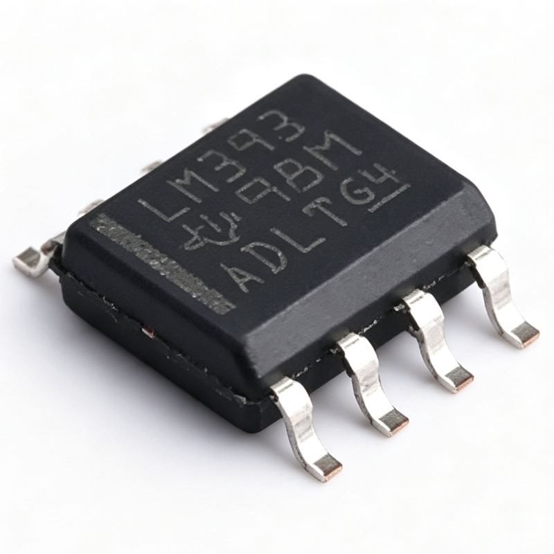
LM393DR - Dual Differential Comparator SOIC-8 | Texas Instruments
The Texas Instruments LM393DR is a dual differential comparator integrating two independent, high-gain precision comparators on a single monolithic chip in an 8-pin SOIC surface-mount package. It operates from a single supply of 2V to 36V or dual supplies of ±1V to ±18V, with an open-collector output stage that supports rail-to-rail output flexibility. A comparator is an analog component that compares two input voltages and drives its output to indicate which is higher. Within the component hierarchy, the LM393 belongs to the general-purpose comparator family (a cousin of the operational amplifier optimized for fast saturated switching), sitting alongside the LM339 quad and LM2903 automotive variants in the power-management and signal-conditioning landscape. Key features include very low supply current of approximately 0.4 mA per comparator, which does not increase with supply voltage, low input offset voltage (typically 1 mV), and a wide common-mode input range that extends down to ground (V-), enabling ground-sensing applications. The open-collector outputs allow wired-OR configurations and direct interface to logic families via a pull-up resistor to any voltage up to 36V, independent of the comparator supply. The LM393 architecture uses a PNP differential input stage on a proven junction-isolated bipolar process that has made it an industry standard for decades. Multiple manufacturers (TI, ROHM Semiconductor, and others) second-source the identical LM393DR ordering code, offering strong supply-chain resilience and true drop-in interchangeability. The improved LM393B version is a drop-in replacement offering lower offset (0.37 mV), lower bias current, and faster 1 us response time. Typical applications include voltage-level detection, zero-crossing detection, oscillator and square-wave generation, window comparators, battery undervoltage/overvoltage monitors, and limit comparators in industrial and consumer systems. It is a staple in power-supply supervisory circuits and sensor threshold detection, often paired with NE555 timer-based designs. Design consideration: always use a pull-up resistor (typically 1 kOhm to 100 kOhm) on each open-collector output, and add hysteresis (a few mV via positive feedback) to prevent output oscillation from slow-moving input signals near the threshold.

LSF0102-Q1 - 2-Ch Auto Bidirectional Level Translator | TI
The Texas Instruments LSF0102-Q1 is an automotive-qualified, 2-channel auto bidirectional multi-voltage level translator for open-drain and push-pull applications, packaged in an 8-pin VSSOP (DCU). It operates from 0.95 V to 5.5 V on Vref_A and 1.8 V to 5.5 V on Vref_B, enabling bidirectional translation between 0.95 V and 5.5 V without a direction pin. Data inputs are 5-V tolerant. A voltage level translator is a logic IC that converts signal voltage levels between circuits operating at different supply rails, sitting within the broader hierarchy of voltage translators -> logic ICs -> interface semiconductors. The LSF family uses a pass-gate (transmission-gate) architecture with reference rails, distinguishing it from powered translator families such as TXS/TXB that use MOSFET output stages. Key features include up to 100 MHz up translation and greater than 100 MHz down translation with capacitive loads of 30 pF or less; at a 50 pF load the device supports up to 40 MHz in both directions. This bandwidth covers standard automotive interfaces such as I2C, SPI, GPIO, SDIO, UART, and MDIO. AEC-Q100 qualification makes it suitable for automotive environments. The auto-direction architecture requires no direction-control pin, reducing MCU GPIO overhead and eliminating direction-timing errors. Because the LSF core is a passive pass-gate structure, external pull-up resistors set logic levels on open-drain buses; for push-pull signals, the reference rails Vref_A and Vref_B define the translated levels directly. Typical applications include automotive infotainment I2C buses between 1.8 V SoCs and 3.3 V peripherals, SPI connections between low-voltage MCUs and 5 V sensors, and SDIO/GPIO interfaces in body electronics and cluster modules. Design consideration: because the LSF topology needs external pull-up resistors on open-drain nets, size them against total bus capacitance and target rise time; keep capacitive loading at or below 30 pF to exploit the full 100 MHz translation rate.

LSF0102DDFR - 2-Ch 100Mbps Level Translator | TI
The Texas Instruments LSF0102DDFR is a dual-channel auto-bidirectional multi-voltage level translator supporting both open-drain and push-pull applications. Housed in an 8-pin TSOT-23-8 (DDF) package, it translates signals between voltage domains from 0.95V up to 5.5V at data rates up to 100 Mbps without requiring a direction control pin. A level translator, or voltage level shifter, is a logic IC that enables digital signals to safely cross between circuits operating at different supply voltages, such as 1.8V, 3.3V, and 5V domains. Within the hierarchy of logic ICs, translators sit alongside buffers and bus switches in the signal-interface layer of a system, ensuring reliable communication in mixed-voltage designs. Key features include fully automatic bidirectional translation with no direction pin, support for open-drain buses (I2C, SMBus) and push-pull interfaces (SPI, UART), a wide 0.95V to 5V translation range, and ultra-low quiescent current of 6 uA typical. The fast propagation delay preserves signal timing in high-speed links up to 100 Mbps. Technically, the LSF0102 uses a pass-gate (transmission-gate) architecture. The reference pins VREF_A and VREF_B set the logic levels on each side, and external pull-up resistors define the high levels of each domain. The device senses data direction automatically, making it transparent to the host system and reducing pin count and firmware complexity compared to directional translators. Typical applications include I2C and SMBus level shifting between 1.8V, 3.3V, and 5V domains, SPI and UART interfaces in mixed-voltage embedded systems, general-purpose GPIO translation, and battery-powered portable devices where the 6 uA quiescent current minimizes standby drain. Design consideration: pull-up resistor values directly trade off maximum data rate against power consumption; use lower resistance (1-2 kilohm) for high-speed push-pull operation and higher resistance (4.7-10 kilohm) for low-power open-drain buses.
MPC506 - 16-Ch ±15V CMOS Analog Multiplexer | Texas Instruments
The Texas Instruments MPC506 is a 16-channel single-ended CMOS analog multiplexer designed for precision analog signal routing in data acquisition and test systems. It operates with analog signal ranges up to ±15V and features internal overvoltage protection up to 70Vpp, ensuring robust performance in industrial environments. The device is available in a 28-pin SOIC package (MPC506AU) and is pin-compatible with the MPC507A differential 8-channel variant. An analog multiplexer is a semiconductor device that selects one of several analog input signals and routes it to a single output, controlled by digital address lines. It is a fundamental building block in data acquisition systems, enabling multiple sensors or signal sources to share a single ADC or amplifier. Multiplexers belong to the broader category of analog switches and are essential where signal routing, channel expansion, or test automation is required. Key features include break-before-make switching to prevent channel interaction, low standby power of 7.5mW typical, and a 1.5kOhm on-resistance. The device supports a ±15V analog signal range and provides overvoltage protection without channel interaction, making it suitable for harsh industrial environments. CMOS fabrication ensures low power consumption and high input impedance. Fabricated in CMOS technology, the MPC506 provides low leakage currents and high input impedance, preserving signal integrity. The internal 1kOhm series resistance protects the device from overvoltage conditions up to 70Vpp, eliminating external protection components in many applications. Break-before-make switching ensures the output is never momentarily connected to two inputs simultaneously, preventing signal corruption. Typical applications include data acquisition systems, test and measurement equipment, industrial process control, and medical instrumentation. The MPC506 is ideal for routing multiple analog signals to a single ADC, expanding channel count in a measurement system, or implementing programmable gain amplifier configurations. When designing with the MPC506, ensure analog input signals remain within the specified ±15V range to avoid damage. Drive the digital address lines with proper logic levels, and buffer the output if driving a capacitive load to maintain stability.
SN54HC157-SP - QML-V Quad 2:1 Multiplexer | Texas Instruments
The Texas Instruments SN54HC157-SP is a radiation-tolerant, QML-V qualified quadruple 2-line to 1-line data selector/multiplexer designed for space and high-reliability applications. It selects one of two 4-bit data sources via a common select input (A/B) and routes the chosen word to four outputs, with an active-low strobe input (G) that forces all outputs low for bus isolation. A data selector/multiplexer is a combinational logic circuit that forwards one of several input signals to a common output. Multiplexers are fundamental building blocks of digital data-path design, used for bus arbitration, register file selection, and redundant path switching. The SN54HC157-SP implements the 2-to-1 multiplexing function for four independent channels and belongs to the HC (high-speed CMOS) logic family, which combines CMOS low static power with TTL-compatible drive capability. Key features include a wide operating supply range of 2 V to 6 V, low power consumption with a maximum ICC of 80 uA, and outputs that can drive up to 15 LSTTL loads. Typical propagation delay is 11 ns, with balanced +/-6-mA output drive at 5 V operation. The device is qualified to QML-V (MIL-PRF-38535 Appendix V) standards for radiation tolerance, making it appropriate for satellite and deep-space missions. Technically, the device uses a CMOS process providing high noise immunity and low static dissipation. Internal inverters and drivers supply full data selection to the four output gates. When the strobe (G) is high, all outputs are forced low, simplifying bus isolation. Inputs accept standard CMOS levels and are TTL compatible at 5 V operation. Typical applications include data routing in spacecraft telemetry systems, selection between primary and backup data paths in redundant architectures, and switching between instrument outputs in satellite payloads to conserve downlink bandwidth. The -55C to +125C operating range and hermetic ceramic DIP (CDIP-16) packaging support these extreme environments. When designing with this device, decouple VCC close to the pins, drive the strobe input to a known state during power-up, and verify select and data inputs meet setup and hold requirements relative to the system clock, considering the 11 ns typical propagation delay.
SN54LS05 - Military 6-ch Open-Collector Inverter | TI
The SN54LS05 is a military-grade, 6-channel bipolar inverter with open-collector outputs, operating from a 4.5-V to 5.5-V supply. Manufactured by Texas Instruments, this device is designed for high-voltage, high-current interfacing and wired-OR logic applications. It comes in a 14-pin CDIP package, suitable for through-hole mounting in harsh environments. An inverter is a logic gate that outputs the logical complement of its input. The SN54LS05 specifically features open-collector outputs, meaning the output transistor's collector is left unconnected internally, requiring an external pull-up resistor to define the high-level output voltage. This allows the device to interface with different voltage domains and to implement wired-OR logic by connecting multiple outputs together. Open-collector outputs also enable driving loads such as relays, LEDs, and lamps directly, with appropriate current limiting. Key features include six independent inverters, a wide operating temperature range of -55°C to 125°C, and compatibility with TTL logic levels. The open-collector outputs can sink up to 8 mA, and the device supports a supply voltage range of 4.5 V to 5.5 V. The military-grade qualification ensures reliability in defense and aerospace applications. Technically, the SN54LS05 uses bipolar junction transistor (BJT) technology, providing fast switching speeds and robust output drive. The open-collector design allows for level shifting and bus communication, making it versatile for various logic interfacing tasks. The device is available in a 14-pin CDIP package, which offers excellent thermal and mechanical stability. Typical applications include military electronics, industrial control systems, and any design requiring high-voltage or high-current logic interfacing. The SN54LS05 is often used to drive relays, lamps, and other loads, as well as to implement wired-OR logic in bus systems. When designing with this device, ensure that pull-up resistors are properly sized to limit output current and to achieve the desired switching speed. The open-collector outputs require external pull-ups to VCC or another voltage rail, and the resistor value should be chosen based on the load capacitance and required rise time.
SN74ABT162841 - 20-Bit Bus-Interface D-Type Latch | TI
The SN74ABT162841 is a 20-bit bus-interface D-type transparent latch with 3-state outputs, designed by Texas Instruments as part of the Widebus family. It features noninverting outputs and is optimized for driving highly capacitive or relatively low-impedance loads. The device operates from a 4.5V to 5.5V supply, with a typical propagation delay of 4.6 ns and output ground bounce below 0.8V at VCC = 5V and TA = 25°C. It is available in a 56-pin SSOP package (DL suffix) and a 56-pin TSSOP package (DLR suffix). A bus-interface D-type latch is a digital logic component that captures data on its D inputs when the latch enable (LE) signal is asserted, holding the data on its Q outputs until the next enable pulse. It is a fundamental building block in digital systems for temporary data storage, bus isolation, and signal synchronization. In the hierarchy of digital logic, it belongs to the category of latches, which are level-sensitive storage elements, as opposed to edge-triggered flip-flops. Latches are essential in microprocessor systems, memory interfaces, and data acquisition circuits where multiple data lines must be captured simultaneously. Key features of the SN74ABT162841 include 3-state outputs that allow connection to a shared bus without contention, a flow-through architecture that simplifies PCB layout, and distributed VCC and GND pins that minimize high-speed switching noise. The device also supports hot insertion with Ioff and power-up 3-state, and its latch-up performance exceeds 500 mA per JEDEC standards. The EPIC-B BiCMOS design significantly reduces power dissipation compared to bipolar logic, making it suitable for high-density systems. Technically, the SN74ABT162841 uses a BiCMOS process that combines the speed of bipolar transistors with the low power of CMOS. The outputs have equivalent 25-ohm series resistors, eliminating the need for external resistors in many applications. The device is characterized for operation from -40°C to 85°C, and it is RoHS compliant. The 3-state outputs are controlled by an output enable (OE) input, which places the outputs in a high-impedance state when asserted high, allowing multiple devices to share a bus. Typical applications include memory address latching, data bus buffering in microprocessor systems, and interface circuits for industrial control and telecommunications equipment. The wide operating voltage range and high drive capability make it ideal for 5V systems that require robust signal integrity. The flow-through pinout aligns inputs and outputs on opposite sides, simplifying board routing and reducing crosstalk. When designing with this device, ensure that the OE and LE inputs are properly driven to avoid bus contention. The 3-state outputs allow multiple latches to share a bus, but only one should be enabled at a time. Consider the propagation delay and setup/hold times when designing timing margins for high-speed applications.
SN74ACT373-EP - Octal D-Type Transparent Latch | Texas Instruments
The SN74ACT373-EP is an Enhanced Product octal D-type transparent latch with 3-state outputs from Texas Instruments, designed for driving highly capacitive or relatively low-impedance loads. This 8-bit latch operates over a wide VCC range of 4.5V to 5.5V, with inputs that accept voltages up to 5.5V and are TTL-voltage compatible. The device features a buffered output-enable (OE) input that places the eight outputs in either a normal logic state or a high-impedance state, enabling bus-organized systems without the need for interface or pullup components. An octal D-type transparent latch is a digital logic component that captures the state of eight data inputs (1D-8D) when the latch-enable (LE) input is high, and holds that state when LE is low. The 3-state outputs allow multiple devices to share a common bus, as each output can be disabled (high-impedance) to avoid contention. This device is part of the ACT family, which combines advanced CMOS technology with TTL-compatible inputs, offering high speed and low power consumption. Key features include a maximum propagation delay (tpd) of 5V, 3-state outputs for bus driving, and compatibility with TTL voltage levels. The Enhanced Product designation indicates extended temperature range and reliability for demanding applications. The device is available in multiple package options, including SOIC, SSOP, TSSOP, and PDIP, providing design flexibility. Technically, the SN74ACT373-EP uses a CMOS process that provides balanced propagation delays and high noise immunity. The 3-state outputs are controlled by the OE input, which when low, enables the outputs; when high, places them in high-impedance state. This allows the latch to drive bus lines directly, reducing the need for external buffers. The device also features a latch-enable (LE) input that is level-sensitive, making it transparent when high and latched when low. Typical applications include address latching in microprocessor systems, data buffering in memory interfaces, and general-purpose I/O expansion. The high drive capability and 3-state outputs make it ideal for bus-oriented designs where multiple peripherals share a common data bus. The wide operating temperature range of -40°C to 125°C (Enhanced Product) ensures reliable operation in industrial and automotive environments. When designing with this device, ensure that the OE and LE inputs are properly driven to avoid bus contention. The high-impedance state should be used to prevent multiple outputs from driving the same bus simultaneously. Additionally, consider the propagation delay and setup/hold times to meet system timing requirements.
SN74AHC1G00DBVR - 2-5.5V Single 2-Input NAND Gate | Texas Instruments
The SN74AHC1G00DBVR is a single 2-input positive-NAND gate from Texas Instruments, designed for 2-V to 5.5-V operation. It performs the Boolean function Y = A NAND B in positive logic and is housed in a 5-pin SOT-23 (DBV) surface-mount package, making it ideal for space-constrained designs requiring low power and high noise immunity. A NAND gate is a fundamental digital logic gate that outputs LOW only when all inputs are HIGH. It is a universal gate, meaning any other logic function (AND, OR, NOT, XOR) can be built from NAND gates alone. The SN74AHC1G00 belongs to the AHC (Advanced High-Speed CMOS) logic family, which balances speed and power for battery-powered and portable systems within the broader CMOS logic IC hierarchy. Key features include a wide 2-V to 5.5-V operating range, a maximum propagation delay of 6.5 ns at 5 V, and maximum quiescent supply current of only 10 uA. Schmitt-trigger action on all inputs provides hysteresis-based noise immunity, allowing slow input edges without false triggering and eliminating external conditioning components. The device delivers ±8 mA output drive at 5 V, compatible with standard CMOS and TTL logic levels. Fabricated in advanced CMOS technology, the SN74AHC1G00 combines high-speed switching with low static and dynamic power dissipation. Robustness features include latch-up performance exceeding 250 mA per JESD 17 and ESD protection exceeding 2000-V HBM, 200-V MM, and 1000-V CDM ratings per the TI datasheet. Typical applications include signal gating, logic inversion, clock gating, and interface buffering in consumer electronics, industrial control, and automotive subsystems. The small SOT-23-5 footprint suits wearables, IoT modules, and dense PCBs where board area is at a premium. Design tip: do not let input voltages exceed VCC, and decouple the VCC pin with a 0.1-uF ceramic capacitor for best noise performance. Pricing shown reflects distributor data as of 2026-08-29.