Logic ICs
Products (88)
SN74HC4060 - 14-Stage Binary Counter & Oscillator | TI
The SN74HC4060 is a 14-stage asynchronous binary counter with an integrated oscillator section, manufactured by Texas Instruments. It operates over a wide voltage range of 2V to 6V, features a typical propagation delay of 14 ns, and can drive up to 10 LSTTL loads. The device is available in multiple package options including 16-SOIC (D), 16-PDIP (N), and 16-TSSOP (PW), making it suitable for a variety of PCB layouts. A binary counter is a digital circuit that counts in binary sequence, incrementing on each clock pulse. The SN74HC4060 specifically is an asynchronous (ripple) counter, meaning each stage's output triggers the next, resulting in a simple but effective frequency division. It belongs to the 74HC family of high-speed CMOS logic, which combines the low power consumption of CMOS with the speed of TTL. The oscillator section allows the device to generate its own clock signal using either an RC network or a crystal, eliminating the need for an external clock source. Key features include a 14-stage ripple-carry binary counter, an integrated oscillator supporting RC or crystal configurations, a master reset (CLR) input that disables the oscillator and clears the counter, and a clock input (CLKI) that increments the counter on high-to-low transitions. The device also offers a low input current of 1 µA max and a low power consumption of 80 µA max ICC, making it ideal for battery-powered applications. Technically, the SN74HC4060 uses high-speed CMOS technology, providing a balanced combination of speed and power efficiency. The oscillator section can be configured with external components to generate frequencies from sub-Hz to several MHz, depending on the RC or crystal values. The counter stages divide the oscillator frequency by powers of two, allowing precise frequency division for timing applications. The clear function ensures the counter can be reset to zero at any time, which is essential for synchronized operations. Typical applications include frequency dividers, timers, and oscillator circuits in consumer electronics, industrial control systems, and communication devices. For example, it can be used to generate precise time delays in microcontroller systems or to divide a crystal oscillator frequency down to a usable clock for peripherals. Its wide operating voltage range and robust output drive make it compatible with both 3.3V and 5V logic systems. When designing with the SN74HC4060, ensure that the oscillator components are placed close to the IC to minimize parasitic capacitance and noise. For crystal oscillators, use the recommended load capacitors as specified in the datasheet. Also, consider the counter's asynchronous nature, which may introduce glitches on outputs; adding output flip-flops can synchronize the count if needed.
SN74HCS126QPWRQ1 - Automotive Quad 3-State Buffer | TI
The Texas Instruments SN74HCS126QPWRQ1 is an AEC-Q100 qualified automotive quadruple bus buffer with 3-state outputs and Schmitt-trigger inputs, housed in a 14-pin TSSOP (PW) package rated from -40C to +125C. The device operates from a 2.0 V to 6.0 V supply and buffers four non-inverting 1-bit channels with active-high output-enable pins. A CMOS logic buffer is a digital building block that reproduces (non-inverting) a digital signal while providing isolation between a weak or noisy source and a heavier load. In the logic hierarchy, the SN74HCS126-Q1 belongs to the buffer / line driver family of the HC/HCS CMOS logic category, and bus buffers with 3-state outputs further add the ability to disconnect the output from the bus, enabling shared, multidrop data lines in microprocessor and automotive in-vehicle networking systems. Key differentiating features include Schmitt-trigger inputs with hysteresis that convert slow or noisy input transitions into clean, fast edges - essential in automotive environments with ground bounce and EMI; 3-state outputs that implement high-impedance bus sharing; low input hysteresis threshold spread across the 2.0 V to 6.0 V operating range; and a typical CMOS microamp-level quiescent current that minimizes system standby power. The device is qualified per AEC-Q100 Grade 1 for harsh automotive ambient temperatures. Technically, the HCS family combines high-voltage CMOS fabrication with input hysteresis, providing robust switching thresholds (VT+ / VT- spread) across supply voltage, temperature, and process corners. Output drive is balanced across the supply range, and outputs are disabled to high impedance whenever the OE pin is low, allowing multiple drivers on one bus with tri-state control. Power-up and power-down protection prevents bus contention during supply sequencing. Typical applications include automotive body electronics, CAN/LIN transceiver front-end buffering, level-shifted control signals in 12 V-derived rails, industrial PLC I/O, and generic bus-buffering between microcontrollers and peripheral modules where slow edges must be squared up. Design tip: do not let the OE pin float - tie unused enables to ground and unused inputs to VCC or GND; ensure each enabled output sources/sinks within the drive limits at the given VCC to keep VOL/VOH within datasheet margins. This page adds value beyond the manufacturer datasheet by synthesizing distributor pricing, drop-in same-footprint alternatives (HC126 variants, HCS125 siblings), and practical design notes in one place.

SN74HCS541PWR - Octal Buffer Schmitt 3-State TSSOP-20 | TI
The Texas Instruments SN74HCS541PWR is an octal buffer and line driver with Schmitt-trigger inputs, 3-state outputs, and a flow-through pinout, supplied in a 20-pin TSSOP (PW) package. It operates over a wide 2 V to 6 V supply range and is fully specified from -40C to +125C. What is an octal buffer/line driver? It is a digital logic IC providing eight independent buffer channels capable of driving bus lines or long PCB traces. The 3-state outputs allow each device to release the bus into a high-impedance state, enabling multi-device bus sharing, while Schmitt-trigger inputs add hysteresis that converts slow or noisy input edges into clean logic transitions. The SN74HCS541 belongs to the HCS (High-speed CMOS with Schmitt-trigger) logic family, combining CMOS low power with TTL-compatible drive. Key features include the 2 V to 6 V operating range for 3.3 V and 5 V mixed-voltage systems, typical 0.4 V input hysteresis at 4.5 V for superior noise immunity, dual active-low output enables (OE1 and OE2, both must be low to activate outputs), and only 20 uA typical quiescent current at 6 V. Outputs sink or source up to 6 mA at 4.5 V, suitable for driving LEDs, relays, or additional logic inputs. Fabricated in silicon-gate CMOS, the device balances switching speed with low power dissipation. The flow-through pinout places inputs on one side and outputs on the opposite side, simplifying PCB routing and reducing crosstalk in bus-oriented layouts. Typical applications include microcontroller bus buffering, memory address/data line driving, sensor signal conditioning, and interfacing 3.3 V logic to 5 V domains in industrial automation and automotive-adjacent systems. Design tip: control the OE pins carefully to avoid bus contention, place 0.1 uF decoupling capacitors close to VCC/GND, and keep input rise times below 500 ns at 2 V and 200 ns at 6 V for best performance.

SN74HCS541QPWRQ1 - AEC-Q100 Octal Buffer 3-State | TI
The Texas Instruments SN74HCS541QPWRQ1 is an automotive-qualified (AEC-Q100) octal buffer and line driver featuring eight non-inverting channels with 3-state outputs, Schmitt-trigger inputs, and a flow-through pinout, supplied in a 20-pin TSSOP (PW) package rated from -40C to +125C. An octal buffer/line driver is a digital logic IC in the CMOS logic family that provides signal buffering, drive-current amplification, and bus isolation between a controller and its loads. Within the logic hierarchy, it belongs to the buffer and line-driver category of specialty logic, sitting between simple gates and full bus transceivers. The 3-state (tri-state) outputs allow multiple devices to share a common bus by high-impedance disconnection when disabled. Key features include Schmitt-trigger inputs with hysteresis that tolerate slow or noisy input edges typical of automotive harnesses, wide VCC operation of the HCS Schmitt-CMOS family, two independent active-low output-enable pins (OE1 and OE2) for flexible bus control, and a flow-through pinout that simplifies PCB routing by keeping inputs on one side and outputs on the other. The Q1 grade ensures AEC-Q100 qualification and PPAP support for automotive designs. The HCS (HC with Schmitt input) architecture combines high-speed CMOS output drive with hysteresis-enhanced input stages, improving noise margin on long or filtered signal lines. Outputs are non-inverting, so logic polarity is preserved, making the device suitable for address and control bus buffering in MCU-based systems. Typical applications include automotive body electronics and ADAS control modules, buffering GPIO or SPI/control lines from MCUs such as the TMS320F2800xx series, industrial PLC I/O isolation, and level-tolerant interfacing to switches and sensors with slow edge rates. Design tip: tie both OE pins low for always-enabled operation, and keep VCC decoupling (100 nF ceramic) close to the supply pins; the Schmitt inputs allow RC-filtered inputs but do not eliminate the need for controlled signal routing.
SN74HCS86PWR - Quad 2-Input XOR Schmitt-Trigger Gate | TI
The Texas Instruments SN74HCS86PWR is a quadruple 2-input XOR (exclusive OR) gate with Schmitt-trigger inputs, supplied in a 14-pin TSSOP (PW) surface-mount package. It operates from a 2V to 6V supply and is fully specified from -40C to +125C for industrial environments. A logic gate is the fundamental building block of digital electronics, performing Boolean operations on binary inputs. The XOR gate outputs a high level only when an odd number of its inputs is high, making it essential for adders, parity generators and checkers, comparators, and programmable inverters. The SN74HCS86 belongs to the TI HCS family, which pairs CMOS low static power with Schmitt-trigger inputs for superior noise immunity - a drop-in upgrade path for the classic 74HC86. Key features include the wide 2V to 6V operating range, Schmitt-trigger inputs with hysteresis (typically around 0.5V at a 5V supply), CMOS technology for near-zero quiescent current, and balanced output drive. Per the TI datasheet, the device can drive loads up to 50 pF while meeting all datasheet specifications; larger capacitive loads are not recommended. Technically, the CMOS architecture provides high noise margins and negligible static current, while the Schmitt inputs use internal positive feedback to create hysteresis. This makes the part tolerant of inputs from mechanical switches, quadrature encoders, RC oscillators, and long wires with slow rise times - conditions that would cause a standard HC86 input to oscillate or multi-trigger. Typical applications include signal conditioning of noisy sensor or switch inputs, parity generation in serial communication links, crystal and RC oscillator circuits, frequency doubling (XOR with a delayed copy of itself), and digital comparator functions in industrial control, instrumentation, and automotive modules. Design tip: tie all unused inputs to a defined logic level (GND or VCC) to prevent floating nodes, and keep total capacitive load per output at or below 50 pF; add a buffer such as SN74LVC244A if heavier loads are required. Pricing references below are as of 2026-08-30.
SN74HCS86QPWRQ1 - Quad 2-Input XOR Gate, AEC-Q100 | TI
The Texas Instruments SN74HCS86QPWRQ1 is an automotive-qualified quadruple 2-input XOR (exclusive OR) gate with Schmitt-trigger inputs, supplied in a 14-pin TSSOP (PW) package. It operates from a wide 2 V to 6 V supply range and across a -40C to +125C ambient temperature range, per AEC-Q100 temperature grade 1 qualification. An XOR gate is a fundamental digital logic primitive in the combinational logic family of gates and inverters: its output is HIGH only when an odd number of inputs is HIGH, making it essential for adders, parity generation and checking, pseudo-random sequence generation, and signal comparison. The SN74HCS86-Q1 belongs to the HCS (HC with Schmitt) CMOS logic family, a modern low-power derivative of the classic 74HC high-speed CMOS series. The key feature distinguishing this device is its Schmitt-trigger inputs, which tolerate slow or noisy input edges that would cause oscillation in standard CMOS gates. The wide 2 V to 6 V operating range supports legacy 5 V systems as well as 3.3 V and lower-voltage rails. The device offers very low static power consumption typical of CMOS logic, and automotive-grade robustness with HBM ESD Level 2 and CDM ESD classification Level C6 per the TI datasheet (Rev. C). Because all four XOR gates are independent in a single package, the device consolidates parity trees, phase comparators, and code-comparison functions efficiently on board. Balanced drive capability and standardized TTL/CMOS-compatible thresholds at 5 V ease interfacing with microcontrollers and FPGAs. Typical applications include automotive body and powertrain modules, gate drivers for isolated communication schemes, parity checkers in serial links, frequency doublers, and XOR-based CRC generation in industrial systems. Design tip: keep unused inputs tied to VCC or GND (unused XOR gates may have inputs grounded) to prevent floating-node oscillation and excess current draw, and provide local 100 nF decoupling per TI logic application guidance.
SN74HCT74 - Dual D-Type Flip-Flop with Clear/Preset | TI
The SN74HCT74 is a dual D-type positive-edge-triggered flip-flop from Texas Instruments, featuring clear and preset inputs. It operates over a supply voltage range of 4.5V to 5.5V, making it compatible with TTL logic levels. The device is available in multiple package options including 14-pin DIP (N), SOIC (D), and TSSOP (PW), with the SN74HCT74N being a common through-hole variant. A D-type flip-flop is a fundamental sequential logic element that stores one bit of data. On the rising edge of the clock signal, the output (Q) takes the value of the data input (D). The SN74HCT74 contains two independent flip-flops, each with preset (PRE) and clear (CLR) inputs that asynchronously set or reset the outputs regardless of clock state. This makes it essential for building registers, counters, and state machines in digital systems. Key features include a wide operating voltage range of 4.5V to 5.5V, low power consumption with a maximum ICC of 40 µA, and the ability to drive up to 10 LSTTL loads. The typical propagation delay (tpd) is 15 ns at 5V, and the output drive capability is ±4 mA. The device is fully specified for operation from -40°C to 85°C, making it suitable for industrial applications. The SN74HCT74 uses HCT (High-Speed CMOS with TTL-compatible inputs) technology, which combines the low power of CMOS with the input thresholds of TTL. This allows direct interfacing with TTL logic without additional level shifting. The positive-edge-triggered design ensures reliable data capture, and the asynchronous preset and clear inputs provide flexible control for initialization and reset operations. Typical applications include data storage registers, frequency dividers, and control logic in microcontrollers, industrial automation, and consumer electronics. The device is also used in debouncing circuits and as a building block for more complex sequential logic. Its TTL compatibility makes it ideal for mixed-voltage systems. When designing with the SN74HCT74, ensure that the setup and hold times are met relative to the clock edge. The preset and clear inputs are active-low and should be tied high when unused. Decouple the power supply with a 0.1 µF capacitor near the VCC pin to minimize noise.

SN74LS138 - 3-to-8 Decoder/Demultiplexer LS-TTL | TI
The SN74LS138 is a 3-line to 8-line decoder/demultiplexer from Texas Instruments, part of the 74LS family of Schottky-clamped TTL MSI circuits designed for high-performance memory decoding and data-routing applications requiring very short propagation delay times. It provides three binary select inputs (A, B, C), three enable inputs (G1, G2A, G2B), and eight active-low outputs (Y0-Y7), operating from a 5V supply over 0C to +70C. A decoder is a combinational logic circuit that converts binary information from n input lines to a maximum of 2^n unique output lines. The 3-to-8 decoder is a fundamental building block in digital systems, used to select one of eight devices based on a 3-bit address. As an MSI device, it sits between SSI gates and LSI circuits in the digital logic hierarchy, and decoders are essential in memory address decoding where they enable specific memory chips. Key features include a typical propagation delay of 20 ns, low LS-TTL power dissipation (about 32 mW typical), and active-low outputs that sink up to 8 mA. The three enable inputs allow cascading multiple decoders into larger arrays (e.g., 4-to-16) and gating the device with control signals. Schottky-clamped TTL technology delivers high speed with good noise immunity and full TTL compatibility with 74LS, 74ALS, and 74AS families. The device is offered in 16-pin PDIP (N), SOIC (D), and SOP (NS) packages; the SN74LS138N in 16-PDIP is popular for through-hole and breadboard prototyping. According to the TI datasheet, the SN74LS138 is characterized from 0C to 70C for commercial operation. Typical applications include memory chip-select decoding in microprocessor systems, peripheral address decoding, and demultiplexing a single data line to one of eight outputs. Design tip: enable the device by driving G1 high and G2A/G2B low; tie unused inputs to valid logic levels to avoid floating nodes, and exploit the active-low outputs to drive active-low chip-select pins directly.

SN74LS145 - BCD-to-Decimal Decoder/Driver | Texas Instruments
The SN74LS145 is a monolithic BCD-to-decimal decoder/driver with open-collector outputs, designed to accept BCD inputs and provide appropriate outputs to drive 10-digit incandescent displays. It consists of eight inverters and ten four-input NAND gates, with the inverters connected in pairs to make BCD input data available for decoding by the NAND gates. Full decoding of valid BCD input logic ensures that all outputs remain off for all invalid binary input conditions. The device is available in a 16-pin PDIP package with through-hole mounting, making it suitable for legacy and new designs requiring high-voltage, high-current sinking capability. A BCD-to-decimal decoder is a combinational logic circuit that converts a 4-bit binary-coded decimal (BCD) input into one of ten decimal outputs. The SN74LS145 is a specific implementation that includes open-collector output transistors capable of sinking up to 80 mA at 15 V, allowing direct drive of relays, incandescent lamps, and other high-current loads. This decoder/driver sits within the broader hierarchy of digital logic ICs, specifically within the 74LS family of low-power Schottky TTL devices, which are known for their speed and compatibility with TTL, DTL, and MOS logic levels. Key features of the SN74LS145 include high-breakdown output transistors rated at 15 V, each capable of sinking up to 80 mA of current. Each input is one Series 54/74 or Series 54LS/74LS standard load, ensuring easy interfacing with other TTL logic. The open-collector outputs allow wired-OR connections and level shifting, providing design flexibility. The device operates over a wide supply voltage range and is compatible with standard TTL power supplies (5 V). The SN74LS145 uses low-power Schottky (LS) technology, which reduces power dissipation compared to standard TTL while maintaining high speed. The open-collector outputs are implemented with high-voltage transistors, enabling the device to drive loads connected to higher voltage rails (up to 15 V) while the logic operates at 5 V. This architecture is particularly useful in industrial control and display applications where loads require higher voltages than the logic supply. Typical applications include driving incandescent displays, relay drivers, and other high-current loads in industrial control systems, test equipment, and consumer electronics. The device is also used in BCD-to-decimal decoding for seven-segment displays, though it requires external current-limiting resistors. Its ability to sink 80 mA per output makes it suitable for driving relays and lamps directly, reducing the need for additional driver transistors. When designing with the SN74LS145, ensure that the output load current does not exceed the 80 mA rating and that the output voltage does not exceed 15 V. Pull-up resistors may be required when driving logic inputs from the open-collector outputs. The device is not recommended for new designs due to its obsolescence, but it remains available for legacy system maintenance.
SN74LV240A - Octal Inverting Buffer/Driver 3-State | TI
The SN74LV240A is an octal inverting buffer/line driver with 3-state outputs from Texas Instruments, designed for 2-V to 5.5-V VCC operation. It provides 8 mA of drive current at 3.3 V, making it ideal for bus interface applications where data retention or latching is required. The device features inverted outputs and is optimized for 3-state memory address drivers, clock drivers, and bus-oriented receivers/transmitters. An octal buffer/driver is a digital integrated circuit that provides eight independent buffering channels, each capable of driving a bus line with high current and low output impedance. The 3-state outputs allow the device to be disconnected from the bus (high-impedance state) when not active, enabling multiple devices to share the same bus without contention. This category sits within the logic IC family, specifically under buffers/drivers, which are essential for signal conditioning and bus isolation in digital systems. Key features include a wide operating voltage range of 2 V to 5.5 V, low power consumption typical of LV CMOS technology, and high drive capability of 8 mA at 3.3 V. The device supports mixed-mode voltage operation on all ports, allowing interfacing between different voltage domains. It also features latch-up performance exceeding 250 mA per JESD 17 and robust ESD protection, ensuring reliability in harsh environments. The SN74LV240A is fabricated using low-voltage CMOS technology, which provides a balance between speed and power dissipation. The 3-state outputs are controlled by an output-enable (OE) input, allowing the outputs to be placed in a high-impedance state for bus sharing. The inverting outputs provide signal inversion, which can simplify logic design in certain applications. The device is available in multiple package options, including SOIC, SSOP, and TSSOP, offering flexibility for various PCB layouts. Typical applications include memory address drivers, clock drivers, bus-oriented receivers/transmitters, and general-purpose digital interfacing. The low drive current and low noise characteristics make it suitable for low-noise applications where signal integrity is critical. The wide voltage range allows operation in both 3.3-V and 5-V systems, making it a versatile choice for mixed-voltage designs. When designing with the SN74LV240A, ensure proper decoupling capacitors are placed near the VCC and GND pins to minimize power supply noise. The OE pin should be tied to a defined logic level to avoid floating outputs, which can cause excessive power consumption or bus contention. Consider the propagation delay and output transition times when interfacing with high-speed buses to avoid timing violations.

SN74LV3T99-Q1 - 3ch Configurable Gate, 1.8-5.5V | TI
The Texas Instruments SN74LV3T99-Q1 is an automotive-grade, ultra-configurable multiple-function gate containing three independent configurable logic gates with 3-state outputs. Each gate has four inputs and implements the Boolean function Y = (A • /C + B • C) ⊕ D, with all inputs including Schmitt-triggers to eliminate erroneous data outputs caused by slow-edged or noisy input signals. The device operates from 1.8V to 5.5V and is offered in a 20-pin TSSOP (PW) package, with a 20-pin VSSOP (DGS) variant available. The -Q1 suffix denotes AEC-Q100 qualification for automotive applications. Configurable logic gates are digital ICs that let designers implement multiple logic functions in a single device, selected by pin strapping. They belong to the broader standard logic IC family - fundamental building blocks providing glue logic, level shifting, and signal conditioning in digital systems. The SN74LV3T99-Q1 sits within the LV (Low-Voltage) CMOS family and additionally functions as a logic-level shifter between voltage domains. Key features include three independent four-input gates with 3-state outputs for bus-oriented applications, Schmitt-trigger inputs providing hysteresis for superior noise immunity, and a wide 1.8V to 5.5V supply range enabling translation between 1.8V, 2.5V, 3.3V, and 5V logic families. AEC-Q100 qualification guarantees operation from -40C to +125C per automotive reliability requirements. Technically, the device uses CMOS technology for low static power consumption and high noise immunity. The configurable architecture replaces multiple discrete gates with one device, reducing board space and BOM count. The Boolean function supports MUX, AND, OR, NAND, NOR, XOR, XNOR, inverter, and buffer configurations - 16 output patterns determined by the 4-bit input when OE is low - while the output-enable (OE) input permits multiple devices to share a common bus through a high-impedance state. Typical applications include automotive body control modules, infotainment systems, and industrial automation, where the device handles signal conditioning, level shifting, and custom logic. The Schmitt-trigger inputs reliably interface sensors, switches, and microcontrollers in noisy environments. Test and measurement equipment also uses configurable logic for signal routing and control. Design tip: place 0.1uF decoupling capacitors close to the power pins, and carefully control the 3-state output-enable signals to avoid bus contention.

SN74LVC1G07DBVR - Open-Drain Buffer 1.65-5.5V SOT-23-5 | TI
The Texas Instruments SN74LVC1G07DBVR is a single non-inverting buffer/driver with an open-drain output, operating from a 1.65 V to 5.5 V supply, sinking up to 32 mA at 3.3 V, and housed in a 5-pin SOT-23-5 (DBV) surface-mount package. An open-drain buffer is a logic element whose output transistor has no internal pull-up structure; the output can only actively pull LOW and relies on an external pull-up resistor to another voltage rail to go HIGH. In the voltage-regulation hierarchy of digital logic families, this places the SN74LVC1G07 among low-voltage CMOS (LVC) interface logic, one step above raw gates and one step below full bus transceivers. Open-drain outputs are the foundation of shared buses such as I2C, interrupt lines, and wired-OR / wired-AND logic networks. Key features include support for 5 V VCC operation with input and open-drain output tolerating up to 5.5 V, a maximum propagation delay of 3.3 ns at 3.3 V, ultra-low power consumption with 10 uA maximum ICC, and ±24 mA output drive capability at 3.3 V. The Ioff feature supports partial-power-down applications by preventing damaging backfeed currents when the device is unpowered. Architecturally, the device combines a single CMOS input stage with a discrete NMOS pull-down output stage. Because the output floats high only through the external pull-up, multiple SN74LVC1G07 outputs can be tied together to implement active-low wired-OR or active-high wired-AND functions without contention. The wide 1.65 V to 5.5 V operating range allows true level-shifting: a 1.8 V logic signal can control a 5 V rail through the open-drain output. Typical applications include I2C and SMBus bus buffering, open-drain interrupt or enable line fan-out, level shifting between mixed-voltage subsystems, LED and relay driver front-ends, and microcontroller GPIO expansion where multiple boards share a common pull-up rail. Design consideration: the external pull-up resistor value is a trade-off - lower values improve edge speed and noise immunity but increase sink current; verify the resistor keeps the sink current below the 32 mA maximum rating. This page synthesizes distributor pricing, drop-in cross-brand alternatives, and practical design notes not found in the manufacturer datasheet.
SN74LVC1G07DCKR - 1.65V-5.5V Open-Drain Buffer SC-70-5 | Texas Instruments
The Texas Instruments SN74LVC1G07DCKR is a single non-inverting buffer/driver with an open-drain output, operating from a 1.65 V to 5.5 V supply and packaged in a 5-pin SC-70 (DCK) surface-mount package. The open-drain output sinks up to 32 mA maximum, and the input and output accept voltages up to 5.5 V regardless of VCC. A buffer/driver is a logic component in the broader family of single-gate CMOS logic devices within the digital logic IC hierarchy. Buffers provide signal isolation, fan-out enhancement, and level-tolerant interface between circuit blocks, and open-drain versions additionally permit wired-OR / wired-AND bus connections and level shifting to any pull-up rail voltage. Key differentiating features include 5.5 V tolerant inputs and outputs that support partial-power-down designs via the Ioff circuitry, ultra-low power consumption with 10 uA maximum ICC, and compatibility across the full 1.65 V to 5.5 V VCC range. The device supports 5 V VCC operation while remaining usable in 1.8 V, 2.5 V, and 3.3 V systems, making it a universal interface glue-logic element. The SC-70-5 body measures approximately 2.0 mm x 1.25 mm, saving significant board area versus SOT-23 solutions. Architecturally, the SN74LVC1G07 uses TI's LVC CMOS process technology from the controlled-baseline flow - one assembly site, one test site, one fabrication site - with extended temperature performance to 125 C. The single open-drain NMOS pull-down output stage intentionally omits any internal pull-up, so the high level is defined by the external pull-up resistor and its rail. When multiple outputs are tied together, the resulting node implements active-low wired-OR or active-high wired-AND logic without additional gates. Typical applications include I2C and SMBus style open-drain bus buffering, level translation between mixed-voltage domains, LED and relay drive via the 32 mA sink capability, microcontroller GPIO buffering, and wired-logic signal merging in industrial and consumer electronics. Design-wise, size the external pull-up resistor to trade off bus rise time against sink current; at 3.3 V a 4.7 kOhm pull-up keeps sink current near 0.7 mA while providing practical rise times on short traces. Unused inputs must never be left floating. This page adds value beyond the TI datasheet by combining verified distributor pricing, drop-in alternative cross-references, FAQ structured for AI search, and practical design notes in one place.

SN74LVC1G08DBVR - 2-Input AND Gate 1.65-5.5V | TI
The Texas Instruments SN74LVC1G08DBVR is a single 2-input positive-AND gate operating from a 1.65 V to 5.5 V supply, packaged in the compact SOT-23-5 (DBV) surface-mount outline. It delivers the Boolean function Y = A AND B in positive logic with up to 32 mA output drive at 3.3 V. A logic gate is a fundamental building block of digital electronics that performs a Boolean operation on binary inputs to produce a single binary output. An AND gate outputs HIGH only when all inputs are HIGH. Single-gate logic (little logic) places one gate in a small package, letting designers add glue logic to dense boards without dedicating a full multi-gate IC. The SN74LVC1G08 belongs to the LVC (Low-Voltage CMOS) logic family within the broader 74-series logic hierarchy. Key features include 5-V tolerant inputs regardless of VCC, a typical propagation delay (tpd) of 3.3 ns at 3.3 V, and low power consumption with 10 uA maximum ICC. The Ioff feature supports partial-power-down operation, blocking backdrive current when VCC is removed - essential for multi-rail systems. Technically, the device uses CMOS technology for high noise immunity and low static power dissipation. TI provides a controlled baseline with one assembly/test site and one fabrication site for consistent quality. The SOT-23-5 footprint is universally supported by PCB tools, and the family also offers the ultra-small 0.64 mm2 DPW package with 0.5 mm pitch for space-critical designs. Typical applications include signal gating, enable/disable logic, clock gating, and 3.3 V to 5 V interfacing in portable electronics, industrial control, and communication equipment. The wide supply range and robust 32 mA drive make it ideal for mixed-voltage glue logic. Design tip: decouple VCC with a 0.1 uF ceramic capacitor close to the device and tie unused inputs to a defined logic level - floating CMOS inputs can oscillate and draw excess current. Pricing references are as of 2026-08-30.
SN74LVC1G125DBVR - 3-State Buffer 1.65-5.5V | TI | SOT-23-5
The Texas Instruments SN74LVC1G125DBVR is a single non-inverting bus buffer gate with 3-state output, operating from a 1.65-V to 5.5-V supply in a compact SOT-23-5 (DBV) package. It buffers one bit with an active-low output-enable (OE) pin that places the output in high impedance when high. A bus buffer gate is a digital logic component that isolates or buffers a signal line, providing a high-impedance output when disabled so multiple devices can share a common bus without contention. The SN74LVC1G125 belongs to the LVC (Low-Voltage CMOS) logic family, part of the broader CMOS logic IC category known for low power and high speed. Key features include 5-V VCC operation with inputs accepting voltages up to 5.5 V, maximum propagation delay (tpd) specified at 3.3 V, and plus/minus 24-mA output drive at 3.3 V. The Ioff feature supports partial-power-down mode operation, preventing back-feeding current when the device is unpowered. Maximum ICC is only 10 uA, suiting battery-powered designs. The CMOS architecture delivers low static power with fast switching, and the wide 1.65-V to 5.5-V range enables level buffering in mixed-voltage systems such as 1.8-V to 3.3-V or 3.3-V to 5-V interfaces. According to the TI datasheet, the device drives capacitive loads up to 50 pF while meeting all datasheet specifications; TI recommends adding a series resistor between the output and the load for larger capacitances to prevent excessive current. Typical applications include logic level shifting, bus isolation in multi-board systems, signal buffering for industrial control, consumer electronics, and communication interfaces such as I2C, SPI, and UART lines. When designing, ensure the OE pin is properly driven to avoid bus contention, and add a series resistor for capacitive loads above 50 pF per TI datasheet guidance. The device operates from -40C to +125C. Pricing starts at approximately $0.41 at single-unit quantities as of 2026-08-30.

SN74LVC1G125QDBVRQ1 - AEC-Q100 Buffer, 3-State, SOT-23-5 | TI
The Texas Instruments SN74LVC1G125QDBVRQ1 is an automotive-catalog (Q1) single non-inverting bus buffer gate with a 3-state output, operating from a 1.65V to 5.5V supply in a 5-pin SOT-23 (DBV) package. The output is disabled (high-impedance) when the active-low output-enable (OE) pin is driven HIGH. A single-bus buffer gate is a logic device in the voltage-level and drive-strength hierarchy of digital ICs: buffer gate -> line driver -> bus-interface logic. Its role is to restore signal edges, increase fan-out, and isolate bus segments without inverting logic polarity. Key features include 5.5V-tolerant inputs for mixed-voltage environments, high output drive from advanced CMOS technology, and robust ESD protection rated at 2000V HBM, 200V MM, and 1000V CDM per the datasheet. The Q1 suffix denotes AEC-Q100 qualification and customer-specific configuration control, making the device suitable for automotive body, cluster, and infotainment modules. Fabricated on TI's advanced CMOS LVC process, the buffer achieves high speed with low power consumption and balanced drive in both push-pull directions. The NanoStar/NanoFree small-footprint SOT-23-5 package supports dense PCB layouts while maintaining 5V VCC operation capability. Typical applications include automotive CAN/LIN module I/O buffering, level-compatible bus isolation at 3.3V and 5V, MCU GPIO line driving, and sensor signal gating in 12V automotive electronic control units. Design tip: tie the OE pin to GND for a permanently enabled buffer; never leave OE floating, as the active-low enable polarity differs from the SN74LVC1G126 variant.
SN74LVC1G14DBVR - Schmitt Inverter 1.65-5.5V SOT-23-5 | TI
The Texas Instruments SN74LVC1G14DBVR is a single Schmitt-trigger inverter operating from a 1.65 V to 5.5 V supply, performing the Boolean function Y = NOT A. Housed in a 5-pin SOT-23 (DBV) NanoStar package, it delivers clean output transitions even with slow or noisy input signals, with +/-32 mA output drive at 3.3 V. A Schmitt-trigger inverter is a logic gate that uses positive feedback to create hysteresis between the positive-going threshold (VT+) and the negative-going threshold (VT-). This hysteresis (delta VT) prevents output chatter when the input hovers near the switching point, making the device tolerant of slow edges and noisy signals. Within the digital logic hierarchy, it is a fundamental inverter/combinational-logic building block used for buffering, waveform shaping, and signal conditioning. Key features include a wide 1.65 V to 5.5 V supply range compatible with 1.8 V, 2.5 V, 3.3 V, and 5 V logic families, high output drive of +/-32 mA at 3.3 V, and low typical quiescent current of about 10 uA. Partial power-down (Ioff) protection keeps outputs high-impedance when VCC is off, enabling safe mixed-voltage and hot-insertion designs. ESD protection is rated 2 kV HBM per the TI datasheet. Fabricated in TI's LVC CMOS technology, the device achieves propagation delays as low as 3.7 ns at 3.3 V with fully specified Schmitt thresholds across the supply range. It operates from -40 C to +125 C, suiting industrial and harsh-environment systems. NanoStar packaging keeps the footprint minimal for high-density boards. Typical applications include debouncing mechanical switches, conditioning slow or noisy sensor signals, building relaxation oscillators, and level-tolerant glue logic between voltage domains. The wide supply range and strong drive make it a versatile single-gate choice. Design tip: decouple VCC with a 0.1 uF ceramic capacitor placed close to the pin, and keep input traces short in high-speed sections to limit parasitic pickup. Prices as of 2026-08-30.
SN74LVC1G17DBVR - Schmitt-Trigger Buffer 5.5V | TI
The Texas Instruments SN74LVC1G17DBVR is a single Schmitt-trigger buffer operating from 1.65 V to 5.5 V, providing one non-inverting buffer (Boolean function Y = A) with push-pull output in a 5-pin SOT-23-5 (DBV) surface-mount package. A Schmitt-trigger buffer is a logic device that uses positive feedback to create hysteresis, giving it two distinct switching thresholds for rising and falling edges. Within the logic IC hierarchy, it belongs to the buffer/line-driver family of standard logic, used to isolate, drive, and condition digital signals. Hysteresis makes it ideal for cleaning up noisy signals, squaring off slow edges, and converting slowly changing analog inputs into crisp digital logic levels. Key features include the wide 1.65 V to 5.5 V supply range for compatibility with 3.3 V and 5 V systems, high CMOS output drive of up to 32 mA at 3.3 V, and low static power dissipation. The device is fully specified for partial-power-down applications using Ioff, which prevents damaging backflow current when VCC is removed. Per TI datasheet, the same die is also available in the ultra-small 0.64 mm2 DPW package with 0.5 mm pitch and in SC70 options. The SN74LVC1G17 is fabricated in CMOS technology, combining high-speed operation with low power. Schmitt-trigger inputs provide typical hysteresis of approximately 0.4 V at 3.3 V, ensuring clean switching with slow or noisy inputs, while the push-pull output directly drives LEDs, relay drivers, or downstream logic inputs without external pull resistors. Typical applications include sensor signal conditioning, switch debouncing, level shifting between logic families, oscillator circuits, and clock buffering in industrial and consumer designs spanning both 3.3 V and 5 V rails. Design tip: keep input signals within the supply range to avoid latch-up, and place the device close to the signal source to minimize trace inductance in high-speed paths. Pricing and stock data are current as of 2026-08-30.
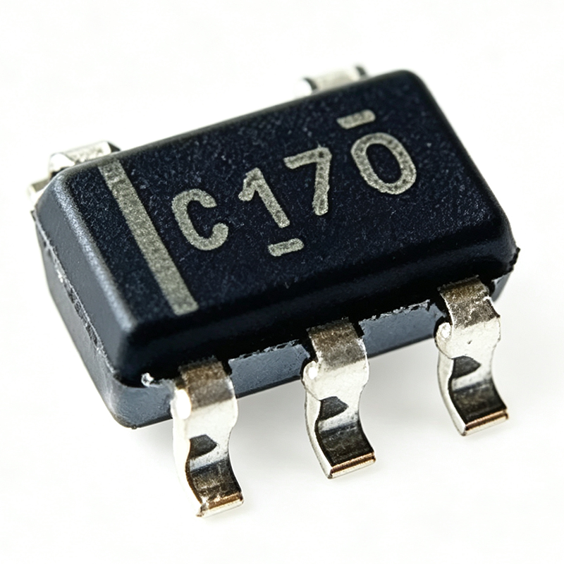
SN74LVC1G17QDBVRQ1 - Auto Schmitt Buffer SOT-23-5 | Texas Instruments
The Texas Instruments SN74LVC1G17QDBVRQ1 is an automotive-qualified (AEC-Q100) single Schmitt-trigger buffer designed for 1.65V to 5.5V VCC operation in a 5-pin SOT-23 (DBV) package. It performs the Boolean function Y = A and delivers high output drive while maintaining low static power dissipation across the full supply range. A Schmitt-trigger buffer is a logic device in the buffer/driver family of the standard CMOS logic IC hierarchy. Unlike a plain buffer, its input incorporates hysteresis, meaning the switching thresholds for rising and falling edges differ. This makes the device tolerant of slow or noisy input edges that would cause multiple transitions (oscillation) in conventional CMOS inputs, conditioning signals from RC timing circuits, sensor outputs, or long cables. Key features include the wide 1.65V to 5.5V operating supply range enabling use in mixed 1.8V/3.3V/5V systems, Schmitt-action inputs for noisy or slow-rising signals, push-pull output with high drive capability, and operation across the extended -40C to +125C automotive temperature range. The device belongs to TI's controlled-baseline LVC family with one assembly, one test site, and one fabrication site for consistent quality. The CMOS LVC architecture achieves low static power dissipation with fast propagation delay (typical values around a few nanoseconds depending on VCC; the digchip summary lists 10.7 ns at low supply). The DBV SOT-23-5 package is a compact surface-mount option for space-constrained designs. Typical applications include automotive ECU level translation and signal buffering, switch debouncing with hysteresis, RC oscillator waveform squaring, sensor signal conditioning, and general-purpose buffering in body electronics, infotainment, and industrial modules. Design tip: use the Schmitt hysteresis deliberately - pairing this buffer with a slow RC-filtered input (for example, from a comparator-less analog threshold) yields a clean digital edge; keep VCC decoupling (100 nF ceramic) close to the pin for signal integrity.
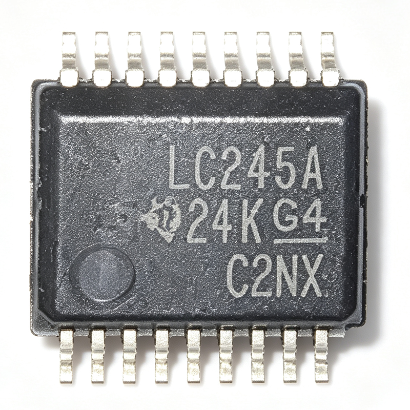
SN74LVC240A - Octal Inverting Buffer 3-State LVC | TI
The Texas Instruments SN74LVC240A is an octal inverting buffer/line driver with 3-state outputs, organized as two independently enabled 4-bit banks operating from a 1.65 V to 3.6 V supply. It is designed specifically to improve the performance and density of 3-state memory address drivers, clock drivers, and bus-oriented receivers and transmitters. An octal buffer/line driver is a digital logic IC in the 74xx logic family that provides signal buffering, inversion, and bus isolation. Within the logic-IC hierarchy, the SN74LVC240A belongs to the Low-Voltage CMOS (LVC) technology family, a subfamily of 74-series logic. Its 3-state outputs allow multiple devices to share a common bus without contention, a fundamental requirement in bus-oriented digital systems such as memory subsystems and backplanes. Key features include 5.5-V tolerant inputs enabling mixed-mode signal operation on all ports (5-V input/output voltage support), a typical propagation delay (tpd) of 3.3 ns at VCC = 3.3 V, and low typical VOLP (output ground bounce) and VOHV (output VOH undershoot) figures for superior signal integrity. According to the TI datasheet (SCAS293), the device can drive a load with total capacitance less than or equal to 50 pF while still meeting all datasheet specifications. The device is built on advanced CMOS technology, combining low static power consumption with high noise immunity and strong output drive. The dual-bank structure with separate active-low output-enable (OE) inputs supports half-duplex transceiver topologies and word-wide bus gating. When OE is low, data passes from the A inputs to the inverted Y outputs; when OE is high, outputs enter the high-impedance state. Typical applications include 3-state memory address and clock driving, 3.3-V to 5-V mixed-voltage bus interfacing, industrial control I/O buffering, and telecom line-card logic. Packages include SOIC-20 (DW), TSSOP-20 (PW), and SSOP-20 (DB). Design tip: keep total capacitive load at or below 50 pF for guaranteed timing, add 0.1 uF decoupling per supply pin, and tie unused inputs to VCC or GND to prevent floating-node oscillation.
SN74LVC244APWR - Octal Buffer 3-State 24mA | TI | Bus Driver
The Texas Instruments SN74LVC244APWR is an octal buffer/line driver with 3-state outputs, designed for 1.65-V to 3.6-V VCC operation in a 20-pin TSSOP (PW) package rated from -40C to +125C. Organized as two 4-bit non-inverting buffers with separate active-low output-enable (OE) inputs, it provides asynchronous communication between data buses. A buffer/line driver is a digital logic IC that provides signal amplification, isolation, and fan-out between system blocks. Within the logic IC hierarchy, it belongs to the standard logic family alongside transceivers, latches, and flip-flops. The 3-state output feature lets the device disconnect from a shared bus, enabling multiple drivers to share a common data line without bus contention. Key features include a wide 1.65-V to 3.6-V supply range covering both 1.8-V and 3.3-V logic domains, inputs that tolerate voltages up to 5.5 V for mixed-voltage systems, and +/-24 mA output drive at 3.3 V. The Ioff partial-power-down circuitry prevents damaging backflow current when VCC is removed, and latch-up performance exceeds 100 mA per JESD 78 Class II. ESD protection exceeds 2000-V HBM (JESD 22 A114-A) and 1000-V CDM. Fabricated in advanced CMOS, the SN74LVC244A achieves a typical propagation delay of 4.3 ns at 3.3 V while maintaining low static power consumption, balancing speed and efficiency for bus-interface timing budgets. Typical applications include memory address buffering, clock distribution, and general-purpose I/O expansion for microcontrollers, FPGAs, and DSPs, plus level shifting between 1.8-V and 3.3-V domains in industrial control and telecommunications equipment. Design tip: decouple VCC with a 0.1-uF ceramic capacitor placed close to the pin, tie unused OE pins to a defined logic level, and keep traces short for high-speed signals.
SN74LVC244QAPWRQ1 - Auto 8-Bit 3-State Buffer | TI
The Texas Instruments SN74LVC244QAPWRQ1 is an automotive-qualified (AEC-Q100) octal buffer/driver with 3-state outputs, organized as two independent 4-bit sections with separate output-enable (OE) inputs. It operates from a 1.65 V to 3.6 V supply in a 20-pin TSSOP (PW) surface-mount package with tape-and-reel packing. An octal buffer is a digital logic device that strengthens (buffers) eight signal lines at once, providing higher output drive and isolation between a controller and a load. Within the logic hierarchy, it belongs to the buffer/driver family of CMOS logic ICs, positioned above single-gate buffers and below bus transceivers, which add bidirectional capability. Key features include fully 3-state outputs for shared-bus connections, individual OE control for each 4-bit half, LVC-family CMOS technology supporting partial-power-down operation with Ioff protection, and an operating temperature range of -40C to +125C suitable for automotive and industrial environments. According to the TI SN74LVC244A-Q1 datasheet (Rev. D), the device performs the non-inverting buffer function Y = A for each channel. The LVC process provides low quiescent current, TTL-compatible input thresholds at 3.3 V operation, and balanced output drive for typical 24 mA-class loads at 3.3 V, making it suitable for address/data bus driving, clock distribution, and level-stable signal buffering between a microcontroller and peripherals. Typical applications include automotive body control modules, gateways and infotainment buses, industrial PLC I/O isolation, and memory or peripheral chip-select driving in embedded systems. Design tip: tie unused OE inputs to VCC through a pull-up resistor so outputs stay in the high-impedance state during power-up, and decouple the VCC pin with a 0.1 uF ceramic capacitor placed within 2 mm of the pin to suppress transient currents during simultaneous switching.

SN74LVC2G17 - Dual Schmitt-Trigger Buffer 5.5V | Texas Instruments
The Texas Instruments SN74LVC2G17 is a dual Schmitt-trigger buffer designed for 1.65-V to 5.5-V VCC operation, performing the Boolean function Y = A on two independent channels. Packaged in the popular SOT-23-6 (DBV), SON-6 (DRY), and NanoStar (YEP) options, it suits space-constrained designs requiring noise-tolerant signal buffering. A Schmitt-trigger buffer is a digital logic gate that uses positive feedback to create different input thresholds for rising (VT+) and falling (VT-) signals. This hysteresis eliminates false triggering from noise or slow input edges, making Schmitt buffers essential for conditioning noisy signals, debouncing mechanical switches, and squaring up slow-rise-time waveforms. The SN74LVC2G17 belongs to the LVC logic family, part of the broader low-voltage CMOS buffer and line-driver category in the logic IC hierarchy. Key features include a wide supply range of 1.65 V to 5.5 V, 5.5-V input tolerance for mixed-voltage interfacing, and a maximum propagation delay (tpd) of 3.3 ns at 3.3 V. Output drive is ±24 mA at 3.3 V with a push-pull stage providing rail-to-rail output swing. Maximum ICC is 10 uA, enabling low-power designs, and the Ioff feature fully supports partial-power-down operation by preventing damaging backflow current when VCC is removed. Architecturally, the device uses a CMOS process with comparator-based Schmitt input circuits that guarantee stable switching even with very slow input transitions. Typical VOLP (output ground bounce) and VOHV (output VOH undershoot) are specified at 25C to characterize system-level signal integrity. Both an automotive SN74LVC2G17-Q1 (AEC-Q100 qualified) variant and the enhanced SN74LVC2G17-EP for demanding applications are available. Typical applications include switch debouncing, sensor signal conditioning, level shifting between 3.3-V and 5-V logic domains, and buffering of slow or noisy signals in industrial, consumer, and automotive electronics. Design tip: leverage the hysteresis characteristics for your noise environment and observe proper power sequencing - Ioff supports partial power-down, but unintended current paths should still be avoided.
SN74LVC2G34DCKR - Dual Buffer 1.65-5.5V SC-70-6 | Texas Instruments
The Texas Instruments SN74LVC2G34DCKR is a dual non-inverting buffer gate designed for 1.65-V to 5.5-V VCC operation, performing the Boolean function Y = A in positive logic. It comes in a compact 6-pin SC-70 (DCK) surface-mount package measuring 2.0 mm x 1.25 mm with a 0.65-mm pin pitch. A buffer gate is a digital logic circuit that amplifies or isolates a signal without changing its logic level. In the logic IC hierarchy, it falls under gates within the 74LVC CMOS logic family, ultimately classified as a standard logic integrated circuit. Buffers increase fan-out, drive longer PCB traces, and provide impedance isolation between a signal source and its load. Key features include support for 5-V VCC operation, inputs tolerant up to 5.5 V regardless of supply, and a typical propagation delay (tpd) of 3.3 ns at VCC = 3.3 V. Output drive is +/-24 mA at 3.3 V, ensuring solid signal integrity. Maximum ICC is only 10 uA, making the part ideal for battery-powered designs. The device is fully specified for partial-power-down applications using Ioff circuitry, which disables outputs to prevent damaging backflow current when VCC is removed. The SN74LVC2G34 uses a CMOS process delivering high noise immunity and low static power dissipation. Typical VOLP (output ground bounce) and VOHV (undershoot) performance keeps switching noise minimal in mixed-signal boards. NanoStar and NanoFree package technologies are available in the family for ultra-miniature footprints. Typical applications include MCU GPIO buffering, clock distribution, level-compatible interfacing between 3.3-V and 5-V domains, and general logic isolation in consumer, industrial, and communication equipment. Pair it with TI translation parts such as TXS0102-Q1 or SN74LVC1T45 for full level shifting. Design tip: decouple VCC with a 0.1-uF ceramic capacitor close to the pin, and keep buffered traces short and impedance-controlled to preserve the 3.3-ns speed advantage.