Power MOSFET Drivers
Products (426)

TPS22997RYZR - 5.5V 10A 4mOhm Load Switch | Texas Instruments
The Texas Instruments TPS22997RYZR is a single-channel load switch with an integrated N-channel MOSFET, operating over an input voltage range of 0.1 V to 5.5 V and supporting a maximum continuous current of 10 A, with a typical on-resistance of 4 mOhm. It is housed in a compact 10-WQFN-HR (1.5x2 mm) package designed for space-constrained, high-current power distribution. A load switch is a semiconductor device that connects or disconnects a power supply rail from a load, functioning as an electronic switch. It typically integrates a pass MOSFET, gate-drive control logic, and protection features such as thermal shutdown and inrush management. Load switches sit within the power management IC hierarchy alongside hot-swap controllers and eFuses, and are essential for power gating, rail sequencing, and protection in systems from smartphones to industrial equipment. Key features include adjustable slew rate control to minimize inrush current during turn-on, adjustable quick output discharge (QOD) for rapid discharge of output capacitance, and a power good (PG) signal for rail monitoring. The enable pin (ON) interfaces directly with low-voltage GPIO signals, and the device offers thermal shutdown protection and low power consumption. The bias voltage range of 1.5 V to 5.5 V ensures compatibility with standard logic levels in mixed-voltage systems. Technically, the TPS22997 integrates a very low on-resistance N-channel MOSFET, achieving 4 mOhm typical RON, which minimizes voltage drop and conduction loss - critical at 10 A loads where even milliohms matter (4 mOhm x 10 A = 40 mV drop and 0.4 W dissipation). The configurable rise time allows designers to tailor inrush current to upstream supply capability and load capacitance, reducing supply droop and board stress. Typical applications include power distribution in SSDs, smartphones, tablets, and other portable and battery-powered devices, as well as hot-swap and load-switching functions in industrial systems. The low RON and high current capability suit high-current low-voltage rails, while the tiny 1.5x2 mm footprint saves board space. When designing with the TPS22997, provide adequate PCB copper area for thermal dissipation at full 10 A load, place decoupling capacitors close to VIN and VBIAS, and set the slew rate to balance inrush current against turn-on delay for the specific load capacitance.
TPS2HC08-Q1 - 9.5mΩ Dual Smart High-Side Switch | TI
The Texas Instruments TPS2HC08-Q1 is a dual-channel automotive smart high-side switch integrating two NMOS power FETs with a charge pump, designed for 12V automotive battery systems. It delivers up to 7.5A DC when both channels are enabled, or 10A DC when only one channel is enabled, with a low on-resistance of 9.5mΩ that minimizes device power dissipation. A smart high-side switch is a power management IC that connects a load to the positive supply rail while integrating protection and diagnostic functions such as current limiting, thermal shutdown, and open-load detection. It replaces discrete MOSFET-plus-driver circuits, simplifying design and improving reliability. In the power management hierarchy, it sits above basic load switches, adding the robust protection and fault reporting demanded by automotive loads. Key features include an operating supply range suited to 12V battery systems during cranking and transient events, an integrated charge pump that ensures low RDS(on) without external components, and low standby quiescent current for battery-connected modules. Protection covers output short circuit, overcurrent, and overtemperature conditions, supporting functional-safety-oriented designs. Architecturally, the TPS2HC08-Q1 combines two NMOS power stages with gate-drive charge pump and protection logic in a compact 11-pin VQFN-HR (2.2x3.6mm) package. The device is AEC-Q100 qualified. Serial diagnostic reporting enables real-time load monitoring with automotive MCUs such as the TI TMS320F280015x or MSPM0 families. Typical applications include automotive body control modules, LED lighting drivers, and actuator drives such as relays, solenoids, and motors, where integrated diagnostics detect wire faults and load failures. For reliable operation, provide adequate PCB copper area under the package at high currents, place decoupling capacitors close to the supply pins, and follow the datasheet layout guidance to minimize parasitic inductance during short-circuit events.

TPS4H000-Q1 - 40V 1Ω Quad High-Side Switch | TI Automotive
The TPS4H000-Q1 is a fully protected quad-channel smart high-side switch from Texas Instruments, integrating four 1000-mΩ NMOS power FETs with an internal charge pump. Designed for automotive and industrial applications, it operates from a 3.4V to 40V supply and delivers up to 750mA per channel. The device features full diagnostics, high-accuracy current sensing, and an external adjustable current limit, enabling intelligent load control and system protection. A smart high-side switch is a power management IC that connects a load to a positive supply rail through a MOSFET, providing protection and diagnostic functions. It integrates the power switch, driver, and protection circuitry into a single package, replacing discrete MOSFETs and associated components. In the power distribution hierarchy, it sits between the battery or supply rail and the load, acting as a controlled and protected power distribution element. Key features include a wide operating voltage range of 3.4V to 40V, making it suitable for 12V automotive and 24V industrial systems. The integrated 1000-mΩ NMOS FETs minimize conduction losses, while the adjustable current limit allows designers to set the threshold for inrush or overload protection. Full diagnostics provide open-load, short-to-ground, and over-temperature detection, enhancing system reliability. The device uses an internal charge pump to drive the high-side NMOS FETs, eliminating the need for external bootstrap components. The high-accuracy current sense output enables precise load monitoring, which is critical for applications like lighting control and motor management. The TPS4H000-Q1 is qualified to AEC-Q100 for automotive use, ensuring robust performance in harsh environments. Typical applications include automotive body control modules, lighting systems, resistive and inductive loads, and industrial PLC outputs. Its quad-channel configuration saves board space and simplifies PCB layout, while the adjustable current limit provides flexibility for various load requirements. When designing with the TPS4H000-Q1, ensure proper thermal management by connecting the exposed pad to a large copper area. The current sense accuracy depends on the external sense resistor, so choose a precision resistor to maintain accuracy. Also, consider the inrush current of capacitive loads and set the current limit accordingly.

TPS4H000BQPWPRQ1 - 40V 4-Ch Smart High-Side Switch | TI
The Texas Instruments TPS4H000BQPWPRQ1 is a 40-V, quad-channel automotive smart high-side power switch with integrated 1000-mOhm NMOS power FETs, housed in a 20-pin HTSSOP (PWP) package with exposed thermal pad. It is AEC-Q100 qualified for automotive applications and provides per-channel adjustable current limiting, high-accuracy current sensing, and full diagnostic reporting. A smart high-side switch is a power distribution switch, part of the load driver and power-management IC hierarchy, that sits between a supply rail and a load, switching the high side of the load while integrating protection and telemetry. Unlike a discrete MOSFET plus driver solution, a smart high-side switch integrates the power FET, gate drive, charge pump, current-sense amplifier, and protection circuits in a single surface-mount device, reducing BOM count and board area. Key differentiating features of the TPS4H000-Q1 family include the external adjustable current limit, which improves system reliability by limiting inrush or overload current; high-accuracy current-sense output for intelligent load control and predictive maintenance; open-load, short-circuit, and thermal fault diagnostics; and a wide 3.4-V to 40-V supply range that tolerates automotive load-dump transients on 12-V rails. Architecturally, each of the four channels uses an integrated NMOS power transistor switched by an internal charge pump, so no external FET drive components are required. The four channels can be controlled independently through IN1-IN4 inputs, with SEL and CS pins providing multiplexed diagnostic and current-sense readout to a microcontroller ADC. The B-grade variant offers the family's specified current-limit characteristics in the automotive temperature range. Typical applications include automotive body-control modules driving relays, lamps, and LED loads; 12-V and 24-V industrial PLC digital output modules; and heating elements or solenoid loads in modules where per-channel fault reporting is mandatory. The 40-V rating covers jump-start and load-dump conditions. Design consideration: because each channel has 1000 mOhm on-resistance, conduction losses are P = I^2 x R; keep per-channel continuous current near the 750-mA rating to limit junction temperature rise, and use the exposed pad soldered to a copper pour for heat spreading. This page synthesizes distributor pricing context, drop-in alternatives, and practical design notes not found in the manufacturer datasheet.

UCC21520 - 4A/6A 5.7kVRMS Isolated Dual Gate Driver | TI
The Texas Instruments UCC21520 is an isolated dual-channel gate driver delivering 4-A source and 6-A sink peak output current, engineered to drive power MOSFETs, IGBTs, and SiC MOSFETs at switching frequencies up to 5 MHz with 5.7-kVRMS reinforced isolation in a 16-pin SOIC (DW) package. An isolated gate driver is an IC that combines galvanic isolation and signal amplification between a low-voltage controller and high-voltage power switches. Within the power management IC hierarchy, it sits between logic-level drivers and full gate-drive optocoupler solutions, enabling safe control of high-side and low-side switches in half-bridge, full-bridge, and LLC topologies. Key features include a wide VDD range of 6.5V to 25V, TTL/CMOS-compatible input thresholds, a DIS disable pin for output control, and UVLO protection on all supply pins. The device achieves a 19-ns propagation delay and 6-ns pulse-width distortion, best-in-class figures that preserve PWM accuracy at high switching frequencies. Technically, the UCC21520 uses TI capacitive isolation technology providing 100 V/ns common-mode transient immunity (CMTI), which prevents false triggering from fast dv/dt switching edges typical of SiC and GaN power stages. Programmable dead time via resistor setting and interlock function prevent shoot-through in bridge configurations. Typical applications include solar inverters, motor drives, EV charging and on-board chargers, isolated DC-DC converters, and UPS power stages, where high peak current efficiently charges large gate capacitances. Design tip: provide tight VDDA/VDDB decoupling and minimize gate-loop parasitic inductance; PCB layout critically affects realized CMTI and gate ringing performance.
UCC21520Q-Q1 - 4A/6A 5.7kVRMS Isolated Dual Gate Driver | TI
The Texas Instruments UCC21520Q-Q1 is an AEC-Q100 qualified, isolated dual-channel gate driver delivering 4-A source and 6-A sink peak output current. It drives power MOSFETs, IGBTs, and SiC MOSFETs at switching frequencies up to 5 MHz, with a 5.7 kVRMS reinforced capacitive isolation barrier providing a minimum of 125 V/ns common-mode transient immunity (CMTI). The device comes in a 16-pin wide-body SOIC (DW) surface-mount package. An isolated gate driver is a power-management IC that transfers a low-voltage logic-level PWM signal across a galvanic isolation barrier to drive the gate of a power semiconductor floating at high voltage. Within the signal-chain hierarchy, it sits between the PWM controller or microcontroller and the power stage, combining the functions of a logic buffer, level shifter, and isolation barrier in a single device. Key features include best-in-class propagation delay and pulse-width distortion, TTL- and CMOS-compatible input thresholds on INA, INB, and DIS pins that are independent of VDD, under-voltage lockout (UVLO) protection on all supply pins, and flexible dual-input configuration that allows the device to fit half-bridge, full-bridge, and dual low-side or high-side topologies. The 8-V UVLO variant ensures gate-drive integrity with SiC MOSFETs that require higher gate-source thresholds. The capacitive isolation architecture uses an on-chip SiO2 barrier delivering reinforced isolation rated at 5.7 kVRMS, supporting functional safety requirements in automotive traction inverters, onboard chargers, and high-voltage servo drives. High CMTI tolerance allows reliable operation in the presence of fast dv/dt switching edges typical of GaN and SiC power stages. Typical applications include automotive traction inverters, 48 V and high-voltage DC-DC converters, onboard chargers, solar string inverters, and industrial motor drives using SiC or IGBT power modules. When designing, verify that the VDDA/VDDB UVLO threshold matches the gate-drive voltage requirements of the selected power switch, and keep the gate-drive loop inductance minimal with closely coupled return paths.
UCC21521 - 4A/6A 5.7kVrms Isolated Gate Driver | TI
The Texas Instruments UCC21521 is an isolated dual-channel gate driver with 4-A source and 6-A sink peak output current, designed to drive power MOSFETs, IGBTs, and SiC MOSFETs at switching frequencies up to 5 MHz. It provides a reinforced isolation barrier of 5.7-kV RMS with at least 100-V/ns common-mode transient immunity (CMTI) in a 16-pin SOIC (DW) package. An isolated gate driver is a power management IC that translates low-voltage control logic into the high gate-drive current required to switch power transistors while maintaining galvanic isolation between controller and power stage. Within the power electronics hierarchy it sits between PWM controllers (DSPs, microcontrollers) and the power semiconductors they control, and is essential for safety and noise immunity in high-voltage converters. Key features include 19-ns typical propagation delay, 10-ns minimum pulse width, 5-ns maximum delay matching, and 6-ns maximum pulse-width distortion. These timing parameters enable precise, synchronized switching that reduces switching losses and EMI. Programmable dead time prevents shoot-through in half-bridge configurations, and the DIS enable pin supports power sequencing and fault protection. The UCC21521 uses TI capacitive isolation technology delivering CMTI of at least 100 V/ns for reliable operation in high-dv/dt environments such as SiC-based converters. Input pins use TTL and CMOS-compatible thresholds, allowing direct interface with 3.3-V microcontrollers and DSPs. The universal architecture supports dual low-side, dual high-side, or half-bridge driver configurations, and the device operates from -40C to +125C. Typical applications include motor drives, solar inverters, EV onboard chargers, and isolated DC-DC converters, where the 4-A/6-A drive strength and 5-MHz capability suit SiC MOSFET and IGBT power stages. Design tip: place decoupling capacitors close to VCCI and VDDA/VDDB pins and minimize gate-loop parasitic inductance to achieve specified timing performance and avoid dv/dt-induced false triggering.
UCC21521ADW - 4A/6A 5.7kVrms Isolated Gate Driver | TI
The Texas Instruments UCC21521ADW is a 4-A source / 6-A sink dual-channel isolated gate driver with 5.7-kVRMS galvanic isolation, capacitive coupling, an enable pin, programmable dead time, and 8-V UVLO, housed in a 16-pin SOIC (DW) package. An isolated gate driver is a power management IC that translates low-voltage logic signals across a galvanic isolation barrier to drive the gate of a power semiconductor such as a MOSFET, SiC FET, or IGBT. Within the power-supply and motor-control hierarchy, it sits between the PWM controller or microcontroller and the power stage, providing both the high peak currents needed for fast switching and the reinforced isolation needed for safety and level shifting. Key features include the universal configuration supporting dual low-side, dual high-side, or half-bridge operation, fast 19-ns typical propagation delay, 10-ns minimum input pulse width, and 5-ns maximum interchannel delay matching. The 4-A/6-A asymmetric source/sink drive accelerates turn-off to reduce switching losses in hard-switched converters. A programmable dead-time feature prevents shoot-through in half-bridge topologies, and the enable pin allows global shutdown for fault handling. The device uses TI capacitive isolation technology with a 5700-Vrms working isolation rating and 8-V undervoltage lockout on the output-side supply to guarantee complete gate enhancement before operation. Operating temperature spans -40C to +125C, supporting industrial power conversion, motor drives, solar inverters, and on-board chargers. Typical applications include half-bridge and full-bridge stages in server and telecom power supplies, three-phase inverters in motor drives, and isolated DC-DC converters where fast, precisely matched gate drive improves efficiency. For design, ensure the output-side VDD meets the 8-V UVLO threshold with adequate local decoupling, and size the dead time for the target power switch. This page synthesizes distributor pricing, drop-in alternatives, and practical design notes not found in the manufacturer datasheet.
UCC21521ADWR - 5.7kVrms 4A/6A Isolated Gate Driver | TI
The Texas Instruments UCC21521ADWR is a reinforced isolated dual-channel gate driver delivering 4-A source and 6-A sink peak output current with a 5700-Vrms withstand isolation rating, housed in a 16-pin SOIC (DW) package. It features dual inputs with an enable pin, an 8-V UVLO option, and programmable dead time, and can be configured as a dual low-side driver, dual high-side driver, or half-bridge driver. An isolated gate driver is a power management IC that transfers control signals across a galvanic isolation barrier, allowing a controller on the low-voltage side to switch power transistors such as MOSFETs, IGBTs, and SiC or GaN devices connected to a high-voltage rail. Isolated gate drivers sit within the broader gate driver and power management IC hierarchy and are essential wherever the gate-referenced potential differs from the logic-referenced potential. Key differentiating specifications include the 5.7-kVRMS reinforced isolation rating per the capacitive isolation technology, the asymmetric 4-A source / 6-A sink drive strength that favors fast turn-off for switch protection, and a wide supply range with an 8-V UVLO threshold suited to SiC MOSFET gate driving. The enable pin supports system-level safety interlocks, and the dead-time control eases half-bridge design. Architecturally, the UCC21521 uses a capacitive isolation barrier with on-chip signal isolation across a silicon-dioxide dielectric, providing high CMTI performance for switching noise immunity. The two output channels share a common topology with independent inputs, supporting inverting or non-inverting configurations depending on the ordering variant and input polarity. Typical applications include motor drives and industrial inverters, solar string inverters and MPPT power stages, and on-board chargers or DC-DC power stages in industrial power systems. The 4-A/6-A drive strength matches medium-power SiC and IGBT modules where fast gate charge delivery reduces switching losses. Design consideration: verify the input-side supply (VCCI) logic threshold matches the MCU or DSP bank voltage, and route the high-voltage side with adequate creepage and clearance per the reinforced-isolation footprint of the DW-16 package. This page synthesizes verified distributor pricing, drop-in alternatives, and practical design notes not consolidated in the manufacturer datasheet alone.
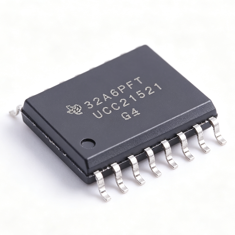
UCC21521DWR - 4A/6A 5.7kVrms Isolated Gate Driver | TI
The Texas Instruments UCC21521DWR is a 4-A source / 6-A sink dual-channel reinforced isolated gate driver with 5.7-kV RMS galvanic isolation, at least 100 V/ns common-mode transient immunity (CMTI), and a 16-pin SOIC (DW) package. An isolated gate driver is a power-management IC that translates low-voltage control logic from a microcontroller or DSP into the high peak current required to switch power transistors, while maintaining galvanic isolation between the control side and the power stage. Within the power-electronics hierarchy it sits between PWM controllers and MOSFETs, IGBTs, or SiC MOSFETs, and it is essential for safety isolation and noise immunity in high-voltage converters. Key features include 19-ns typical propagation delay, 5-ns maximum channel-to-channel matching, 6-ns maximum pulse-width distortion, and a 10-ns minimum input pulse width. These tight timing specifications reduce switching losses and minimize shoot-through risk. The DIS enable pin supports power sequencing and fast fault shutdown, and programmable dead time (for half-bridge configurations) prevents cross-conduction. Technically, the UCC21521 uses TI capacitive isolation technology to deliver the 5.7-kV RMS reinforced barrier with CMTI of at least 100 V/ns, making it robust in high dv/dt SiC environments. Input thresholds are TTL and CMOS compatible for direct 3.3-V logic interfacing, and an 8-V UVLO protects the power switch from under-driven operation. Typical applications include motor drives, solar string inverters, EV onboard chargers, and isolated DC-DC converters, where the 4-A/6-A drive strength and up-to-5-MHz switching capability suit SiC and IGBT power stages. Design tip: place decoupling capacitors directly at VCCI and VDDA/VDDB pins and minimize gate-loop inductance to achieve the datasheet timing figures and avoid dv/dt-induced false triggering. This page adds value beyond the datasheet with drop-in alternative comparisons, pricing tiers, and practical layout notes synthesized from distributor and manufacturer data.
UCC21521Q-Q1 - 4A/6A 5.7kVRMS Dual Gate Driver | Texas Instruments
The Texas Instruments UCC21521Q-Q1 is an AEC-Q100 qualified, 5.7-kVRMS isolated dual-channel gate driver delivering 4-A source and 6-A sink peak output current, housed in a 16-pin SOIC (DW) package. The device is universal in topology, supporting dual low-side, dual high-side, or half-bridge driver configurations, and includes an enable pin for system-level control. An isolated gate driver is a power management IC that provides galvanic isolation between the low-voltage controller side and the high-voltage power stage, allowing a microcontroller to safely drive power semiconductor switches such as MOSFETs, SiC FETs, and IGBTs. Gate drivers form the interface layer of the power-conversion hierarchy: controller -> signal isolator -> gate driver -> power switch. Key features include capacitive-coupled isolation rated at 5700 Vrms, high CMTI (common-mode transient immunity) for fast-switching wide-bandgap applications, a UVLO (undervoltage lockout) on both input and output supplies that prevents erratic gate drive during power-up, and an enable pin that places both outputs low for safety interlocks. The 4-A/6-A asymmetrical drive strength provides strong turn-off capability that minimizes switching losses and improves dv/dt immunity against parasitic turn-on. The Q1 grade guarantees operation from -40C to +125C ambient under AEC-Q100 automotive qualification, making the device suited to traction inverters, on-board chargers, and 48V systems. The universal channel configuration lets a single bill-of-material position cover half-bridge, dual low-side, and dual high-side designs, reducing qualification overhead across platforms. Typical applications include automotive traction inverters, OBC PFC and LLC power stages, DC fast-charger modules, solar string inverters, and industrial motor drives driving SiC or IGBT switches. The wide-body creepage and clearance of the SOIC-16 (DW) package supports reinforced isolation designs. Design consideration: size the gate-loop resistance to balance switching speed against ringing, and place the driver close to the power switch to minimize loop inductance; always verify CMTI margin against the fastest dv/dt in the system. Pricing data as of 2026-08-29; see tiers below for quantity pricing.

UCC21530 - 4A/6A 5.7kVRMS Isolated Dual Gate Driver | TI
The Texas Instruments UCC21530 is an isolated dual-channel gate driver delivering 4A source and 6A sink peak output current in a 14-pin SOIC (DWK) package. It is designed to drive IGBTs, Si MOSFETs, and SiC MOSFETs at switching frequencies up to 5MHz, with a 5.7kVRMS reinforced isolation barrier and a minimum common-mode transient immunity (CMTI) of 125V/ns. An isolated gate driver is a specialized power-management IC that provides galvanic isolation between a low-voltage controller (MCU or PWM controller) and a high-voltage power stage while supplying the peak current required to switch power transistors rapidly. It sits in the power electronics signal chain between the digital controller and the gate of an IGBT or MOSFET. The UCC21530 uses a capacitive isolation architecture, which enables high-speed signal transfer with low power consumption compared with optocoupler-based drivers. Key features include 4A/6A peak output current, 5.7kVRMS reinforced isolation, 125V/ns minimum CMTI, 3.3mm channel-to-channel spacing, an enable pin, and programmable dead time via the DT pin. According to the TI datasheet, the device offers best-in-class propagation delay and low pulse-width distortion, which reduces dead-time losses and enables precise, efficient switching. Undervoltage lockout (UVLO) on both the input and output sides adds system-level robustness. Architecturally, the UCC21530 comprises an input-side controller coupled through a capacitive isolation barrier to two secondary-side drivers. The reinforced barrier supports demanding safety standards, while internal functional isolation between the two outputs allows independent high-side and low-side operation in half-bridge and full-bridge configurations without external isolation components. Typical applications include three-phase motor drives, solar string inverters, EV onboard chargers, UPS systems, and server power supplies. High peak current and low propagation delay minimize switching losses, while high CMTI prevents false gate triggering at rapidly slewing switch nodes in SiC designs. When designing with the UCC21530, minimize gate-loop parasitic inductance, set dead time correctly via the DT pin to prevent shoot-through, and verify UVLO thresholds against your rail-sequencing plan for reliable startup. Pricing as of 2026-08-30 is available from authorized distributors listed in data sources.

UCC21530Q-Q1 - 4A/6A 5.7kVRMS Isolated Gate Driver | TI
The Texas Instruments UCC21530Q-Q1 is an AEC-Q100 qualified, reinforced isolated dual-channel gate driver delivering 4A source and 6A sink peak output current, designed to drive IGBTs, Si MOSFETs, and SiC MOSFETs at switching frequencies up to 5MHz. It comes in a 14-pin SOIC (DWK) package with a 5.7kVRMS reinforced isolation barrier providing 3.3mm channel-to-channel spacing. An isolated gate driver is a power management IC that transfers logic-level PWM control signals across a galvanic isolation barrier to drive the gate of a high-side or low-side power switch floating at high voltage. Within the power-electronics hierarchy (gate driver -> isolated driver IC -> power management IC -> semiconductor), the UCC21530-Q1 occupies the critical interface between a microcontroller such as the TMS320F28004x C2000 family and the power stage. Key features include best-in-class propagation delay and pulse-width distortion, programmable dead time via a single DT pin resistor, a common-mode transient immunity (CMTI) of at least 125V/ns for operation on fast-switching GaN and SiC bridges, and TTL/CMOS-compatible input thresholds independent of the VDDI supply. An enable pin allows global shutdown, and both outputs can be interlocked for half-bridge configurations. The capacitive isolation architecture supports a maximum repetitive peak isolation voltage suitable for 800V-class automotive systems such as on-board chargers and traction inverters, though designers should verify creepage requirements against the 3mm package spacing. Wide VDDI operation on the output side accommodates 5V-to-20V gate-drive rails needed for SiC MOSFETs. Typical applications include automotive traction inverters, 800V on-board chargers (OBC), DC-DC converters, motor drives, and solar inverters. Pairing the driver with SiC MOSFETs such as the LMG3422 GaFET ecosystem or discrete SiC switches yields low-loss, high-frequency power stages. Design tip: size the DT-pin resistor precisely to set dead time, and place a low-ESR decoupling network (1uF plus 100nF) directly at VDDA and VDDB to sustain 4A/6A peak gate currents without droop.
UCC21540 - 4A/6A 5.7kVRMS Isolated Gate Driver | Texas Instruments
The Texas Instruments UCC21540 is a reinforced isolated dual-channel gate driver delivering up to 4-A peak source and 6-A peak sink current to drive power MOSFETs, IGBTs, and GaN transistors. It carries a 5.7-kVRMS galvanic isolation rating, and the DWK package option provides 3.3-mm channel-to-channel spacing for high bus-voltage industrial designs. An isolated gate driver is a specialized IC that provides galvanic isolation between a low-voltage controller and a high-voltage power stage, enabling safe, ground-loop-free switching of power transistors in the power-conversion hierarchy: gate driver -> isolated driver -> power management IC. The UCC21540 belongs to the UCC2154x family within TI's broad isolated gate driver portfolio, optimized for 10-12V driven MOSFETs and IGBTs. Key features include 4-A/6-A peak drive strength, 5.7-kVRMS reinforced isolation per the capacitive isolation technology, a programmable-deadtime (DT) pin that prevents shoot-through in half-bridge configurations, a disable (DIS) pin for system-level fault shutdown, and an 8-V UVLO on the secondary-side supply. VDD on the output side operates from 6.5V to 18V, supporting both dual low-side and half-bridge topologies. Technically, the device uses TI capacitive isolation technology, delivering fast propagation delay, low channel-to-channel matching error, and high common-mode transient immunity (CMTI), which is essential when switching at high frequency across large dv/dt events such as GaN half-bridge transitions. The dual-input configuration accepts both PWM-style inverting/non-inverting inputs for flexible control interfacing. Typical applications include server and telecom power supplies, industrial motor drives, solar string inverters, and EV onboard chargers, where its combination of drive strength, deadtime control, and isolation robustness maximizes converter efficiency and reliability. Design tip: keep the gate-drive loop compact, set the DT pin resistor for the deadtime your switches require, and respect creepage/clearance spacing on the PCB. According to TI, pricing and availability as of 2026-08-30.
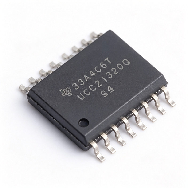
UCC21540QDWKRQ1 - 5.7kVRMS Isolated Dual Gate Driver | Texas Instruments
The Texas Instruments UCC21540QDWKRQ1 is an automotive-grade, AEC-Q100 qualified, reinforced-isolated dual-channel gate driver delivered in a 14-pin SOIC (DWK) package. It provides 4 A peak-source and 6 A peak-sink output current to drive power MOSFET, IGBT, and GaN transistors, with 5700 VRMS galvanic isolation based on capacitive coupling and programmable dead time for half-bridge configurations. An isolated gate driver is a power-management IC that transfers control signals across a galvanic isolation barrier, allowing a controller on the low-voltage side to safely switch power transistors floating at high potential. Isolated gate drivers sit within the broader hierarchy of gate drivers, power management ICs, and semiconductors, and are essential building blocks in any switched-mode power conversion system where the switch node is referenced to a high-voltage rail. Key features include 5700 VRMS reinforced isolation, 8-V UVLO on the secondary side, configurable dual inputs allowing the device to operate as two low-side drivers, two high-side drivers, or a half-bridge driver with independent or interlocked control, and programmable dead time implemented via a single external resistor. The DWK package offers 3.3-mm minimum channel-to-channel spacing for reinforced isolation and a wide operating temperature range suited to automotive under-hood environments. Architecturally, the device uses TI capacitive isolation technology, which provides faster and more consistent propagation delay than optocoupler-based drivers, along with robust common-mode transient immunity. Consistent performance under extreme temperature conditions makes the -Q1 variant suitable for traction inverters, onboard chargers, and other automotive power systems. Typical applications include EV traction inverter half-bridges driving IGBT or SiC/GaN modules, onboard charger and DC-DC converter power stages, solar string inverters, and industrial motor drives. The 4 A/6 A drive strength is well matched to medium-power switches requiring fast turn-off to minimize switching losses. Design tip: size the dead-time resistor precisely and place a low-ESR decoupling capacitor directly across VDDA/VSSA and VDDB/VSSB; verify that the CMTI rating covers the expected dV/dt of your switch node to prevent spurious output transitions.
UCC21550 - 4A/6A 5kVrms Isolated Dual Gate Driver | TI
The Texas Instruments UCC21550 is a reinforced isolated dual-channel gate driver delivering 4A peak-source and 6A peak-sink current to drive power MOSFETs, SiC, GaN, and IGBT transistors. Housed in a 16-pin SOIC (DW) package, it provides 5000Vrms reinforced isolation per UL1577 and operates across a wide -40C to +150C temperature range. The device can be configured as two low-side drivers, two high-side drivers, or a half-bridge driver. An isolated gate driver is an integrated circuit that supplies the gate charge current needed to switch power transistors while maintaining galvanic isolation between the low-voltage controller and the high-voltage power stage. Within the power management hierarchy (gate driver -> isolated gate driver -> power management IC), isolation is critical for safety, noise immunity, and level-shifting in high-voltage systems such as motor drives and solar inverters. Key features include the high 4A/6A peak currents that rapidly charge and discharge large gate capacitances, reducing switching losses in SiC and GaN converters. Programmable dead time, set by a resistor on the DT pin, prevents shoot-through in half-bridge topologies. Capacitive silicon-dioxide isolation technology provides high common-mode transient immunity (CMTI), essential when switching fast SiC devices at high dv/dt. Undervoltage lockout (UVLO) on both input and output supplies protects against brownout conditions, and the family offers multiple UVLO and dead-time grade options (A/B/C variants). Technically, the UCC21550 transfers PWM signals across a capacitive isolation barrier with low propagation delay and tight channel-to-channel matching, according to TI datasheet UCC21550 (46 pages). Typical applications include switch-mode power supplies, solar string inverters, motor drives, EV onboard chargers, and industrial power conversion. The wide temperature range and reinforced isolation suit automotive and industrial environments (an AEC-Q100 qualified UCC21550x-Q1 family is available). Design tip: place the driver close to the power transistors to minimize gate-loop parasitic inductance, and size the DT resistor dead time to the switching characteristics of the connected transistors to prevent shoot-through.
UCC21550ADWR - 4A/6A Isolated Dual Gate Driver | Texas Instruments
The Texas Instruments UCC21550ADWR is a 5000Vrms reinforced-isolated dual-channel gate driver with 4A peak source and 6A peak sink output current, programmable dead time, and CMTI greater than 125 V/ns, housed in a 16-pin SOIC (DW) package. An isolated gate driver is a power management IC that translates low-voltage logic signals across a galvanic isolation barrier to drive the gate of a power transistor such as a MOSFET, SiC MOSFET, GaN FET, or IGBT. Within the power-conversion hierarchy, it sits between the PWM controller or microcontroller and the power stage, providing both the current amplification needed to switch power devices quickly and the isolation needed to shift logic references to high-side or floating switch nodes safely. Key features include configurable operation as two low-side drivers, two high-side drivers, or a half-bridge driver; a wide VDD output supply range up to 25V; a 5V undervoltage lockout (UVLO) option; and an integrated DISABLE pin for immediate output control. The capacitive-coupling isolation architecture delivers high common-mode transient immunity, critical for SiC and GaN converters whose fast switching edges (dV/dt exceeding 100 V/ns) would corrupt optocoupler-based drivers. Technically, the UCC21550 uses TI capacitive isolation technology with on-chip logic that supports programmable dead time via an external resistor, protecting half-bridge power stages from shoot-through. The asymmetric 4A source / 6A sink capability turns off power devices faster than it turns them on, minimizing switching losses and reducing the risk of parasitic turn-on in bridge topologies. The junction temperature range of -40C to +150C supports demanding thermal environments such as automotive traction inverters and industrial drives. Typical applications include solar inverters, motor drives, onboard chargers, server and telecom power supplies, and SiC/GaN half-bridge power stages where high CMTI and fast propagation are essential. The device suits engineers consolidating on one driver family across MOSFET, IGBT, SiC, and GaN platforms. A key design consideration: verify the 5V UVLO threshold matches your gate-drive supply - for SiC MOSFETs requiring 15V-to-18V drive, confirm UVLO behavior remains valid across the full 25V VDD range, and always place a low-ESR ceramic capacitor close to VDD. This page adds value beyond the manufacturer datasheet by combining distributor pricing, verified drop-in alternatives within the same family, engineering design notes, and application-level selection guidance in one place.
UCC21550AQDWKRQ1 - 4A/6A 5kVRMS Isolated Gate Driver | TI
The Texas Instruments UCC21550AQDWKRQ1 is an automotive-grade, reinforced isolated dual-channel gate driver delivering 4 A peak source and 6 A peak sink current, with 5000 Vrms galvanic isolation based on capacitive coupling, housed in a 14-pin SOIC (DWK) package. Per the TI UCC21550-Q1 datasheet, the device integrates a dedicated DIS (disable) pin and a DT (dead time) pin for programmable dead-time control. An isolated gate driver is a power management IC that transfers logic-level PWM control signals across a galvanic isolation barrier to drive the gate of a power semiconductor operating at high voltage. In the power-electronics hierarchy, it sits between the PWM controller or MCU and the power stage (MOSFET, SiC MOSFET, GaN FET, or IGBT), providing both safety isolation and the high peak current needed to switch power devices quickly and efficiently. Key features include the 4 A/6 A asymmetric drive strength that accelerates turn-off to reduce switching losses, 5 kVRMS reinforced isolation suitable for high-voltage industrial and automotive buses, and programmable dead time via a single resistor on the DT pin, which simplifies half-bridge design and protects against shoot-through. The DIS pin allows immediate output disable for fault handling. Architecturally, the input side (INA, INB, DIS) uses TTL- and CMOS-compatible input thresholds isolated from the VDD supply. The UCC21550-Q1 can be configured as two low-side drivers, two high-side drivers, or a half-bridge driver, giving designers one part number for multiple topologies. Capacitive isolation technology provides high CMTI and long-term barrier reliability for automotive environments. Typical applications include onboard chargers (OBC), traction inverters, and DC-DC converters in electric vehicles, as well as solar inverters, motor drives, and server/telecom power supplies where SiC or IGBT switches demand robust, isolated gate drive. Design-wise, use the DT pin resistor to set dead time per your switch technology; SiC and GaN typically need shorter dead time than IGBTs. Ensure VDD decoupling with low-ESR ceramics close to the driver. This page synthesizes distributor pricing, drop-in family alternatives, and practical design notes not found in the manufacturer datasheet.
UCC21550BDWR - 4A/6A Dual Isolated Gate Driver | Texas Instruments
The Texas Instruments UCC21550BDWR is a reinforced isolated dual-channel gate driver delivering 4 A peak source and 6 A peak sink output current, with 5000 Vrms galvanic isolation and common-mode transient immunity (CMTI) greater than 125 V/ns, housed in a 16-pin SOIC (DW) package. An isolated gate driver is a power-management IC that transfers a logic-level PWM signal across a galvanic isolation barrier to drive the gate of a power transistor such as a MOSFET, SiC MOSFET, GaN FET, or IGBT sitting on a high-voltage or floating potential. It sits in the signal chain between the PWM controller or microcontroller and the power stage, forming the critical interface in any isolated power conversion system. Key features include universal configuration as two low-side drivers, two high-side drivers, or one half-bridge driver; programmable dead time for shoot-through protection; a disable function; VDD output supply up to 25 V for direct drive of wide-bandgap devices; and a junction temperature range of -40 C to +150 C for demanding thermal environments. The capacitive coupling isolation technology provides a minimum isolation withstand of 5000 Vrms. Architecturally, the input side is isolated from the two output drivers by a silicon-dioxide capacitive isolation barrier, which rejects the extremely fast dv/dt transients generated by SiC and GaN power stages. The 8 V UVLO threshold ensures outputs are held low until the driver supply is stable, preventing half-bridge shoot-through during startup. Typical applications include solar inverters, motor drives, server and telecom power supplies, on-board chargers, and industrial half-bridge power stages using SiC or IGBT switches. Design-wise, place a low-ESR decoupling capacitor close to VDD/VSS on both sides of the barrier, and use the programmable dead-time pins to match the switching characteristics of the selected power transistor. This page synthesizes distributor pricing, drop-in alternatives, and practical design notes not found in the manufacturer datasheet.
UCC21550BQDWRQ1 - 4A/6A Automotive Isolated Gate Driver | Texas Instruments
The Texas Instruments UCC21550BQDWRQ1 is an automotive-grade (AEC-Q100 qualified, UCC21550-Q1 family) reinforced-isolated dual-channel gate driver delivering 4A peak source and 6A peak sink output current, with 5000Vrms galvanic isolation via on-chip capacitive coupling, packaged in a 16-pin SOIC (DW) surface-mount package. An isolated gate driver is a power-management IC that translates low-voltage PWM logic signals across a galvanic isolation barrier to drive the gate of a power transistor floating at high voltage. Within the power electronics hierarchy, it sits between the PWM controller or MCU (such as a C2000 DSP) and the power switch (MOSFET, SiC MOSFET, GaN FET, or IGBT), and is fundamental to isolated half-bridge, full-bridge, and boost converter stages in industrial and automotive power systems. Key features of the UCC21550BQDWRQ1 include programmable dead time via an external resistor, a disable pin for fast shutdown, 8V undervoltage lockout (UVLO) on the driver supply for robust SiC/IGBT gate protection, and flexible configuration as two low-side drivers, two high-side drivers, or one half-bridge driver. The reinforced isolation barrier supports functional safety and high-voltage designs per automotive requirements. Architecturally, the device uses TI capacitive isolation technology, which provides high common-mode transient immunity and fast, precise signal transfer across the barrier. The wide operating temperature range supports underhood and industrial environments, and the 4A/6A asymmetric drive strength allows fast turn-off to minimize switching losses in SiC and IGBT stages. Typical applications include onboard chargers, DC-DC converters, traction inverters, solar string inverters, and motor drives, where a floating high-side switch and reinforced isolation are mandatory. Design consideration: select the dead-time resistor value per the datasheet formula and verify the driver-side UVLO threshold (8V) matches the selected SiC MOSFET gate-plateau requirements to avoid operating the switch in a high-resistance region. This page synthesizes distributor availability data, TI product pages, drop-in family alternatives, and practical design notes not consolidated in the manufacturer datasheet alone.
UCC21550Q-Q1 - 4A/6A Isolated Dual Gate Driver | TI
The Texas Instruments UCC21550Q-Q1 belongs to the UCC21550-Q1 automotive family of reinforced isolated dual-channel gate drivers with programmable dead time, delivering 4A peak-source and 6A peak-sink output current to drive power MOSFET, SiC, GaN, and IGBT transistors. It is offered in a 16-pin SOIC (DW) package rated at 5000Vrms reinforced isolation and an operating temperature range of -40C to 150C. An isolated gate driver is a power management IC that provides galvanic isolation between a low-voltage controller (such as an MCU) and the high-voltage power stage of a switching converter or motor inverter. Within the power-electronics hierarchy, it sits between the PWM controller and the power transistor, translating logic-level signals across the isolation barrier while providing the high peak currents needed to rapidly charge and discharge transistor gates. Key features include a capacitive isolation architecture with high common-mode transient immunity for fast-switching WBG devices, programmable dead time via a single resistor for half-bridge configurations, and flexible configuration as two low-side, two high-side, or one half-bridge driver. A disable pin and interlock function prevent shoot-through. Per TI product data, the family supports both A and B grade options with different propagation delay specifications. The driver uses TI capacitor-based isolation technology, which avoids the aging characteristics of optocouplers and sustains high dV/dt events typical of SiC and GaN switching. High CMTI and fast propagation delay enable narrow dead times, improving converter efficiency in high-frequency designs. Typical applications include on-board chargers and traction inverters in electric vehicles, solar string inverters, industrial motor drives, server and telecom power supplies, and wireless charging power stages. Design consideration: program the dead-time resistor per the datasheet equation and keep the gate-drive loops short; verify thermal dissipation from gate-charge losses at your switching frequency before finalizing the layout.
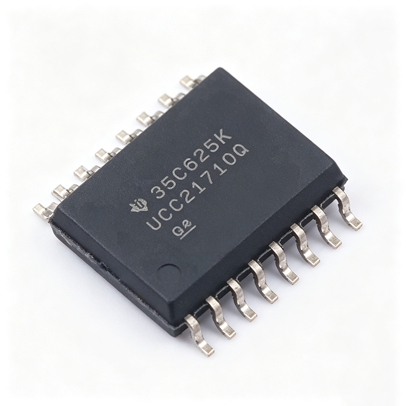
UCC21710-Q1 - 10A Isolated Gate Driver | Texas Instruments
The Texas Instruments UCC21710-Q1 is a galvanic isolated single-channel gate driver designed for high-power SiC MOSFETs and IGBTs up to 1700 V. It delivers up to ±10 A peak source and sink current in a 16-SOIC package, enabling fast switching of large power modules. The driver integrates reinforced isolation rated at 5700 Vrms, with high common-mode transient immunity (CMTI) for robust operation in noisy environments. A gate driver is a power-management IC that converts low-voltage control signals from a microcontroller into high-current pulses to drive the gate of power transistors. In a system hierarchy, the gate driver sits between the controller and the power switch, providing isolation and signal amplification. The UCC21710-Q1 belongs to the isolated gate driver family, which adds galvanic isolation to protect low-voltage control circuitry from high-voltage transients. Key features include: ±10 A peak source/sink current, 5700 Vrms reinforced isolation, single-channel operation, and input and output side UVLO. It supports overcurrent (OC) and short-circuit detection via shunt sensing, active Miller clamp to prevent spurious turn-on, fault reporting, and isolated analog-to-PWM sensing for temperature or voltage monitoring. These features provide comprehensive protection for SiC and IGBT switching. The UCC21710-Q1 uses capacitive coupling for signal transfer, achieving high CMTI. It is AEC-Q100 qualified for automotive applications, meeting the reliability demands of HEV/EV traction inverters. The device's short-circuit clamping feature limits gate voltage to slightly above VDD, protecting semiconductors from gate-source/emitter overvoltage breakdown. Typical applications include HEV/EV traction inverters, solar inverters, industrial motor drives, UPS, wind turbine converters, and railway traction. The high peak current and 1700-V rating allow it to directly drive large IGBT modules and SiC MOSFETs without external buffers. Its isolation enables safe operation in high-voltage DC-link systems. When designing with this device, ensure proper bias supplies: UCC14240-Q1 is a recommended isolated power supply for the output side. Pay attention to gate loop inductance and maintain adequate PCB spacing for reinforced isolation. The active Miller clamp must be connected to the gate to prevent high dV/dt-induced turn-on.
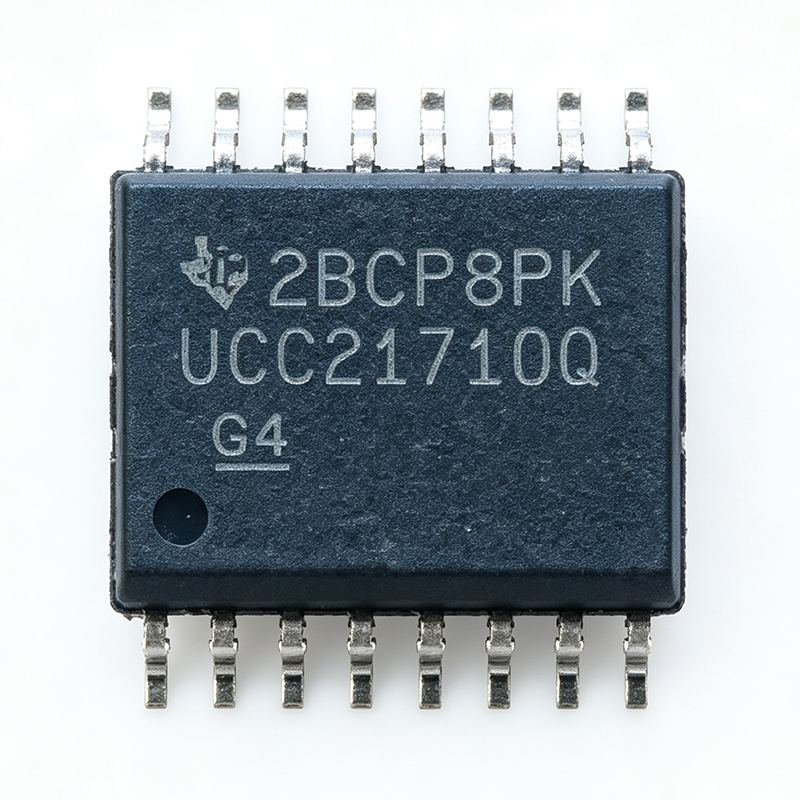
UCC21710QDWRQ1 - 10A Isolated Gate Driver | TI | Automotive
The UCC21710QDWRQ1 from Texas Instruments is an automotive-grade, galvanically isolated single-channel gate driver designed for up to 1700V SiC MOSFETs and IGBTs. It delivers ±10A peak source and sink current, with a 5.7kVrms isolation rating and high common-mode transient immunity (CMTI) for robust performance in noisy power environments. The device is housed in a 16-pin SOIC (DW) package and is AEC-Q100 qualified for automotive applications. A gate driver is a power amplifier that accepts a low-power input from a controller IC and produces a high-current drive output to efficiently switch power transistors such as IGBTs and SiC MOSFETs. In the hierarchy of power electronics, a gate driver sits between the control stage (microcontroller/DSP) and the power stage (switching devices), forming a critical link in the signal chain. Isolated gate drivers add galvanic isolation to protect low-voltage control circuitry from high-voltage transients and ground loops, which is essential in motor drives, inverters, and power supplies. Key features include fast overcurrent and short-circuit protection with shunt current sensing, fault reporting, active Miller clamp, and input/output side power supply UVLO. The isolated analog-to-PWM sensor enables easy temperature or voltage sensing across the isolation barrier. The device supports up to 1.5kVrms working voltage and 12.8V to 18V output supply range, with a typical propagation delay of 60ns and CMTI of 100V/ns. The UCC21710-Q1 uses SiO2 capacitive isolation technology, providing reliable isolation and high-speed signal transfer. Its advanced protection features optimize SiC and IGBT switching behavior, reducing switching losses and enhancing system robustness. The active Miller clamp prevents false turn-on during high dv/dt events, while the fast fault response (within 100ns) protects the power stage from damage. Typical applications include traction inverters in electric vehicles, on-board chargers, DC-DC converters, motor drives, and industrial power supplies. The automotive qualification and wide temperature range (-40°C to +150°C) make it suitable for under-hood and high-temperature environments. When designing with this device, ensure proper PCB layout with short, low-inductance gate drive loops and adequate creepage/clearance for the isolation rating. The DESAT protection requires an external diode and resistor network to sense collector-emitter voltage, and the shunt current sensing input should be filtered to avoid false triggering.

UCC27511A - 4A/8A Low-Side Gate Driver | Texas Instruments
The Texas Instruments UCC27511A is a single-channel, high-speed low-side gate driver designed to drive MOSFETs, IGBTs, and emerging wide bandgap power devices such as GaN. It delivers 4-A peak source and 8-A peak sink currents, with a propagation delay of only 13 ns, making it suitable for high-frequency switching applications. The device operates from a 4.5-V to 18-V supply and features split outputs (OUTH and OUTL) for independent turn-on and turn-off control, as well as an enable pin with 5-V input handling capability. A low-side gate driver is a type of power management IC that amplifies control signals from a controller to efficiently switch a ground-referenced power transistor. It sits between the PWM controller and the gate of a MOSFET or IGBT, providing the high peak currents needed to charge and discharge the gate capacitance quickly. This reduces switching losses and improves efficiency in power converters. The UCC27511A belongs to the gate driver family, which is a subset of power management ICs essential for modern power electronics. Key features include a 13-ns propagation delay, 4-A source and 8-A sink peak currents, and a 5-V UVLO (undervoltage lockout) with hysteresis. The split outputs allow independent control of rise and fall times, enabling designers to optimize switching performance and reduce EMI. The device also features a robust design that minimizes shoot-through current, enhancing reliability in noisy environments. Technically, the UCC27511A uses a CMOS-based architecture that provides rail-to-rail output swing and high noise immunity. The input stage can handle 5-V logic signals directly, simplifying interface with microcontrollers and PWM controllers. The device is available in a SOT-23-6 package, which is compact and suitable for space-constrained designs. Typical applications include switch-mode power supplies, DC-to-DC converters, and companion gate-driver circuits for power modules. Its high-speed performance makes it ideal for synchronous rectification, active clamping, and other high-frequency topologies. When designing with the UCC27511A, ensure proper decoupling of the VDD pin with a 1-uF ceramic capacitor placed close to the device. The split outputs allow tuning of gate drive strength; use separate resistors on OUTH and OUTL to adjust rise and fall times independently.