Clock & Timing
ژێرپۆلەکان
بەرهەمەکان (32)

AD9901TQ/883B - 200MHz Phase/Frequency Discriminator | Analog Devices
The AD9901TQ/883B is a military-grade, ultrahigh-speed phase/frequency discriminator from Analog Devices, designed for phase-locked loop (PLL) applications requiring precise frequency and phase comparison up to 200 MHz. Housed in a 14-pin ceramic dual-in-line package (CDIP) with a 0.300-inch body width, this through-hole component operates over the full military temperature range of -55°C to +125°C and is compliant with MIL-STD-883 standards, ensuring reliability in harsh environments. A phase/frequency discriminator is a critical building block in PLL systems, comparing the phase and frequency of an input signal against a reference and producing an error output that drives the loop filter and VCO to achieve lock. Unlike a simple phase detector, it provides both phase and frequency discrimination, enabling faster lock acquisition and wider capture range. In the hierarchy of clock and timing ICs, it falls under phase-locked loops, which are essential for frequency synthesis, clock recovery, and signal conditioning in communication and instrumentation systems. Key features of the AD9901TQ/883B include its 200 MHz maximum input frequency, which supports high-speed PLL designs, and its digital output that interfaces directly with charge pumps or loop filters. The device operates from a single 5V supply, simplifying power design, and its ceramic package offers superior thermal and mechanical stability compared to plastic packages, making it suitable for military and aerospace applications. The MIL-STD-883 compliance ensures rigorous testing and quality assurance, including hermeticity and temperature cycling. Technically, the AD9901 employs a digital phase/frequency detector architecture that provides a tri-state output, minimizing dead zone and reducing spurious signals in the PLL. Its high-speed operation is achieved through advanced bipolar process technology, delivering fast propagation delays essential for high-frequency loops. The device's input sensitivity and wide bandwidth make it versatile for various reference frequencies, from low-frequency crystal oscillators to high-frequency VCO outputs. Typical applications include frequency synthesizers in radar and communication systems, phase-locked oscillators for satellite communications, and clock recovery circuits in high-speed data links. Its military-grade qualification makes it ideal for avionics, defense electronics, and space systems where reliability is paramount. When designing with this device, ensure proper decoupling of the 5V supply with 0.1uF ceramic capacitors close to the VCC pin, and consider the output loading to avoid excessive current draw. The ceramic DIP package requires through-hole soldering, and thermal management is generally not a concern due to low power dissipation, but adequate ground plane is recommended for noise immunity.
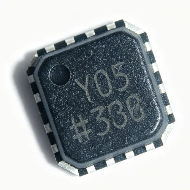
ADCLK905 - Ultrafast SiGe ECL Clock/Data Buffer | Analog Devices
The ADCLK905 is an ultrafast clock/data buffer fabricated on Analog Devices' proprietary XFCB3 silicon germanium (SiGe) bipolar process. It features one input and one output, with full-swing emitter coupled logic (ECL) output drivers. Key specifications include a 95 ps propagation delay, 7.5 GHz toggle rate, 60 ps typical output rise/fall time, and 60 fs random jitter (RJ). The device operates over an extended industrial temperature range and includes on-chip terminations at both input pins. It is available in a 16-lead LFCSP (VQFN) package with exposed pad, suitable for high-speed signal distribution in test and measurement, communications, and data acquisition systems. A clock/data buffer is a high-speed integrated circuit that receives a clock or data signal and re-drives it to one or more outputs with minimal added jitter and propagation delay. It is a critical component in signal distribution networks, ensuring signal integrity across multiple loads. The ADCLK905 belongs to the category of clock buffers, which are part of the broader clock and timing IC family. These devices are essential in systems where precise timing and low jitter are paramount, such as in high-speed ADCs, DACs, and serial data links. Key features of the ADCLK905 include its 7.5 GHz toggle rate, which enables distribution of very high-frequency clocks, and its 60 fs random jitter, which preserves signal integrity in demanding applications. The 95 ps propagation delay ensures minimal latency, and the on-chip terminations simplify PCB layout by reducing external component count. The ECL output drivers provide full-swing signals compatible with ECL logic levels, and the extended industrial temperature range (-40°C to +125°C) supports harsh environments. Technically, the ADCLK905 leverages the XFCB3 SiGe bipolar process, which offers high-speed performance with low power consumption. The device includes a differential input and output, allowing for flexible signal routing. The on-chip terminations at both input pins reduce reflections and improve signal quality. The LFCSP package with exposed pad provides excellent thermal performance, enabling reliable operation at high frequencies. Typical applications include clock distribution for high-speed ADCs and DACs, data buffering in serial communication links, and signal conditioning in test and measurement equipment. The ADCLK905 is also suitable for use in RF and microwave systems where low jitter and high toggle rates are critical. When designing with the ADCLK905, it is important to use high-quality PCB materials and proper termination techniques to maintain signal integrity at multi-gigahertz frequencies. The evaluation board uses high-quality dielectric material between layers to ensure optimal performance.

ADF4154BCPZ-RL7 - 4 GHz Fractional-N PLL Synthesizer | Analog Devices
The Analog Devices ADF4154BCPZ-RL7 is a fractional-N frequency synthesizer for RF local-oscillator generation, with an RF input bandwidth up to 4 GHz, dual-modulus prescalers of 4/5 and 8/9, and a 3-wire serial programming interface. It is supplied in a 20-lead WFQFN exposed-pad chip-scale package for compact RF and microwave signal-chain designs. A fractional-N frequency synthesizer is a phase-locked-loop device that generates precise local-oscillator signals for RF transmitters and receivers. The ADF4154 combines a low-noise digital phase-frequency detector, a precision charge pump, a programmable reference divider, and a sigma-delta fractional interpolator. This architecture supports integer and fractional division ratios while preserving stable phase locking across programmable output frequencies. The principal operating features include RF bandwidth to 4 GHz, a 2.7 V to 3.3 V power supply, programmable charge-pump currents, a separate VP tuning-voltage supply, digital lock detection, and power-down mode. The dual 4/5 and 8/9 prescalers extend the usable integer-N range, while the sigma-delta fractional interpolator enables fine frequency synthesis for wireless transceiver architectures. The 3-wire serial interface provides a compact control path for programming divider ratios, prescaler selection, charge-pump settings, and power state. The device is designed for direct PCB integration where RF routing, grounding, decoupling, and exposed-pad thermal management are critical. Its separate VP connection allows the tuning-voltage range to be extended beyond the constraints imposed by the main supply when appropriate external circuitry and voltage limits are used. Typical applications include wireless receiver and transmitter local oscillators, microwave up-converters and down-converters, frequency-agile test equipment, RF signal generators, radar-related signal chains, and industrial RF communication systems. In these systems, the synthesizer supplies a programmable reference for mixers or other RF conversion stages. PCB design should minimize RF trace loss, maintain a continuous ground reference beneath the exposed pad, and place supply and decoupling connections close to their associated pins. Loop-filter components and the reference input should be positioned to avoid noisy digital-control coupling. The manufacturer datasheet is the controlling reference for register programming, pin assignments, recommended application circuits, and absolute operating limits. This product page consolidates the verified device identity, package information, manufacturer documentation, operating features, sourcing guidance, and practical integration considerations. It also distinguishes true pin-compatible family alternatives from parts that require different packages or different synthesizer architectures, helping engineers evaluate replacement options without implying that every similar PLL is a drop-in replacement.

ADF4360-2BCP - 2 GHz Integer-N VCO | Analog Devices
Analog Devices ADF4360-2BCP is a fully integrated integer-N synthesizer and voltage-controlled oscillator with a 2000 MHz center frequency, 3.6 V power supply, 1.8 V logic compatibility, and a 24-lead LFCSP exposed-pad package. Its integrated VCO and synthesizer architecture provides RF outputs around 2 GHz, while a divide-by-2 mode produces an RF output from 925 MHz to 1085 MHz. The device uses a 3-wire serial interface for register control and includes programmable output power, digital lock detection, and hardware and software power-down functions. An integer-N frequency synthesizer is a clock-generation and phase-locking category that combines a frequency divider, phase detector, charge pump, loop filter, and voltage-controlled oscillator. The integer-N architecture provides direct frequency synthesis from a stable reference source, allowing an external reference and feedback divider to establish the desired output relationship. In a wireless receiver, transmitter, test instrument, or frequency-conversion block, this hierarchy operates as a clock generator, then a phase-locked loop, and ultimately an RF frequency synthesizer and power-management supporting semiconductor. The ADF4360-2 family integrates the VCO and most synthesizer functions into one component, reducing board area and external assembly compared with a discrete oscillator and divider arrangement. Programmable output power provides an adjustment range for downstream circuitry. Digital lock detection lets a host controller monitor loop-lock status, while hardware and software power-down modes support systems that need to reduce consumption or control sequencing. The 3.6 V supply and 1.8 V-compatible serial interface support integration with modern controller logic. The divide-by-2 option broadens the usable output range by translating the approximately 2 GHz synthesizer signal into a 925 MHz to 1085 MHz RF output. This capability is useful when a downstream receiver, mixer, or measurement chain requires frequencies below the fundamental VCO range. Integer-N synthesis also makes channel selection programmable, although reference-divider, feedback-divider, loop-filter, and output-buffer settings determine phase noise, tuning range, lock behavior, and spur performance in the completed design. Typical applications include wireless local-area network transceiver frequency generation, cellular and microwave communication equipment, RF test and measurement instruments, frequency-conversion stages, and clocking or modulation subsystems in industrial electronics. In these systems, the device can derive coherent RF or baseband-related clocks from a shared reference while the integrated lock detector reports operating status to the controller. The principal design trade-off is that a compact integrated synthesizer does not remove the need for careful support-circuit and layout work. Reference routing, supply decoupling, the loop filter, VCO output matching, exposed-pad thermal management, and RF return paths can materially affect lock performance and phase noise. Follow the pin-description and application information in the Analog Devices datasheet when assigning tracks and selecting component values. This page combines the device architecture, package details, drop-in family alternatives, and application-focused design guidance to support faster component selection. It also distinguishes the fundamentals from the divide-by-2 operating range, helping engineers identify the correct ADF4360 center-frequency option before beginning PCB implementation.
ADF4360-8BCPRL - 65-400 MHz Integer-N VCO | Analog Devices
The Analog Devices ADF4360-8BCPRL is an integrated integer-N frequency synthesizer and voltage-controlled oscillator covering 65 MHz to 400 MHz, powered from a 3.6 V supply and housed in a 24-lead LFCSP-24 package with an exposed pad. It combines a programmable PLL, integer-N frequency divider, and VCO in one 4 x 4 mm surface-mount device. An integer-N frequency synthesizer is a phase-locked-loop-based clock and RF signal generator that produces an output frequency selected through integer division of a reference clock. The ADF4360-8 belongs to the frequency synthesizer, clock generator, and RF signal-chain hierarchy. Its external-inductor VCO core allows the center frequency to be established with external components rather than a fixed on-chip resonator. The device operates from 3 V to 3.6 V and supports 1.8 V-compatible serial-interface logic. Key features include programmable output power, a three-wire serial interface, digital lock detect, and hardware and software power-down modes. These controls support orderly clock management in RF test equipment, cellular infrastructure, telemetry systems, and other frequency-generation equipment. The integrated architecture reduces the number of external frequency-generation components while retaining direct digital control of the synthesizer. External inductors determine the 65 MHz to 400 MHz operating band, while the integer-N divider establishes the output relationship to the reference frequency. The exposed thermal pad provides the primary heat-spreading path from the 24-lead LFCSP package. Typical uses include cellular baseband and RF test systems, local oscillator generation, wireless transceiver subsystems, and instrumentation requiring programmable RF outputs. The device is particularly suitable where a compact synthesizer with an integrated VCO is preferable to a PLL and separate VCO assembly. Use the manufacturer pin-description table when assigning PCB tracks, and connect the exposed pad to the appropriate ground-plane structure. Follow the recommended decoupling and external-inductor layout because the PLL/VCO loop can be affected by supply impedance and high-frequency grounding quality.

ADF4372BCCZ-RL7 - 16 GHz Integer-N PLL Synthesizer | Analog Devices
Analog Devices ADF4372BCCZ-RL7 is an integer-N phase-locked-loop frequency synthesizer with an integrated voltage-controlled oscillator, a maximum output frequency of 16 GHz, and a 48-lead TFLGA package with an exposed pad. Its VCO fundamental range extends from 4 GHz to 8 GHz, while programmable RF outputs cover 62.5 MHz to 16 GHz. A phase-locked loop, or PLL, synchronizes an output oscillator to a stable reference frequency. The ADF4372 integrates the VCO and synthesizer circuitry into one RF device, allowing a reference oscillator and external loop filter to define a phase-locked output. Its integer-N architecture avoids the fractional-N spur and phase-noise behavior associated with fractional dividers, making it suitable for coherent RF systems requiring predictable spectral content. The device supports RF division by 1, 2, 4, 8, 16, 32, or 64. This allows the 4 GHz to 8 GHz VCO fundamental to be divided down to outputs as low as 62.5 MHz at RF8x. A frequency multiplier provides an 8 GHz to 16 GHz range at RF16x, and RFAUX8x provides an auxiliary output at the eighth-divider frequency. As an integer-N synthesizer, the ADF4372 provides a single programmable output path rather than independent fractional and integer divider systems. The implementation requires an external reference and loop filter. Loop-filter component values determine reference-to-output multiplication ratio, bandwidth, phase noise, and transient behavior, so the reference frequency and target channel spacing must be considered together during design. Typical applications include microwave and millimeter-wave radio front ends, instrumentation, test and measurement equipment, radar-related signal generation, and wideband communication modules. The 16 GHz maximum output supports Ku-band and related RF systems, while the broad divided-output range allows the same synthesizer to support lower-frequency receiver and test circuits. PCB implementation requires careful treatment of the exposed thermal pad, supply connections, RF outputs, and high-speed reference signals. The exposed pad must be connected to the ground plane with adequate thermal-via density, and the external loop filter should be positioned to minimize sensitive RF and feedback-trace coupling. This page combines the ADF4372 frequency ranges, output architecture, package information, sourcing guidance, replacement considerations, and practical PCB-design guidance into a compact engineering reference for evaluating the ADF4372BCCZ-RL7 in integer-N RF synthesizer designs.
ADF5610BCCZ-RL7 - 14.6 GHz Integrated VCO PLL | Analog Devices
The Analog Devices ADF5610BCCZ-RL7 is a microwave wideband frequency synthesizer with an integrated voltage-controlled oscillator, supporting integer-N and fractional-N phase-locked-loop operation up to 14.6 GHz in a 48-VFLGA exposed-pad package. It is designed for RF and microwave systems that require an integrated synthesizer, flexible division, and programmable RF output generation. An integrated VCO is a frequency-control component that combines a voltage-controlled oscillator with active frequency-generation circuitry. In the ADF5610, the VCO has a fundamental frequency range of 3650 MHz to 7300 MHz. The fundamental signal is internally doubled and routed to the RFOUT pin, while a differential output provides additional divided frequencies. This architecture places the synthesizer between RF signal-generation functions and wider communications, test, and instrumentation systems. The ADF5610 supports a broad tuning range from approximately 57 MHz at the lowest divided output to 14.6 GHz at the highest output. Its 3-wire serial interface provides programming access for configuration and control. The device is suitable for wideband microwave synthesizer implementations where integrating the VCO into the synthesizer simplifies the RF signal chain and reduces the number of separate frequency-generation components. The core operating principle is fractional-N or integer-N PLL synthesis using an external loop filter and external reference source. The differential divided output can provide divided VCO frequencies, enabling flexible output planning across wideband systems. The integrated VCO also supports a calibration sequence, with a temperature-related calibration voltage available at VPRST for die-temperature estimation during operation. Typical uses include microwave communications modules, radar and test equipment, frequency-conversion subsystems, and wideband RF signal generators. The 48-VFLGA exposed-pad package is intended for surface-mount assembly and requires careful PCB thermal management and short RF connections. The ADF5610BCCZ-RL7 is marked obsolete by the manufacturer’s distributor listing, so new designs should confirm lifecycle status and consider the current ADF5610 product family options before releasing production quantities.
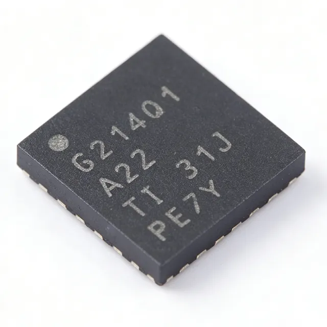
CDCE6214TWRGERQ1 - Ultra-Low Power Clock Generator | TI
The CDCE6214TWRGERQ1 is an automotive-grade, ultra-low power clock generator from Texas Instruments, designed to support PCIe Gen 1-5 with two inputs, four differential outputs, and internal EEPROM. It integrates one fractional-N PLL and can generate five independent clock outputs selectable between various driver modes. The device operates from a 3.3V supply and is packaged in a 24-pin VQFN (4mm x 4mm) with exposed pad, making it suitable for space-constrained automotive and industrial applications. A clock generator is a semiconductor device that produces one or more clock signals from a reference input, typically using a phase-locked loop (PLL) to multiply or divide frequencies. It is a fundamental building block in digital systems, providing timing signals for processors, interfaces, and data converters. Clock generators are part of the broader category of timing and synchronization ICs, which also includes clock buffers, jitter cleaners, and frequency synthesizers. Key features include ultra-low power consumption, medium-grade jitter performance, and a configurable high-performance low-power fractional-N PLL. The device supports I2C-compatible interface up to 400kHz, integrated EEPROM with two pages and an external select pin, and in-situ programming. It also supports 100Ω systems and offers low electromagnetic emissions. The small 24-pin VQFN footprint (4mm x 4mm) enables compact designs. Technically, the CDCE6214-Q1 uses a fractional-N PLL architecture that allows precise frequency synthesis with low spurious content. The RMS jitter with spurs (12kHz - 20MHz, Fout > 100MHz) is specified for integer and fractional modes, ensuring reliable operation in high-speed serial links. The device is AEC-Q100 qualified for automotive applications, meeting stringent reliability and temperature requirements. Typical applications include advanced driver assistance systems (ADAS), automotive infotainment, and industrial automation where multiple clock domains are required. The device can generate clocks for PCIe, Ethernet, and other high-speed interfaces, providing a single-chip solution for clock tree generation. When designing with this device, ensure proper power supply decoupling with 0.1uF and 1uF capacitors close to the VDD pins. The EEPROM can be programmed in-situ via I2C, allowing flexible configuration without external programming hardware. Consider the output driver modes to match the load requirements and minimize signal integrity issues.

CDCLVP110VFR - 1:10 LVPECL/HSTL Clock Driver | Texas Instruments
The Texas Instruments CDCLVP110VFR is a low-voltage 1:10 LVPECL/HSTL to LVPECL clock driver that distributes one differential clock input pair to ten differential LVPECL clock outputs with minimum skew. It operates at frequencies up to 3.5 GHz and is available in a 32-pin LQFP package. The device features a selectable input multiplexer that accepts either LVPECL or HSTL input signals, making it versatile for various high-speed clock distribution applications. A clock driver is an integrated circuit that buffers and distributes clock signals to multiple loads while maintaining signal integrity and minimizing skew. It sits between a clock source, such as an oscillator or PLL, and the downstream components that require synchronized timing. Clock drivers are essential in high-speed digital systems where precise timing is critical, such as data converters, FPGAs, and networking equipment. Key features of the CDCLVP110VFR include a 2:10 configuration (two inputs, ten outputs), support for LVPECL and HSTL input standards, and fully compatible outputs with LVECL/LVPECL/HSTL logic levels. The device operates from a single supply voltage, simplifying power design. It is characterized for operation from -40°C to 85°C, making it suitable for industrial environments. The CDCLVP110VFR uses a differential input structure to reject common-mode noise, ensuring clean clock distribution even in noisy environments. The selectable input multiplexer allows the user to choose between two clock sources, providing redundancy or frequency selection. The outputs are designed to drive 50-ohm transmission lines, and the device includes a VBB reference voltage output for single-ended input operation, though differential mode is recommended for high-speed performance. Typical applications include clock distribution for high-speed ADCs/DACs, FPGA and ASIC clocking, networking switches and routers, and test and measurement equipment. The device's low skew and high frequency capability make it ideal for systems requiring synchronized multi-channel operation. When designing with the CDCLVP110VFR, ensure proper termination of the differential outputs and bypass the power supply pins with decoupling capacitors. For single-ended input, connect the VBB pin to CLK0 with a 10-nF bypass capacitor to ground. For optimal performance up to 3.5 GHz, use differential mode.

CDCM6208VFRGZR - 2:8 Low Jitter Clock Generator | TI
The Texas Instruments CDCM6208VFRGZR is a 2:8 ultra-low power, low jitter clock generator and jitter cleaner with fractional dividers. It provides eight differential or single-ended outputs from two reference inputs, supporting output frequencies up to 800 MHz. The device is housed in a 48-pin VQFN (RGZ) package with an exposed thermal pad, enabling compact board designs. A clock generator is a device that produces timing signals from a reference oscillator, often using phase-locked loops (PLLs) to synthesize multiple frequencies. The CDCM6208 belongs to the clock and timing IC family, which is essential in digital systems for synchronizing data converters, processors, and serial links. Its jitter cleaning capability reduces phase noise from noisy references, making it critical for high-speed communication and precision instrumentation. Key features include two independent PLLs, each with a fractional divider, allowing flexible frequency synthesis. The device supports both LVCMOS and LVPECL/LVDS output formats, with programmable output swing and slew rate. It offers a low jitter performance of typically 0.5 ps RMS (12 kHz to 20 MHz), which is suitable for demanding applications. The CDCM6208 also includes a serial interface (SPI or I2C) for configuration, and a power-down mode to reduce consumption. Technically, the CDCM6208 uses a fractional-N PLL architecture with a delta-sigma modulator to achieve fine frequency resolution. It integrates loop filters and voltage-controlled oscillators (VCOs) covering a wide frequency range. The device supports hitless switching between references, ensuring glitch-free operation during clock redundancy. Its low power consumption of typically 1.2 W makes it suitable for power-sensitive systems. Typical applications include data converters (ADC/DAC) clocking, Ethernet switches, optical transport, and wireless base stations. The CDCM6208 is also used in broadcast video and test equipment where precise timing is essential. Its ability to generate multiple synchronized clocks from a single reference simplifies board design and reduces component count. When designing with the CDCM6208, ensure proper decoupling of the power supply pins and use a clean ground plane to minimize noise. The device requires an external crystal or reference clock; the loop filter components should be placed close to the pins to optimize jitter performance. Thermal management is important due to the exposed pad; a thermal via array is recommended.
LMK00306SQX/NOPB - 3.1GHz 6-Output Clock Buffer | Texas Instruments
The Texas Instruments LMK00306SQX/NOPB is a 3.1-GHz differential clock buffer/level translator with 6 configurable outputs, designed for high-frequency, low-jitter clock and data distribution. It is housed in a 36-pin WQFN (NJK) package with an exposed pad, operating over a temperature range of -40°C to 85°C. The device accepts two universal inputs or one crystal input, and distributes the selected clock to two banks of three differential outputs plus one LVCMOS output, providing flexible level translation between LVPECL, LVDS, and HCSL standards. A clock buffer is a component that takes an input clock signal and generates multiple output copies with minimal added jitter and skew, ensuring signal integrity across multiple loads. It sits between a clock source (such as an oscillator or PLL) and downstream devices like ADCs, FPGAs, and SERDES, forming a critical part of the clock distribution network in high-speed digital systems. The LMK00306 belongs to the clock buffer family, which is a subset of clock and timing ICs within the broader semiconductor category. Key features include ultra-low additive jitter of 50 fs RMS (typical) at 100 MHz, a wide input frequency range up to 3.1 GHz, and independent output bank power supplies (VCCO) for level translation. The device supports 3:7 fanout (3 inputs, 7 outputs) and offers pin-programmable output modes, making it highly configurable. Its low additive jitter ensures minimal degradation of the clock signal, critical for high-speed data converters and networking equipment. Technically, the LMK00306 uses a differential input stage with internal termination resistors, and each output bank can be independently configured for LVPECL, LVDS, or HCSL signaling. The device includes an LVCMOS output for low-frequency monitoring or system clocking. The WQFN package with exposed pad provides excellent thermal performance, and the device operates from a 3.3V supply with separate VCCO pins for output level shifting. Typical applications include clock distribution for high-speed ADCs/DACs, FPGA and ASIC clocking, networking switches and routers, and test and measurement equipment. Its low jitter and flexible level translation make it ideal for systems requiring precise timing across multiple boards. When designing with this device, ensure proper termination of unused outputs and place decoupling capacitors close to each power pin. The exposed pad must be soldered to a thermal via array for optimal heat dissipation.
LMK00804BQWRGTRQ1 - 1:4 LVCMOS Clock Buffer 350MHz | TI
The Texas Instruments LMK00804BQWRGTRQ1 is a high-performance, AEC-Q100 qualified clock fan-out buffer and level translator that distributes one clock input to four LVCMOS/LVTTL outputs, supporting 1.5V, 1.8V, 2.5V, and 3.3V output levels in a 16-pin WQFN exposed-pad package. It operates up to 350 MHz with two selectable inputs accepting differential or single-ended signals. A clock fan-out buffer is a timing-distribution IC in the clock tree hierarchy (clock buffer -> fan-out buffer -> timing IC -> power/timing subsystem). Its role is to replicate a reference clock to multiple loads while preserving signal integrity, adding minimal jitter, and optionally translating logic levels between voltage domains. Level translation lets a 1.8V processor clock domain safely drive 3.3V peripherals or vice versa without external translators. Key features include a 350 MHz maximum input frequency, two selectable clock inputs with glitchless enable synchronization that eliminates runt or glitch pulses when the clock-enable pin changes state, four LVCMOS outputs at independently selectable 1.5V to 3.3V levels, and automotive qualification per AEC-Q100. The B-version silicon improves additive jitter performance over the original LMK00804, making it suitable for high-performance clock distribution in automotive and industrial systems. Architecture-wise, the device integrates an input multiplexer, a synchronized enable block, and four matched LVCMOS output drivers in a single die. Power is supplied from 1.5V to 3.3V rails, and the exposed pad of the 16-VFQFN package provides low thermal impedance and ground return for low-noise operation. Output skew is tightly matched, preserving phase alignment across distributed clock loads. Typical applications include automotive infotainment and ADAS processor clock distribution, industrial PLC and motor-drive clock trees, and networking/telecom line-card clock fan-out where a single reference must reach SoCs, FPGAs, Ethernet PHYs, and serializers. Design tip: decouple the VDD pins with 0.1uF ceramics placed within 2 mm of the pins and solder the exposed pad to a solid ground plane to minimize output-to-output skew and additive jitter; select the output level via the VDDO pin per load requirements.
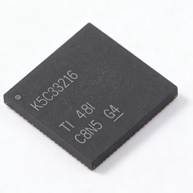
LMK5C33216RGCR - Ultra-Low Jitter Clock Synchronizer | TI
The Texas Instruments LMK5C33216RGCR is an ultra-low jitter clock synchronizer, jitter attenuator, and clock generator designed for wireless communications infrastructure. It integrates three high-performance digital phase-locked loops (DPLLs) with paired analog phase-locked loops (APLLs) and a BAW (Bulk Acoustic Wave) APLL that achieves 40 fs RMS jitter at 491.52 MHz. The device supports output frequencies up to 3 GHz and operates from a 3.3V supply in a 64-pin VQFN (RGC) package with exposed thermal pad. A clock synchronizer is a specialized timing IC that generates and aligns multiple clock signals to a reference, often cleaning jitter from noisy sources. In the hierarchy of timing components, a clock synchronizer sits above a simple PLL or clock generator, providing advanced features like hitless switching, holdover, and digital loop filtering. The LMK5C33216 is part of TI's LMK5C family, which targets 5G base stations, small cells, and other high-speed networking equipment where precise timing is critical for JESD204B data converters. Key features include three DPLLs with programmable loop bandwidth from 0.01 Hz to 4 kHz, eliminating the need for external loop filters. The BAW APLL delivers exceptional jitter performance of 40 fs RMS, while the device also offers -116 dBc/Hz phase noise at 100 Hz offset. It supports JESD204B interface for direct connection to high-speed ADCs and DACs, and includes advanced reference clock selection with hitless switching to maintain synchronization during reference failures. The LMK5C33216 integrates a flexible clock output architecture with multiple dividers and delays, allowing generation of various frequencies from a single reference. Its digital PLL architecture provides precise frequency synthesis and alignment, while the analog PLLs ensure low-noise output. The device is programmable via SPI or I2C, enabling dynamic reconfiguration in the field. Typical applications include 5G NR base stations, remote radio heads, small cells, and test and measurement equipment. The device is also suitable for optical transport networks and data center switches requiring high-frequency, low-jitter clocks. Its wide output frequency range and low jitter make it ideal for JESD204B converter clocking. When designing with the LMK5C33216, ensure proper power supply decoupling with low-ESR capacitors close to the VQFN pins. The exposed thermal pad must be soldered to a ground plane for adequate heat dissipation. Use the device's internal loop filters to simplify design, but verify loop bandwidth settings for your specific jitter transfer requirements.

MIC1557YM5TR - IttyBitty 555 RC Oscillator 5MHz SOT-23-5 | Microchip
The Microchip Technology MIC1557YM5TR is an IttyBitty CMOS RC oscillator in a 5-pin SOT-23-5 package, delivering rail-to-rail pulses for precise frequency generation up to 5 MHz from a 2.7V to 18V supply. It is a 555-type timing IC optimized as an oscillator-only device with shutdown control. A 555-type timer/oscillator is a classic analog building block that generates precise time delays or square-wave frequencies using an external resistor-capacitor (RC) network. Within the power-management and clock-timing hierarchy, it functions as a low-cost oscillator IC, sitting between discrete RC astable circuits and integrated clock generators. Key features include a wide 2.7V to 18V operating supply range, a 5 MHz maximum oscillation frequency, CMOS technology for low power consumption, and a shutdown pin that reduces quiescent draw to microamp levels. Rail-to-rail output pulses swing the full supply range, making the output directly compatible with both 3.3V and 5V logic when operated from those rails. The MIC1557 differs from its companion MIC1555 by internally tying the trigger and threshold comparators together, simplifying astable oscillator connections; the MIC1555 retains separate trigger and threshold pins for timer (one-shot) applications. Both devices replace the industry-standard NE555 in space-constrained designs where the 8-pin package is too large. Typical applications include LED flashers and lamp drivers, clock generation for microcontrollers and ADCs, pulse-width and frequency generation, precision time-delay generation, and watchdog or supervisory timing in battery-powered systems. Design tip: the oscillation frequency is set by one resistor from OUT to the threshold pin and one timing capacitor to ground; keep the timing capacitor dielectric stable (NPO/C0G ceramic) for frequency accuracy. This page synthesizes verified distributor pricing, drop-in alternative options, and practical design notes not found in the manufacturer datasheet.

NE555DR - Precision Timer IC 100kHz SOIC-8 | Texas Instruments
The Texas Instruments NE555DR is a precision timer IC in an 8-pin SOIC surface-mount package, capable of producing accurate time delays and oscillations from microseconds to hours. It operates from a 4.5V to 16V supply and supports both astable and monostable modes with adjustable duty cycle. A 555 timer is a classic analog timer and oscillator IC first introduced in the 1970s. Within the semiconductor hierarchy, it belongs to the clock and timing family: timer IC -> oscillator IC -> analog mixed-signal IC. The 555 architecture uses two comparators, a resistive voltage divider, and a discharge transistor to switch an external RC network, producing precise timing intervals defined by resistor and capacitor values. Key features include timing from microseconds to hours, astable or monostable operation, adjustable duty cycle, and a TTL-compatible output that can sink or source up to 200 mA - enough to drive LEDs, relays, or small motors directly without a buffer transistor. According to TI, on products compliant to MIL-PRF-38535, all parameters are tested unless otherwise noted. The bipolar process of the NE555 delivers robust drive capability and noise immunity, making it more forgiving in harsh environments than CMOS variants, at the cost of higher supply current (typ. [DATA_NEEDED: quiescent current]) and slightly less timing accuracy at temperature extremes. The 100 kHz maximum oscillation frequency covers most low-speed timing, pulse generation, and PWM tasks. Typical applications include LED flashers and lamp dimmers, pulse width modulation, tone and alarm generation, time-delay generation in industrial control, and clock generation for digital circuits. The SOIC-8 package suits automated assembly on modern PCBs. Design tip: keep the timing capacitor above 500 pF and use 1% resistors for best timing accuracy; add a 0.1 uF decoupling capacitor close to VCC to prevent supply glitches during output switching.
PCA8525 - Automotive TCXO-Style RTC IC 125C | NXP Semiconductors
The NXP Semiconductors PCA8525 is a high-accuracy, nano-powered Real Time Clock (RTC) IC with an integrated temperature compensation engine and an I2C serial interface, supplied in an automotive-qualified HVSON10 package and rated for ambient temperatures up to 125 degrees C. A Real Time Clock (RTC) is a timing integrated circuit that keeps track of seconds, minutes, hours, days, months, and years using an external 32.768 kHz watch crystal. Within the power-management and timing hierarchy, an RTC sits below the system microcontroller and above the raw crystal oscillator stage, providing calendar and timekeeping registers that survive main-power loss via a backup supply. Standard RTC ICs rely on an uncompensated crystal, whose frequency drifts with temperature. The PCA8525 is the first and only crystal-based RTC IC to feature a default temperature compensation engine. It compensates a typical crystal model selectable between -0.035 ppm/degC2 and -0.04 ppm/degC2, and combined with its aging offset feature it can achieve up to 5x better timekeeping accuracy than a standard RTC IC with an uncompensated crystal. Technically, the PCA8525 is a CMOS device optimized for nano-power consumption, with all addresses and data transferred serially over the I2C bus. The integrated temperature compensation engine measures the die temperature and applies digital frequency correction to the 32.768 kHz crystal, delivering module-class accuracy in a single IC without an external TCXO module. Typical applications include automotive body control modules, gateway and telematics units, industrial data loggers, and smart meters - anywhere accurate time stamps are required across a wide automotive temperature range. Design consideration: the temperature compensation engine assumes a typical tuning-fork crystal model; verify the selected crystal's parabolic coefficient matches the selectable -0.035 or -0.04 ppm/degC2 setting, and apply the aging offset register to trim long-term drift. This page synthesizes distributor pricing, drop-in alternatives, and practical design notes not found in the manufacturer datasheet.

PCF85063AT/AY - RTC, I2C 400kHz, SOIC-8 | NXP Semiconductors
The NXP Semiconductors PCF85063AT/AY is a tiny CMOS Real-Time Clock (RTC) and calendar IC with alarm function and a 400 kbit/s I2C-bus interface, housed in an 8-pin SOIC (SO8, 0.154 inch / 3.90 mm width) package. A Real-Time Clock (RTC) is a timekeeping IC that tracks seconds, minutes, hours, days, weekdays, months, and years while the main processor sleeps or is powered down. Within the power-management and clock/timing IC hierarchy, an RTC sits alongside microcontroller supervisory functions and is typically paired with a 32.768 kHz crystal and a backup coin cell so that time-of-day data survives main-power loss. Key features of the PCF85063AT/AY include year 2000-compliant calendar with automatic leap-year correction, an alarm function with interrupt output, an offset register that allows fine-tuning of the clock for crystal-frequency correction, and a 32.768 kHz reference optimized for low power consumption. The device communicates over a two-line bidirectional I2C-bus with a maximum data rate of 400 kbit/s, and the register address increments automatically after each written or read data byte. The CMOS architecture keeps standby current extremely low, which directly extends backup-battery life in metering and battery-powered designs. The offset register enables software calibration, compensating for crystal tolerance without an external trimming capacitor - a meaningful advantage for high-volume production where per-unit crystal spread would otherwise require manual adjustment. Typical applications include smart meters and utility metering, battery-powered portable and wearable devices, industrial controllers that must retain time across power cycles, and automotive-adjacent systems via the AEC-Q100-qualified PCF85063AT/AAZ variant. When designing with this device, place the 32.768 kHz crystal as close as possible to the OSCI/OSCO pins, use a guaranteed 32.768 kHz crystal with the load capacitance specified in the NXP datasheet, and route the I2C SDA/SCL lines away from noisy switching nodes. This page synthesizes distributor pricing, drop-in alternatives, pinout, and practical design notes not found in the manufacturer datasheet.
PCF8525 - ±30ppm Temperature-Compensated RTC | NXP
The NXP PCF8525 is a high-accuracy, nano-powered real-time clock (RTC) IC with an I2C interface, offering up to ±30 ppm timekeeping accuracy in the temperature-compensated HVSON10 package variant, and an ultra-compact WLCSP variant (PCF8525TKX) for space-constrained designs. A real-time clock IC is a dedicated timekeeping device that maintains seconds, minutes, hours, day, weekday, month, and year counters while the host system sleeps or is powered down. Within the system hierarchy, an RTC sits below the power management IC and alongside supervisory circuits, feeding timestamp data to a microcontroller over a serial bus such as I2C. External RTCs like the PCF8525 offload timekeeping from the main SoC, cutting system power demands significantly - NXP states its RTC/calendar family can cut power demands by as much as 60 percent. The defining feature of the PCF8525 is that it is the first and only external-crystal RTC IC to feature a default temperature compensation engine. It compensates for a typical crystal model, selectable between -0.035 ppm/degC2 and -0.04 ppm/degC2 parabolic coefficients, and adds an aging offset register for long-term drift correction. According to NXP, this yields up to 5x better timekeeping accuracy than a standard uncompensated RTC plus crystal. Architecturally, the device uses a CMOS timekeeping core clocked from an external 32.768 kHz crystal, with the compensation engine digitally correcting frequency versus temperature. The HVSON10 version includes full temperature compensation (±30 ppm class accuracy), while the WLCSP variant omits compensation in exchange for an ultra-compact footprint. Typical applications include battery-powered IoT sensor nodes, smart meters, data loggers, and industrial controllers requiring accurate timestamping with minimal standby current. Design consideration: select a 32.768 kHz crystal whose parabolic coefficient matches the selectable compensation model, and verify the I2C bus pull-up values for the target data rate. This page synthesizes verified distributor listings, drop-in alternative analysis, and practical design notes not found in the manufacturer datasheet alone.
PCF8583T/5 - I2C RTC Calendar with 256x8 RAM | NXP
The NXP PCF8583T/5 is a real-time clock/calendar IC with a 2048-bit static CMOS RAM organized as 256 words by 8 bits, a two-line bidirectional I2C-bus interface, and an SO-8 (SOIC-8) surface-mount package. It operates from a 32.768 kHz crystal, tracks clock, calendar, weekday, and counter modes, and provides 240 bytes of free user RAM. A real-time clock (RTC) is a timekeeping IC that maintains seconds, minutes, hours, date, month, year, and weekday information using a low-frequency crystal oscillator. RTCs form part of the broader timing IC family alongside clock buffers and supervisors, and are foundational power-management companions in any battery-backed embedded system that must keep time when main power is absent. Key features include the 256 x 8-bit low-power static CMOS RAM, automatic word address incrementing after each read or written data byte, an A0 address pin allowing two devices on one I2C bus, programmable alarm and timer functions, and an interrupt output (INT) that can assert on alarm or timer events. Architecturally, the PCF8583 divides the 32.768 kHz oscillator output down to 1 Hz for the time-counting chain and stores all counters and control registers within the on-chip RAM map, giving software a flat, I2C-addressable register file. CMOS design keeps supply current in the microampere class, enabling years of operation from a lithium coin cell. Typical applications include utility meters, battery-powered data loggers, set-top boxes, white goods, and industrial control panels requiring time-stamping and calendar-driven events. A critical design consideration is the 32.768 kHz crystal layout: keep oscillator traces short and guard them from noisy digital lines, since PCB contamination or stray coupling can cause timekeeping drift or startup failure. This page synthesizes distributor availability, drop-in alternative guidance, and practical design notes not found in the manufacturer datasheet, helping engineers source and apply the PCF8583T/5 with confidence.

SI5365-C-GQ - 1.05GHz Pin-Programmable Clock Multiplier | Skyworks
The Skyworks Solutions SI5365-C-GQ is a pin-programmable precision clock multiplier and jitter attenuator built on third-generation DSPLL technology, synthesizing any output frequency from 100 kHz to 1.05 GHz in a 100-pin TQFP (GQ) package. It integrates a low-noise VCO and eliminates the need for an external VCXO and loop filter components. A clock multiplier (also called a jitter-attenuating clock generator) is a timing IC in the broader clock generation and frequency synthesis hierarchy that takes a reference input and produces a clean, multiplied output clock. Jitter attenuators sit between a noisy reference source and a jitter-sensitive receiver, using a narrow-bandwidth phase-locked loop to remove accumulated jitter. The Si5365 belongs to the class of PLL-based clock multiplier ICs used in synchronous networking and high-speed serial systems. Key features include any-frequency synthesis from 100 kHz to 1.05 GHz, a digitally programmable PLL loop bandwidth selectable from 150 kHz to 1.3 MHz via the BWSEL[1:0] pins, and pin-programmable frequency configuration that requires no host processor or EEPROM programming. The DSPLL architecture suppresses reference spurs and delivers low phase noise suitable for SONET/SDH-class jitter masks. Technically, the device operates as a digital PLL with a high-resolution delta-sigma fractional-N feedback path, so output-to-input ratios can be any rational number within the operating ranges. Because the loop bandwidth is digitally set rather than set by RC components, jitter performance is repeatable from unit to unit and across temperature. Typical applications include line-card and optical module clock distribution, SONET/SDH and OTN equipment timing, 10G Ethernet and Fibre Channel transceiver reference clocks, and jitter cleanup for recovered clocks from retiming circuits. Design consideration: choose the BWSEL setting to balance jitter attenuation bandwidth against input tracking; a narrower bandwidth gives lower integrated jitter but less tolerance to reference wander. This page synthesizes distributor pricing, drop-in alternative data, and practical design notes not found in the manufacturer datasheet.
SI5365-C-GQR - 1.05GHz Any-Frequency Clock Multiplier | Skyworks
The Skyworks Solutions SI5365-C-GQR is a low-jitter any-frequency precision clock multiplier IC with a maximum output frequency of 1.05 GHz, four clock inputs from 19.44 MHz to 707.35 MHz, and five frequency-multiplied outputs, housed in a 100-pin TQFP package supplied on tape and reel. Based on Skyworks third-generation DSPLL technology, it integrates the complete PLL function including an internal VCXO and loop filter, eliminating external loop components and simplifying frequency synthesis designs. A clock multiplier (frequency synthesizer) is a timing IC that generates output clocks at an integer or fractional multiple of a reference input frequency. Within the timing hierarchy it sits under clock generators and PLL (phase-locked loop) devices, serving as the precision timing backbone for serial links, line cards, and backplane systems where stable, low-jitter reference clocks are critical to bit-error-rate performance. Key features include selectable output frequencies up to 1050 MHz, digitally programmable PLL loop bandwidth from 150 kHz to 1.3 MHz via BWSEL[1:0] pins, and flexible output signaling on CML, LVDS, LVPECL, and LVCMOS levels. The four-input, five-output architecture supports redundant reference clocking and fan-out of multiplied clocks to multiple serializers or PHYs. Technically, the DSPLL architecture replaces the analog loop filter and external VCXO of a classical PLL with a digital loop, giving deterministic bandwidth control and jitter attenuation that does not degrade across process, voltage, and temperature. This makes it well suited to SONET OC-48/OC-192, 10 Gigabit Ethernet, and Fibre Channel timing requirements. Typical applications include optical transport network line cards, Ethernet switch and router clock trees, and Fibre Channel storage network timing, where any-frequency synthesis from 19.44 MHz or 156.25 MHz references is required. Design consideration: note that the SI5365 is a clock multiplier without jitter attenuation of upstream references; the Si5366 family should be evaluated when reference jitter cleanup is required. Also, this device is marked not recommended for new designs. This page synthesizes distributor pricing, drop-in alternatives, and practical design notes not found in the manufacturer datasheet.
SI5366-B-GQ - Precision Clock Multiplier/Jitter Attenuator | Silicon Labs
The Silicon Labs SI5366-B-GQ is a jitter-attenuating precision clock multiplier that accepts four clock inputs from 8 kHz to 707 MHz and generates five frequency-multiplied clock outputs from 8 kHz to 1050 MHz, housed in a 100-pin TQFP package. Based on the Silicon Labs DSPLL architecture, it targets high-speed communication systems including SONET OC-48/OC-192, Ethernet, and Fibre Channel. A precision clock multiplier/jitter attenuator is a phase-locked-loop (PLL) based timing device that cleans a noisy reference clock and synthesizes a higher-frequency, low-jitter output locked to that reference. In the system hierarchy it sits within the clock generation and distribution layer of the timing chain: oscillator (reference) -> clock multiplier/jitter attenuator -> clock distribution -> SERDES/FPGA/ASIC clocks. Jitter attenuation is essential because the PLL bandpass filters the reference clock, suppressing reference spurs and wander while delivering a stable output at the line rate. Key features of the SI5366 include four selectable clock inputs spanning 8 kHz to 707 MHz, five frequency-multiplied outputs spanning 8 kHz to 1050 MHz, DSPLL-based jitter cleaning for SONET-grade compliance, and pin-programmable configuration (the B-grade part is set via pin straps rather than in-circuit register programming), simplifying designs that avoid a microcontroller on the timing board. The device operates from a nominal 3.3 V supply per Silicon Labs documentation and is specified for communication-grade temperature ranges. Technically, the Si5366 uses Silicon Labs' digital DSPLL loop architecture, in which the loop bandwidth is set digitally, providing deterministic jitter transfer and enabling tight reference-to-output frequency mapping suitable for OC-48 (622.08 MHz) and OC-192 (9953.28 MHz SERDES reference) line cards. It replaces discrete VCXO-plus-PLL loops with a single-chip solution and supports hitless reference switching between redundant inputs. Typical applications include SONET/SDH OTN line cards, 10 GbE and Fibre Channel (1x/2x/4x/10x) transceiver reference clocks, Synchronous Ethernet timing cards, and test equipment clock synthesis. The five outputs allow one device to clock a SERDES, FPGA, PHY, and ASIC simultaneously. Design consideration: verify the selected loop bandwidth against the applicable jitter transfer mask for your standard, and decouple all supply pins with low-ESR ceramics placed directly at the TQFP power pins. This page synthesizes distributor availability, drop-in alternatives, and practical design notes not found in the manufacturer datasheet.
SI5366-C-GQ - 1.05GHz Jitter Attenuator Clock Multiplier | Skyworks
The Skyworks Solutions SI5366-C-GQ is a jitter-attenuating precision clock multiplier IC that accepts four clock inputs from 8 kHz to 707 MHz and generates five frequency-multiplied clock outputs from 8 kHz to 1050 MHz, with jitter generation as low as 0.3 ps rms (12 kHz to 20 MHz), housed in a 100-pin TQFP package. A jitter attenuator is a specialized clock generator built around a phase-locked loop (PLL) that cleans reference clocks by narrowing their jitter distribution while synthesizing output frequencies. Within the timing hierarchy, the Si5366 belongs to the clock multiplier and frequency synthesizer family, positioned below full network synchronization cards but above simple zero-delay buffers, and it serves as the timing backbone for synchronous optical networking (SONET), Ethernet, and Fibre Channel line cards. Key features include selectable output frequencies from 8 kHz to 1050 MHz, third-generation DSPLL technology, an integrated loop filter with selectable loop bandwidth from 60 Hz to 8.4 kHz, four clock inputs with manual or automatic hitless switching, and output logic levels selectable among CML, CMOS, LVDS, and LVPECL. The C-grade option delivers 0.3 ps rms typical jitter generation and meets OC-192 GR-253-CORE jitter specifications, making it suitable for the most demanding telecom compliance regimes. Technically, the DSPLL architecture replaces conventional discrete RC loop filters with an on-chip digital loop filter, enabling precise bandwidth programmability without external components and superior tolerance of noisy references. Frequency plans are configured through in-circuit programming rather than factory pin-strapping, allowing one device to serve many clocking architectures. Typical applications include SONET OC-48/OC-192 line-card clock recovery and synthesis, 10 Gigabit Ethernet PHY reference clocking, Fibre Channel storage-area-network switching, and telecom transport equipment requiring hitless reference switching between redundant sources. A key design consideration is power supply integrity: high-speed CML and LVPECL outputs demand clean 2.5V/3.3V rails and solid ground planes; omitting proper decoupling at the PLL supply pins degrades the sub-picosecond jitter floor. This page synthesizes distributor pricing, drop-in alternatives, design notes, and compliance data not found in the manufacturer datasheet alone.
SI5366-C-GQR - 1.05GHz Jitter Attenuator Clock IC | Skyworks
The Skyworks Solutions (Silicon Labs) SI5366-C-GQR is a jitter-attenuating precision clock multiplier that accepts four clock inputs from 8 kHz to 707 MHz and generates five frequency-multiplied outputs from 8 kHz to 1050 MHz, housed in a 100-pin TQFP (14x14 mm) package. A jitter attenuator, also called a jitter cleaner or synchronizing clock multiplier, is a clock-timing IC built around a phase-locked loop (PLL) that takes a noisy or frequency-multiplexed reference clock and produces a low-jitter output locked to that reference. Within the clock management hierarchy, it sits between oscillators/clock generators and the high-speed serializers, FPGAs, and ASICs that consume the resulting clocks, making it a core building block of communication-system clock trees. Key features include third-generation DSPLL technology for any-frequency clock synthesis, four selectable input references covering 8 kHz to 707.35 MHz, five independent outputs reaching 1049.76 MHz, and flexible output signaling with CML, CMOS, LVDS, and LVPECL levels. This combination lets one device serve both slow SONET synchronization references (such as 19.44 MHz or 8 kHz) and fast 622 MHz or 1 GHz serial-link clocks. Architecturally, the digital PLL (DSPLL) replaces traditional analog loop-filter components with an on-chip digital loop filter, eliminating external RC tuning, improving repeatability, and enabling loop bandwidth selection without hardware changes. The C-grade device targets commercial operating ranges typical of communications equipment. Typical applications include SONET OC-48/OC-192 line cards, Ethernet and Fibre Channel switch and router timing, and wireless baseband clock distribution where a jitter-cleaned reference drives data converters or SERDES blocks. Design consideration: match the DSPLL loop bandwidth to the jitter transfer mask of your standard (e.g., SONET/SDH) and keep the 100-pin TQFP power pins well decoupled to preserve phase-noise performance. This page synthesizes distributor pricing, drop-in family alternatives, and practical design notes not found in the manufacturer datasheet.